Nanomaterials for Plasmonic Devices. Lih J. Chen
|
|
|
- Heather Merritt
- 5 years ago
- Views:
Transcription
1 Nanomaterials for Plasmonic Devices Lih J. Chen Department of Materials Science and Engineering, National Tsing Hua University, Hsinchu, Taiwan
")
2 Papers on Plasmon: 75,000 (6/25/2018)

3 Papers on Plasmonics: 31,262 (6/22/2018)

4 M.L. Juan et al. Nature Photonics 5, 349 (2011)
5
")
6 Papers on Plasmon: 75,000 (6/25/2018)
7 O1. Plasmonic laser (optical circuit) O2. Nanoantennas O3. Photodetectors E1. H 2 production (energy/environment) E2. Dye-sensitized solar cells E3. Photocatalytic activities S1. Detectors for intermediates (sensing)
8
9
10

11 All-Color Plasmonic Nanolasers Y.J. Lu et al. Nano Lett. 14, 4381 (2014)

 C.")
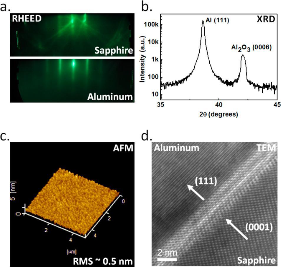
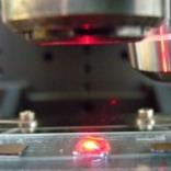
12 Room temperature UV nanolaser (a) Real and (b) imaginary parts of the permittivities of Al, Au and Ag. Davy, G. et al. Journal of Physics D: Applied Physics. 48 (2015) C.W. Cheng et al. ACS Photonics (2018)


13 Properties of ZnO 1. II-VI semiconductor group 2. Melting point: Crystal structure: Wurtzite structure/ Zinc blende structure 4. Wide and direct band gap : 3.37eV 5. Large exciton binding energy: 60meV
14 Intensity (arb. units) FWHM (nm) Intensity (arb. units) Plasmonic lasers MW/cm MW/cm MW/cm MW/cm 2 Pump density (MW/cm 2 ) Wavelength (nm) 14

15
16
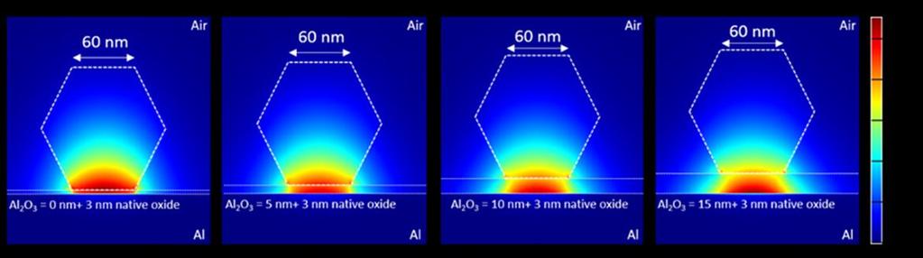
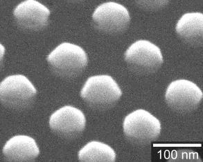
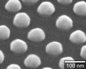
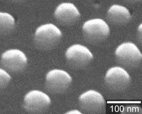
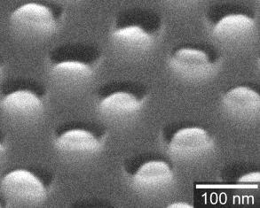
17 Group index Threshold power (MW/cm 2 ) Effect of Al 2 O 3 thickness on optical properties n g =(λ 2 /2 Δ λl) nm 5 nm 10 nm 15 nm Thickness of Al 2 O 3 0 nm 5 nm 10 nm 15 nm Thickness of Al 2 O 3 17


18 Field energy density Simulation Al 2 O 3 = 360 nm Al 2 O 3 = 5 nm Al 2 O 3 = 10 nm Al 2 O 3 = 15 nm max Wavelength= nm min

19 19

20 EDS ALD Al 2 O 3 Eleme nt Weight % Atomic % O K Al K Native Al 2 O 3 Eleme nt Weight % Atomic % O K Al K


21 AFM Native Al 2 O 3 r ms = 1.14 nm ALD-grown Al 2 O 3 r ms = 0.87 nm


22 The order in energy density for the 3 dielectric layers : Y 2 O 3 > TiO 2 >Al 2 O 3 with stimulated wavelength of 378 nm.
23 Au Nanocrystal Array/Silicon Nanoantennas as Wavelength- Selective Photoswitches Y.K. Lin et al. Nano Lett. 13, 2723 (2013)

24 Experimental Metal-assisted Chemical Etching (MaCE) H 2 O H2 O 2 Cathode reaction H 2 O 2 + 2H + 2H 2 O + 2h + HF Anode reaction Si + 4HF 2 SiF HF + H 2 +2e Nano Structures and Dynamics Lab 24
25 Results Au-Nanocrystal-Array/Si Nanostructures with Varied Degree of Immersion DOI: Degree of Immersion DOI = 0 DOI = 0.25 DOI = 0.5 DOI = 0.75 DOI = 1 Nano Structures and Dynamics Lab 25


 = I light - I dark 0 k E z")
26 I light - I dark ( A / W) Results Photocurrent Increment under 532 nm Laser Illumination 5 4 DOI = 0 DOI = 0.5 bare Si log 10 E 2 2 z λ = 532 nm 3 2 z Si bare Si 1 Au/Ti Au/Ti Si Voltage (mv) I light : current measured under laser illumination I dark : current measured under dark condition DI (Photocurrent increment) = I light - I dark 0 k E z Si DOI = 0 Si DOI = 0.5 Nano Structures and Dynamics Lab 26


27 I light - I dark ( A / W) Results Photocurrent Increment under 655 nm Laser Illumination 1.5 DOI = 0 DOI = 0.5 bare Si log 10 E 2 2 z λ = 655 nm Si 1.0 z bare Si 0.5 Au/Ti Au/Ti Si Voltage (mv) I light : current measured under laser illumination I dark : current measured under dark condition DI (Photocurrent increment) = I light - I dark 0 k E z Si DOI = 0 Si DOI = 0.5 Nano Structures and Dynamics Lab 27
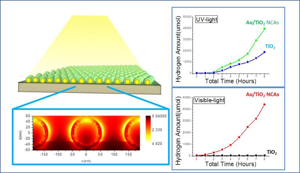
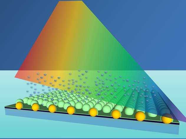
28 Plasmon-Enhanced Photocatalytic Hydrogen Production on Au/TiO 2 Hybrid Nanocrystal Arrays B.H. Wu et al. Nano Energy, 27, (2016)
29
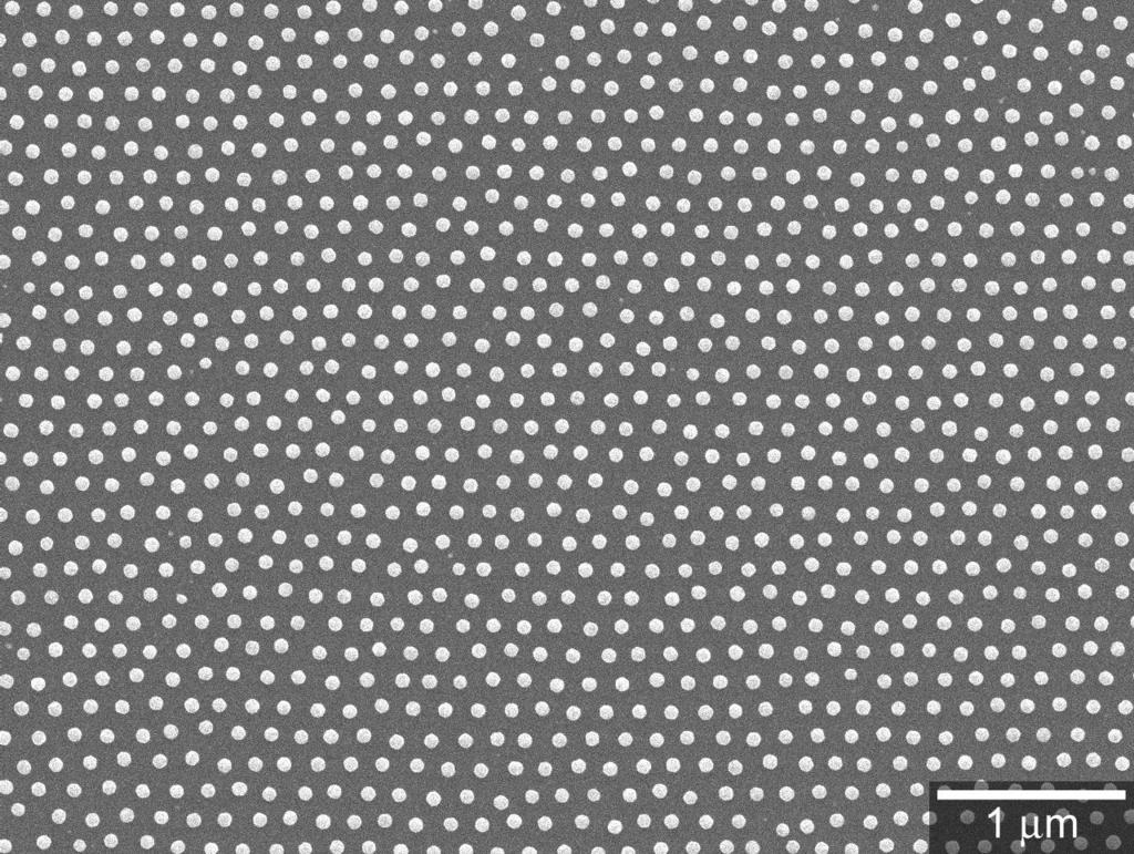
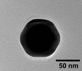
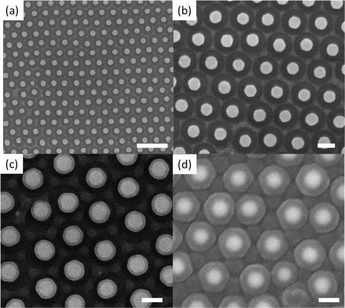
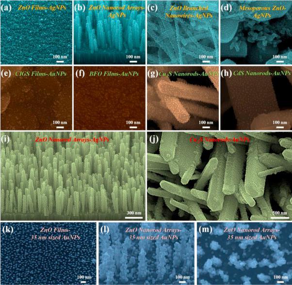
30
31 Surface Plasmon Resonance Enhancement of Production of H 2 from Ammonia Borane Solution with Tunable Cu 2-x S Nanowires Decorated by Pd Nanoparticles P.H. Liu et al. Nano Energy, 31, (2017).

32 Pei-Hsuan Liu, Meicheng Wen, Chih-Shan Tan, Miriam Navlani-García, Yasutaka Kuwahara, Kohsuke Mori, Hiromi Yamashita, Lih-Juann Chen Surface plasmon resonance enhancement of production of H2 from ammonia borane solution with tunable Cu2 xs nanowires decorated by Pd nanoparticles Nano Energy, Volume 31, 2017,
33 Plasmonic Enhancement of Au Nanoparticle Embedded Single- Crystalline ZnO Nanowire Dye- Sensitized Solar Cells M.Y. Lu et al. Nano Energy 20, (2016)
34
35
36 Ultrahigh density plasmonic hot spots with ultrahigh electromagnetic field for improved photocatalytic activities T.H. Yang et al. Applied Catalysis B: Environmental 181, (2016)
37

38
39 O1. Plasmonic laser (optical circuit) O2. Nanoantennas O3. Photodetectors E1. H 2 production (energy/environment) E2. Dye-sensitized solar cells E3. Photocatalytic activities S1. Detectors for intermediates (sensing)
40


41 a b 1 μm 200 nm c d

42 C.S. Tan et al. Scientific Reports, 5, (2015)
43 O1. Plasmonic laser (optical circuit) O2. Nanoantennas O3. Photodetectors E1. H 2 production (energy/environment) E2. Dye-sensitized solar cells E3. Photocatalytic activities S1. Detectors for intermediates (sensing)
")
44 Papers on Plasmon: 75,000 (6/25/2018)


45 Thanks for Your Attention
III-V nanostructured materials synthesized by MBE droplet epitaxy
 III-V nanostructured materials synthesized by MBE droplet epitaxy E.A. Anyebe 1, C. C. Yu 1, Q. Zhuang 1,*, B. Robinson 1, O Kolosov 1, V. Fal ko 1, R. Young 1, M Hayne 1, A. Sanchez 2, D. Hynes 2, and
Nano Optics Based on Coupled Metal Nanoparticles
 Nano Optics Based on Coupled Metal Nanoparticles Shangjr Gwo ( 果尚志 ) Department of Physics National Tsing-Hua University, Hsinchu 30013, Taiwan E-mail: gwo@phys.nthu.edu.tw NDHU-Phys (2010/03/01) Background
REFRACTORY METAL OXIDES: FABRICATION OF NANOSTRUCTURES, PROPERTIES AND APPLICATIONS
 REFRACTORY METAL OXIDES: FABRICATION OF NANOSTRUCTURES, PROPERTIES AND APPLICATIONS S.K. Lazarouk, D.A. Sasinovich BELARUSIAN STATE UNIVERSITY OF INFORMATICS AND RADIOELECTRONICS Outline: -- experimental
Supplementary Information
 Electronic Supplementary Material (ESI) for Journal of Materials Chemistry A. This journal is The Royal Society of Chemistry 2015 Supplementary Information Engineering the Intermediate Band States in Amorphous
Photovoltaic Enhancement Due to Surface-Plasmon Assisted Visible-Light. Absorption at the Inartificial Surface of Lead Zirconate-Titanate Film
 Photovoltaic Enhancement Due to Surface-Plasmon Assisted Visible-Light Absorption at the Inartificial Surface of Lead Zirconate-Titanate Film Fengang Zheng, a,b, * Peng Zhang, a Xiaofeng Wang, a Wen Huang,
Supporting Information. InGaAs Nanomembrane/Si van der Waals Heterojunction. Photodiodes with Broadband and High Photoresponsivity
 Supporting Information InGaAs Nanomembrane/Si van der Waals Heterojunction Photodiodes with Broadband and High Photoresponsivity Doo-Seung Um, Youngsu Lee, Seongdong Lim, Jonghwa Park, Wen-Chun Yen, Yu-Lun
Gas Sensors and Solar Water Splitting. Yang Xu
 Gas Sensors and Solar Water Splitting Yang Xu 11/16/14 Seite 1 Gas Sensor 11/16/14 Seite 2 What are sensors? American National Standards Institute (ANSI) Definition: a device which provides a usable output
Optimizing the performance of metal-semiconductor-metal photodetectors by embedding nanoparticles in the absorption layer
 Journal of Electrical and Electronic Engineering 2015; 3(2-1): 78-82 Published online February 10, 2015 (http://www.sciencepublishinggroup.com/j/jeee) doi: 10.11648/j.jeee.s.2015030201.27 ISSN: 2329-1613
NSF EPSCoR Kansas Center for Solar Energy Research Annual Program Review June 12-14, 2011
 NSF EPSCoR Kansas Center for Solar Energy Research Annual Program Review June 12-14, 2011 Plasmonic and Photonic Photovoltaics based on graphene and other carbon nanostructures Fengli Wang, Guowei Xu,
Strong light matter coupling in two-dimensional atomic crystals
 SUPPLEMENTARY INFORMATION DOI: 10.1038/NPHOTON.2014.304 Strong light matter coupling in two-dimensional atomic crystals Xiaoze Liu 1, 2, Tal Galfsky 1, 2, Zheng Sun 1, 2, Fengnian Xia 3, Erh-chen Lin 4,
Nanoscale optical circuits: controlling light using localized surface plasmon resonances
 Nanoscale optical circuits: controlling light using localized surface plasmon resonances T. J. Davis, D. E. Gómez and K. C. Vernon CSIRO Materials Science and Engineering Localized surface plasmon (LSP)
Nanostructures. Lecture 13 OUTLINE
 Nanostructures MTX9100 Nanomaterials Lecture 13 OUTLINE -What is quantum confinement? - How can zero-dimensional materials be used? -What are one dimensional structures? -Why does graphene attract so much
Nanostrukturphysik (Nanostructure Physics)
") Nanostrukturphysik (Nanostructure Physics) Prof. Yong Lei & Dr. Yang Xu Fachgebiet 3D-Nanostrukturierung, Institut für Physik Contact: yong.lei@tu-ilmenau.de; yang.xu@tu-ilmenau.de Office: Unterpoerlitzer
Nanostrukturphysik (Nanostructure Physics) Prof. Yong Lei & Dr. Yang Xu Fachgebiet 3D-Nanostrukturierung, Institut für Physik Contact: yong.lei@tu-ilmenau.de; yang.xu@tu-ilmenau.de Office: Unterpoerlitzer
Nanocomposite photonic crystal devices
 Nanocomposite photonic crystal devices Xiaoyong Hu, Cuicui Lu, Yulan Fu, Yu Zhu, Yingbo Zhang, Hong Yang, Qihuang Gong Department of Physics, Peking University, Beijing, P. R. China Contents Motivation
Supplementary Figure 1
 Supplementary Figure 1 XRD patterns and TEM image of the SrNbO 3 film grown on LaAlO 3(001) substrate. The film was deposited under oxygen partial pressure of 5 10-6 Torr. (a) θ-2θ scan, where * indicates
Graphene photodetectors with ultra-broadband and high responsivity at room temperature
 SUPPLEMENTARY INFORMATION DOI: 10.1038/NNANO.2014.31 Graphene photodetectors with ultra-broadband and high responsivity at room temperature Chang-Hua Liu 1, You-Chia Chang 2, Ted Norris 1.2* and Zhaohui
Nanochannel-Assisted Perovskite Nanowires: Growth Mechanisms. to Photodetector Applications
 Supplementary Information: Nanochannel-Assisted Perovskite Nanowires: Growth Mechanisms to Photodetector Applications Qitao Zhou, Jun Gyu Park, Riming Nie, Ashish Kumar Thokchom, Dogyeong Ha, Jing Pan,
Abnormal PL spectrum in InGaN MQW surface emitting cavity
 Abnormal PL spectrum in InGaN MQW surface emitting cavity J. T. Chu a, Y.-J. Cheng b, H. C. Kuo a, T. C. Lu a, and S. C. Wang a a Department of Photonics & Institute of Electro-Optical Engineering, National
PLASMONICS/METAMATERIALS
 PLASMONICS/METAMATERIALS Interconnects Optical processing of data Subwavelength confinement Electrodes are in place Coupling to other on-chip devices Combination of guiding, detection, modulation, sensing
Progress Report to AOARD
 Progress Report to AOARD C. C. (Chih-Chung) Yang The Graduate Institute of Electro-Optical Engineering National Taiwan University No. 1, Roosevelt Road, Section 4, Taipei, Taiwan (phone) 886-2-23657624
3.1 Absorption and Transparency
 3.1 Absorption and Transparency 3.1.1 Optical Devices (definitions) 3.1.2 Photon and Semiconductor Interactions 3.1.3 Photon Intensity 3.1.4 Absorption 3.1 Absorption and Transparency Objective 1: Recall
All-Inorganic Perovskite Solar Cells
 Supporting Information for: All-Inorganic Perovskite Solar Cells Jia Liang, Caixing Wang, Yanrong Wang, Zhaoran Xu, Zhipeng Lu, Yue Ma, Hongfei Zhu, Yi Hu, Chengcan Xiao, Xu Yi, Guoyin Zhu, Hongling Lv,
Nanophysics: Main trends
 Nano-opto-electronics Nanophysics: Main trends Nanomechanics Main issues Light interaction with small structures Molecules Nanoparticles (semiconductor and metallic) Microparticles Photonic crystals Nanoplasmonics
Supplementary Information. Atomic Layer Deposition of Platinum Catalysts on Nanowire Surfaces for Photoelectrochemical Water Reduction
 Supplementary Information Atomic Layer Deposition of Platinum Catalysts on Nanowire Surfaces for Photoelectrochemical Water Reduction Neil P. Dasgupta 1 ǂ, Chong Liu 1,2 ǂ, Sean Andrews 1,2, Fritz B. Prinz
Supporting Information. 1T-Phase MoS 2 Nanosheets on TiO 2 Nanorod Arrays: 3D Photoanode with Extraordinary Catalytic Performance
 Supporting Information 1T-Phase MoS 2 Nanosheets on Nanorod Arrays: 3D Photoanode with Extraordinary Catalytic Performance Yuxi Pi, Zhen Li, Danyun Xu, Jiapeng Liu, Yang Li, Fengbao Zhang, Guoliang Zhang,
Large-Area and Uniform Surface-Enhanced Raman. Saturation
 Supporting Information Large-Area and Uniform Surface-Enhanced Raman Spectroscopy Substrate Optimized by Enhancement Saturation Daejong Yang 1, Hyunjun Cho 2, Sukmo Koo 1, Sagar R. Vaidyanathan 2, Kelly
Efficient Hydrogen Evolution. University of Central Florida, 4000 Central Florida Blvd. Orlando, Florida, 32816,
 Electronic Supplementary Material (ESI) for Energy & Environmental Science. This journal is The Royal Society of Chemistry 2017 MoS 2 /TiO 2 Heterostructures as Nonmetal Plasmonic Photocatalysts for Highly
Wednesday 3 September Session 3: Metamaterials Theory (16:15 16:45, Huxley LT308)
") Session 3: Metamaterials Theory (16:15 16:45, Huxley LT308) (invited) TBC Session 3: Metamaterials Theory (16:45 17:00, Huxley LT308) Light trapping states in media with longitudinal electric waves D McArthur,
Session 3: Metamaterials Theory (16:15 16:45, Huxley LT308) (invited) TBC Session 3: Metamaterials Theory (16:45 17:00, Huxley LT308) Light trapping states in media with longitudinal electric waves D McArthur,
ME 4875/MTE C16. Introduction to Nanomaterials and Nanotechnology. Lecture 2 - Applications of Nanomaterials + Projects
 ME 4875/MTE 575 - C16 Introduction to Nanomaterials and Nanotechnology Lecture 2 - Applications of Nanomaterials + Projects 1 Project Teams of 4 students each Literature review of one application of nanotechnology
Optical Characteristics of ZnO Based Photodetectors Doped with Au Nanoparticles
 nd International Conference on Mechanical and Electronics Engineering (ICMEE ) Optical Characteristics of ZnO Based Photodetectors Doped with Au Nanoparticles S. Mohammadnejad, S. G. Samani, and E. Rahimi
Plasmonic Hot Hole Generation by Interband Transition in Gold-Polyaniline
 Supplementary Information Plasmonic Hot Hole Generation by Interband Transition in Gold-Polyaniline Tapan Barman, Amreen A. Hussain, Bikash Sharma, Arup R. Pal* Plasma Nanotech Lab, Physical Sciences Division,
A Study on the Suitability of Indium Nitride for Terahertz Plasmonics
 A Study on the Suitability of Indium Nitride for Terahertz Plasmonics Arjun Shetty 1*, K. J. Vinoy 1, S. B. Krupanidhi 2 1 Electrical Communication Engineering, Indian Institute of Science, Bangalore,
The interfacial study on the Cu 2 O/Ga 2 O 3 /AZO/TiO 2 photocathode for water splitting fabricated by pulsed laser deposition
 Electronic Supplementary Material (ESI) for Catalysis Science & Technology. This journal is The Royal Society of Chemistry 2017 The interfacial study on the Cu 2 O/Ga 2 O 3 /AZO/TiO 2 photocathode for
Supplementary material for High responsivity mid-infrared graphene detectors with antenna-enhanced photo-carrier generation and collection
 Supplementary material for High responsivity mid-infrared graphene detectors with antenna-enhanced photo-carrier generation and collection Yu Yao 1, Raji Shankar 1, Patrick Rauter 1, Yi Song 2, Jing Kong
Supplementary information
 Supplementary information Improving the Working Efficiency of a Triboelectric Nanogenerator by the Semimetallic PEDOT:PSS Hole Transport Layer and its Application in Self- Powered Active Acetylene Gas
GRAPHENE EFFECT ON EFFICIENCY OF TiO 2 -BASED DYE SENSITIZED SOLAR CELLS (DSSC)
") Communications in Physics, Vol. 26, No. 1 (2016), pp. 43-49 DOI:10.15625/0868-3166/26/1/7961 GRAPHENE EFFECT ON EFFICIENCY OF TiO 2 -BASED DYE SENSITIZED SOLAR CELLS (DSSC) NGUYEN THAI HA, PHAM DUY LONG,
Communications in Physics, Vol. 26, No. 1 (2016), pp. 43-49 DOI:10.15625/0868-3166/26/1/7961 GRAPHENE EFFECT ON EFFICIENCY OF TiO 2 -BASED DYE SENSITIZED SOLAR CELLS (DSSC) NGUYEN THAI HA, PHAM DUY LONG,
ABSTRACT 1. INTRODUCTION 2. EXPERIMENT
 Fabrication of Nanostructured Heterojunction LEDs Using Self-Forming Moth-Eye Type Arrays of n-zno Nanocones Grown on p-si (111) Substrates by Pulsed Laser Deposition D. J. Rogers 1, V. E. Sandana 1,2,3,
Special Topics in Semiconductor Nanotechnology ECE 598XL
 Special Topics in Semiconductor Nanotechnology ECE 598XL Fall 2009 ECE 598XL Syllabus Overview: size matters Formation Process Characterization SOA device applications and potentials Homework or quizzes
vapour deposition. Raman peaks of the monolayer sample grown by chemical vapour
 Supplementary Figure 1 Raman spectrum of monolayer MoS 2 grown by chemical vapour deposition. Raman peaks of the monolayer sample grown by chemical vapour deposition (S-CVD) are peak which is at 385 cm
Electroluminescence from Silicon and Germanium Nanostructures
 Electroluminescence from silicon Silicon Getnet M. and Ghoshal S.K 35 ORIGINAL ARTICLE Electroluminescence from Silicon and Germanium Nanostructures Getnet Melese* and Ghoshal S. K.** Abstract Silicon
Supporting Information s for
 Supporting Information s for # Self-assembling of DNA-templated Au Nanoparticles into Nanowires and their enhanced SERS and Catalytic Applications Subrata Kundu* and M. Jayachandran Electrochemical Materials
Supplementary Figure 1 Detailed illustration on the fabrication process of templatestripped
 Supplementary Figure 1 Detailed illustration on the fabrication process of templatestripped gold substrate. (a) Spin coating of hydrogen silsesquioxane (HSQ) resist onto the silicon substrate with a thickness
Quantum Nanoplasmonics and the Spaser
 Photo Credit: I. Tsukerman, Seefeld, Austria, January, Department 2009 of Physics and Astronomy US Israel Binational Science Foundation Quantum Nanoplasmonics and the Spaser Mark I. Stockman Department
Shell-isolated nanoparticleenhanced Raman spectroscopy: Insight from COMSOL simulations
 Shell-isolated nanoparticleenhanced Raman spectroscopy: Insight from COMSOL simulations Song-Yuan Ding, Jun Yi, En-Ming You, and Zhong-Qun Tian 2016-11-03, Shanghai Excerpt from the Proceedings of the
Solar Cells Based on. Quantum Dots: Multiple Exciton Generation and Intermediate Bands Antonio Luque, Antonio Marti, and Arthur J.
 Solar Cells Based on Quantum Dots: Multiple Exciton Generation and Intermediate Bands Antonio Luque, Antonio Marti, and Arthur J. Nozik Student ID: 2004171039 Name: Yo-Han Choi Abstract Semiconductor quantum
The deposition of these three layers was achieved without breaking the vacuum. 30 nm Ni
 Transfer-free Growth of Atomically Thin Transition Metal Disulfides using a Solution Precursor by a Laser Irradiation Process and their Application in Low-power Photodetectors Chi-Chih Huang 1, Henry Medina
Organic Solar Cells. All Organic solar cell. Dye-sensitized solar cell. Dye. τ inj. τ c. τ r surface states D*/D + V o I 3 D/D.
 The 4th U.S.-Korea NanoForum April 26-27, 2007, Honolulu, USA Improvement of Device Efficiency in Conjugated Polymer/Fullerene NanoComposite Solar Cells School of Semiconductor & Chemical Engineering *
Block Copolymer Based Hybrid Nanostructured Materials As Key Elements In Green Nanotechnology
 The 7 th Korea-U.S. Nano Forum Block Copolymer Based Hybrid Nanostructured Materials As Key Elements In Green Nanotechnology Dong Ha Kim Department of Chemistry and Nano Science, Ewha Womans University
Natallia Strekal. Plasmonic films of noble metals for nanophotonics
 Natallia Strekal Plasmonic films of noble metals for nanophotonics The aim of our investigation is the mechanisms of light interactions with nanostructure and High Tech application in the field of nanophotonics
Supplementary Figure 1. Extinction spectra of rhodium nanocubes. UV-vis spectra of the Rh nanocubes in ethanol solution (black) and on a porous Al2O3
 and on a porous Al2O3") Supplementary Figure 1. Extinction spectra of rhodium nanocubes. UV-vis spectra of the Rh nanocubes in ethanol solution (black) and on a porous Al2O3 support (blue). The Rh nanocubes in ethanol solution
Supplementary Figure 1. Extinction spectra of rhodium nanocubes. UV-vis spectra of the Rh nanocubes in ethanol solution (black) and on a porous Al2O3 support (blue). The Rh nanocubes in ethanol solution
Enhancing the Rate of Spontaneous Emission in Active Core-Shell Nanowire Resonators
 Chapter 6 Enhancing the Rate of Spontaneous Emission in Active Core-Shell Nanowire Resonators 6.1 Introduction Researchers have devoted considerable effort to enhancing light emission from semiconductors
Supplementary Figure 1. Film thickness measurement. (a) AFM images of the perovskite
 AFM images of the perovskite") Supplementary Figure 1. Film thickness measurement. (a) AFM images of the perovskite film with a straight edge which was created by scratching with a tweezer. (b) Profile along the line highlighted in
Supplementary Figure 1. Film thickness measurement. (a) AFM images of the perovskite film with a straight edge which was created by scratching with a tweezer. (b) Profile along the line highlighted in
Seminars in Nanosystems - I
 Seminars in Nanosystems - I Winter Semester 2011/2012 Dr. Emanuela Margapoti Emanuela.Margapoti@wsi.tum.de Dr. Gregor Koblmüller Gregor.Koblmueller@wsi.tum.de Seminar Room at ZNN 1 floor Topics of the
2008,, Jan 7 All-Paid US-Japan Winter School on New Functionalities in Glass. Controlling Light with Nonlinear Optical Glasses and Plasmonic Glasses
 2008,, Jan 7 All-Paid US-Japan Winter School on New Functionalities in Glass Photonic Glass Controlling Light with Nonlinear Optical Glasses and Plasmonic Glasses Takumi FUJIWARA Tohoku University Department
Planar Organic Photovoltaic Device. Saiful I. Khondaker
 Planar Organic Photovoltaic Device Saiful I. Khondaker Nanoscience Technology Center and Department of Physics University of Central Florida http://www.physics.ucf.edu/~khondaker W Metal 1 L ch Metal 2
Photocathode for Water Electrolysis Applications
 Supporting Information Efficient and Stable Pt/TiO 2 /CdS/Cu 2 BaSn(S,Se) 4 Photocathode for Water Electrolysis Applications Yihao Zhou 1#, Donghyeop Shin 1,2,4#, Edgard Ngaboyamahina 3#, Qiwei Han 1,2,
Graphene Annealing: How Clean Can It Be?
 Supporting Information for Graphene Annealing: How Clean Can It Be? Yung-Chang Lin, 1 Chun-Chieh Lu, 1 Chao-Huei Yeh, 1 Chuanhong Jin, 2 Kazu Suenaga, 2 Po-Wen Chiu 1 * 1 Department of Electrical Engineering,
Photovoltaic Energy Conversion. Frank Zimmermann
 Photovoltaic Energy Conversion Frank Zimmermann Solar Electricity Generation Consumes no fuel No pollution No greenhouse gases No moving parts, little or no maintenance Sunlight is plentiful & inexhaustible
Use of Multi-Walled Carbon Nanotubes for UV radiation detection
 Use of Multi-Walled Carbon Nanotubes for UV radiation detection Viviana Carillo 11th Topical Seminar on Innovative Particle and Radiation Detectors (IPRD08) 1-4 October 2008 Siena, Italy A new nanostructured
Luminescence basics. Slide # 1
 Luminescence basics Types of luminescence Cathodoluminescence: Luminescence due to recombination of EHPs created by energetic electrons. Example: CL mapping system Photoluminescence: Luminescence due to
1. Nanotechnology & nanomaterials -- Functional nanomaterials enabled by nanotechnologies.
 Novel Nano-Engineered Semiconductors for Possible Photon Sources and Detectors NAI-CHANG YEH Department of Physics, California Institute of Technology 1. Nanotechnology & nanomaterials -- Functional nanomaterials
Supplementary Information
 Supplementary Information Chemical and Bandgap Engineering in Monolayer Hexagonal Boron Nitride Kun Ba 1,, Wei Jiang 1,,Jingxin Cheng 2, Jingxian Bao 1, Ningning Xuan 1,Yangye Sun 1, Bing Liu 1, Aozhen
Spectroscopy at nanometer scale
 Spectroscopy at nanometer scale 1. Physics of the spectroscopies 2. Spectroscopies for the bulk materials 3. Experimental setups for the spectroscopies 4. Physics and Chemistry of nanomaterials Various
Electronic Supplementary Information
 Electronic Supplementary Information High Electrocatalytic Activity of Self-standing Hollow NiCo 2 S 4 Single Crystalline Nanorod Arrays towards Sulfide Redox Shuttles in Quantum Dot-sensitized Solar Cells
Simulated Study of Plasmonic Coupling in Noble Bimetallic Alloy Nanosphere Arrays
 CHAPTER 4 Simulated Study of Plasmonic Coupling in Noble Bimetallic Alloy Nanosphere Arrays 4.1 Introduction In Chapter 3, the noble bimetallic alloy nanosphere (BANS) of Ag 1-x Cu x at a particular composition
Plasmon enhancement of optical absorption in ultra-thin film solar cells by rear located aluminum nanodisk arrays
 Opt Quant Electron (2017)49:161 DOI 10.1007/s11082-017-0930-x Plasmon enhancement of optical absorption in ultra-thin film solar cells by rear located aluminum nanodisk arrays Debao Zhang 1 Yawei Kuang
Supporting Information
 Supporting Information Superstructural Raman Nanosensors with Integrated Dual Functions for Ultrasensitive Detection and Tunable Release of Molecules Jing Liu #, Jianhe Guo #, Guowen Meng and Donglei Fan*
Supplementary Information for
 Supplementary Information for Multi-quantum well nanowire heterostructures for wavelength-controlled lasers Fang Qian 1, Yat Li 1 *, Silvija Gradečak 1, Hong-Gyu Park 1, Yajie Dong 1, Yong Ding 2, Zhong
Einführung in die Photonik II
 Einführung in die Photonik II ab 16.April 2012, Mo 11:00-12:30 Uhr SR 218 Lectures Monday, 11:00 Uhr, room 224 Frank Cichos Molecular Nanophotonics Room 322 Tel.: 97 32571 cichos@physik.uni-leipzig.de
Supporting information. GaN Metalens for Pixel-Level Full-Color Routing at Visible Light
 Supporting information GaN Metalens for Pixel-Level Full-Color Routing at Visible Light Bo Han Chen 1,, Pin Chieh Wu 2,, Vin-Cent Su 3,, Yi-Chieh Lai 1,4, Cheng Hung Chu 2, I Chen Lee 5, Jia-Wern Chen
Electrically Driven White Light Emission from Intrinsic Metal. Organic Framework
 Supporting Information Electrically Driven White Light Emission from Intrinsic Metal Organic Framework Golam Haider 1,2,3, Muhammad Usman 4, Tzu-Pei Chen 3, Packiyaraj Perumal 3, Kuang-Lieh Lu 4 * and
The Photoelectric Effect
 The Photoelectric Effect Lenard s experiment The photon model Light as photons Einstein s explanation of the photoelectric effect Photon energy Electron volts Electron energy 1 Lenard s experiment Philipp
(Co-PIs-Mark Brongersma, Yi Cui, Shanhui Fan) Stanford University. GCEP Research Symposium 2013 Stanford, CA October 9, 2013
 Stanford University. GCEP Research Symposium 2013 Stanford, CA October 9, 2013") High-efficiency thin film nano-structured multi-junction solar James S. cells Harris (PI) (Co-PIs-Mark Brongersma, Yi Cui, Shanhui Fan) Stanford University GCEP Research Symposium 2013 Stanford, CA October
High-efficiency thin film nano-structured multi-junction solar James S. cells Harris (PI) (Co-PIs-Mark Brongersma, Yi Cui, Shanhui Fan) Stanford University GCEP Research Symposium 2013 Stanford, CA October
Opto-electronic Characterization of Perovskite Thin Films & Solar Cells
 Opto-electronic Characterization of Perovskite Thin Films & Solar Cells Arman Mahboubi Soufiani Supervisors: Prof. Martin Green Prof. Gavin Conibeer Dr. Anita Ho-Baillie Dr. Murad Tayebjee 22 nd June 2017
Chapter 7. Conclusion and Future Scope
 Chapter 7 Conclusion and Future Scope This chapter presents a summary of the work with concluding remarks for the research performed and reported in this thesis and then lays out the future scope pertaining
Supporting Online Material for
 www.sciencemag.org/cgi/content/full/330/6000/63/dc1 Supporting Online Material for Multiple Exciton Collection in a Sensitized Photovoltaic System Justin B. Sambur, Thomas Novet, B. A. Parkinson* *To whom
Ultrafast Lateral Photo-Dember Effect in Graphene. Induced by Nonequilibrium Hot Carrier Dynamics
 1 Ultrafast Lateral Photo-Dember Effect in Graphene Induced by Nonequilibrium Hot Carrier Dynamics Chang-Hua Liu, You-Chia Chang, Seunghyun Lee, Yaozhong Zhang, Yafei Zhang, Theodore B. Norris,*,, and
Charge Excitation. Lecture 4 9/20/2011 MIT Fundamentals of Photovoltaics 2.626/2.627 Fall 2011 Prof. Tonio Buonassisi
 Charge Excitation Lecture 4 9/20/2011 MIT Fundamentals of Photovoltaics 2.626/2.627 Fall 2011 Prof. Tonio Buonassisi 1 2.626/2.627 Roadmap You Are Here 2 2.626/2.627: Fundamentals Every photovoltaic device
Intraband emission of GaN quantum dots at λ =1.5 μm via resonant Raman scattering
 Intraband emission of GaN quantum dots at λ =1.5 μm via resonant Raman scattering L. Nevou, F. H. Julien, M. Tchernycheva, J. Mangeney Institut d Electronique Fondamentale, UMR CNRS 8622, University Paris-Sud
Interdisciplinary Graduate School, Nanyang Technological University, Singapore , Singapore.
 Electronic Supplementary Material (ESI) for Nanoscale. This journalelectronic is TheSupplementary Royal Society Information of Chemistry (ESI) for 2014 Nanoscale. Triple-layer nanostructured WO 3 photoanodes
Novel materials and nanostructures for advanced optoelectronics
 Novel materials and nanostructures for advanced optoelectronics Q. Zhuang, P. Carrington, M. Hayne, A Krier Physics Department, Lancaster University, UK u Brief introduction to Outline Lancaster University
Light Concentration in Polymer Bulk Heterojunction Solar Cells with Plasmonic Nanoparticles
 Light Concentration in Polymer Bulk Heterojunction Solar Cells with Plasmonic Nanoparticles Jinfeng Zhu* a, Baoqing Zeng* a, Richard S. Kim b, Zhe Wu a, a School of Physical Electronics, University of
Quantum confined nanocrystals and nanostructures for high efficiency solar photoconversion Matthew C. Beard
 Quantum confined nanocrystals and nanostructures for high efficiency solar photoconversion Matthew C. Beard NREL is a national laboratory of the U.S. Department of Energy, Office of Energy Efficiency and
SUPPLEMENTARY INFORMATION
 Surface functionalization of two-dimensional metal chalcogenides by Lewis acid base chemistry Sidong Lei, Xifan Wang, Bo Li, Jiahao Kang, Yongmin He, Antony George, Liehui Ge, Yongji Gong, Pei Dong, Zehua
Basic Limitations to Third generation PV performance
 Basic Limitations to Third generation PV performance Pabitra K. Nayak Weizmann Institute of Science, Rehovot, Israel THANKS to my COLLEAGUES Lee Barnea and David Cahen. Weizmann Institute of Science Juan
Single Emitter Detection with Fluorescence and Extinction Spectroscopy
 Single Emitter Detection with Fluorescence and Extinction Spectroscopy Michael Krall Elements of Nanophotonics Associated Seminar Recent Progress in Nanooptics & Photonics May 07, 2009 Outline Single molecule
Understanding Nanoplasmonics. Greg Sun University of Massachusetts Boston
 Understanding Nanoplasmonics Greg Sun University of Massachusetts Boston Nanoplasmonics Space 100pm 1nm 10nm 100nm 1μm 10μm 100μm 1ns 100ps 10ps Photonics 1ps 100fs 10fs 1fs Time Surface Plasmons Surface
Energy transport in metal nanoparticle plasmon waveguides
 Energy transport in metal nanoparticle plasmon waveguides Stefan A. Maier, Pieter G. Kik, and Harry A. Atwater California Institute of Technology Thomas J. Watson Laboratory of Applied Physics, Pasadena,
Supplementary Figure 1. Supplementary Figure 1 Characterization of another locally gated PN junction based on boron
 Supplementary Figure 1 Supplementary Figure 1 Characterization of another locally gated PN junction based on boron nitride and few-layer black phosphorus (device S1). (a) Optical micrograph of device S1.
Energy transfer mechanisms from plasmonic metal nanoparticles to core-shell black-tio 2.
 Photocatalysis for energy [PHOTO4E] Lyon,15-17 October 2014 Energy transfer mechanisms from plasmonic metal nanoparticles to core-shell black-tio 2. A. Naldoni 1, F. Fabbri 2, M. Altomare 3, M. Marelli
PROCEEDINGS OF SPIE. Nanoparticle sorting in silicon waveguide arrays. H. T. Zhao, Y. Zhang, L. K. Chin, P. H. Yap, K. Wang, et al.
 PROCEEDINGS OF SPIE SPIEDigitalLibrary.org/conference-proceedings-of-spie Nanoparticle sorting in silicon waveguide arrays H. T. Zhao, Y. Zhang, L. K. Chin, P. H. Yap, K. Wang, et al. H. T. Zhao, Y. Zhang,
Research Article Study of the Plasmon Energy Transfer Processes in Dye Sensitized Solar Cells
 Nanomaterials Volume 2015, Article ID 139243, 6 pages http://dx.doi.org/10.1155/2015/139243 Research Article Study of the Plasmon Energy Transfer Processes in Dye Sensitized Solar Cells Tzu-ming Chien,
Breaking the Space Charge Limit in Organic Semiconductors by Novel Plasmon-Electrical Concept
 Breaking the Space Charge Limit in Organic Semiconductors by Novel Plasmon-Electrical Concept Wallace C.H. Choy, Wei E.I. Sha, Xuanhua Li, and Hugh L. Zhu Presenter: Wei E.I. Sha Email: wsha@eee.hku.hk
Figure S2 Power-dependent upconversion spectra of SiO 2 O 3 and mcu 2 x 2 O 3 composites annealed at 400, 600 and 700 C.
 Electronic Supplementary Material (ESI) for Journal of Materials Chemistry A. This journal is The Royal Society of Chemistry 2017 Semiconductor plamon-sensitized broadband upconversion and its enhancement
Plasmonics. The long wavelength of light ( μm) creates a problem for extending optoelectronics into the nanometer regime.
 creates a problem for extending optoelectronics into the nanometer regime.") Plasmonics The long wavelength of light ( μm) creates a problem for extending optoelectronics into the nanometer regime. A possible way out is the conversion of light into plasmons. They have much shorter
Plasmonics The long wavelength of light ( μm) creates a problem for extending optoelectronics into the nanometer regime. A possible way out is the conversion of light into plasmons. They have much shorter
Simulations of nanophotonic waveguides and devices using COMSOL Multiphysics
 Presented at the COMSOL Conference 2010 China Simulations of nanophotonic waveguides and devices using COMSOL Multiphysics Zheng Zheng Beihang University 37 Xueyuan Road, Beijing 100191, China Acknowledgement
Light Interaction with Small Structures
 Light Interaction with Small Structures Molecules Light scattering due to harmonically driven dipole oscillator Nanoparticles Insulators Rayleigh Scattering (blue sky) Semiconductors...Resonance absorption
Dominating Role of Aligned MoS 2 /Ni 3 S 2. Nanoarrays Supported on 3D Ni Foam with. Hydrophilic Interface for Highly Enhanced
 Supporting Information Dominating Role of Aligned MoS 2 /Ni 3 S 2 Nanoarrays Supported on 3D Ni Foam with Hydrophilic Interface for Highly Enhanced Hydrogen Evolution Reaction Jiamu Cao a, Jing Zhou a,
Nanoscience galore: hybrid and nanoscale photonics
 Nanoscience galore: hybrid and nanoscale photonics Pavlos Lagoudakis SOLAB, 11 June 2013 Hybrid nanophotonics Nanostructures: light harvesting and light emitting devices 2 Hybrid nanophotonics Nanostructures:
Optically-Pumped Ge-on-Si Gain Media: Lasing and Broader Impact
 Optically-Pumped Ge-on-Si Gain Media: Lasing and Broader Impact J. Liu 1, R. Camacho 2, X. Sun 2, J. Bessette 2, Y. Cai 2, X. X. Wang 1, L. C. Kimerling 2 and J. Michel 2 1 Thayer School, Dartmouth College;