Overview of Nanotechnology Applications and Relevant Intellectual Property NANO POWER PATENTS
|
|
|
- Lee Charles
- 5 years ago
- Views:
Transcription
1 Overview of Nanotechnology Applications and Relevant Intellectual Property NANO POWER PATENTS Jeffrey H. Rosedale, Ph.D., J.D. Registered Patent Attorney Partner, Woodcock Washburn, LLP

2 ~ 9000 Issued U.S. Nanotech Patents since 2001 Non-Metallic Products Biotech Layered Products Chemistry Medical Filaments Analytical Equipment Electric Discharge, Lamps Semiconductor Devices


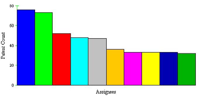
3 The Top 10 in Nanotech Patenting Univ Cal SAMSUNG IBM
4 The Folks Who Follow Me Thermal Management at the Nanoscale A. Balandin, University of California, Riverside, CA Nanostructure Materials for Lithium-Based Energy Storage N. Hudak, Sandia National Laboratories, Albuquerque, NM Development of Piezoelectric Nanocomposites for Energy Harvesting and Storage K. Loh, University of California, Davis, CA Manufacture of Nano Structures for Power Electronic Application B. Hunt, Etomate, Simi Valley, CA Nanoscale Catalyst-A Leapfrog Increase in Energy Storage K. McGrath, QuantumSphere, Santa Ana, CA

5 Nano-Enable Thermal Management Thermal copper bumps


6 Nextreme s OptoCooler module, the world s smallest thermoelectric cooler and the industry's first device to offer a heat pumping density in excess of 70 W/cm 2.
7 U.S. PAT. NO. Title 7,638,705 Thermoelectric generators for solar conversion and related systems and methods 7,523,617 Thin film thermoelectric devices for hot-spot thermal management in microprocessors and other electronics 7,342,496 RF-enabled pallet 7,342,169 Phonon-blocking, electrontransmitting low-dimensional structures *** 7,235,735 Thermoelectric devices utilizing double-sided Peltier junctions and methods of making the devices
8 U.S. Patent 7,342,169 Phonon- Blocking, Electron-Transmitting Low- Dimensional Structures

9 OptoCooler UPF40 Module
10 >6000 Thermoelectric U.S. Patents
11 Nanostructured Materials for Lithium-Based Energy Storage Electrodes Electrolytes Lithium Ion Batteries Fuel Cells Supercapacitors


12 Nanostructured Materials for Lithium-Based Energy Storage 144 U.S. Patents since 2005 Fullerene nanotubes by Smalley et al.

13 Nanoporous Silicon Electrodes 6-10X Higher Li ion capacity

14 Fuels Cells Nano Enables the Proton Exchange Membrane PEM

15 >250 Nano-enabled Fuel Cell PEM U.S. Patents Since 2005

16 n-abled Supercapacitors Prof. Yury Gogotsi, Drexel University, Phila., PA

17 ~100 n-abled Supercapacitor Issued U.S. Patents

18 Piezoelectric Nanocomposites for Energy Harvesting and Storage Prof. Z. L. Wang, Georgia Tech

19 Fiber-based Nanotechnology Could Power Electronic Devices "Power shirt would harvest energy from physical movement
20 22 n-abled Piezoelectric U.S. Patents The Boeing Company The Boeing Company The Boeing Company The Boeing Company The Boeing Company The Boeing Company The Boeing Company Schlumberger Rockwell Technologies Robert Bosch GmbH Ocean Power Technologies, Inc. NASA Strain energy shuttle apparatus and method for vibration energy harvesting Multi-frequency piezoelectric energy harvester Broadband energy harvester apparatus and method Energy harvesting apparatus and method Broadband energy harvester apparatus and method Single crystal piezo (SCP) apparatus and method of forming same High efficiency passive piezo energy harvesting apparatus Harvesting energy from flowing fluid Piezoelectric energy harvester and method Energy harvesting device manufactured by print forming processes Energy harvesting eel Hybrid piezoelectric energy harvesting transducer system
21
22 It s Tuesday!
23 17 Nanotech U.S. Patents Issued Today 3M Microporous article having metallic nanoparticle coating Canon Anelva Corporation Contour Semiconductor, Inc. Intel IBM IBM Toshiba Micron Technology, Inc. Nanoco, LLC NanoSembly, LLC Nanosilicon semiconductor substrate manufacturing Nano-vacuum-tubes and their application in storage devices Introducing nanotubes in trenches and structures formed thereby Magnetic racetrack with current-controlled motion of domain walls within an undulating energy landscape Non-volatile switching and memory devices using vertical nanotubes Magnetic memory Nanoscale floating gate and methods of formation Medical composition employing nanostructures Self assembled nanostructures and methods for preparing
24 Nanotech U.S. Patents Issued Today Nanosys, Inc. Nanowire capacitor and methods of making same Nanosys, Inc. Systems and methods for nanowire growth and harvesting Nantero, Inc. Aqueous carbon nanotube applicator liquids and methods for producing applicator liquids thereof Nantero, Inc. Isolated metal plug process for use in fabricating carbon nanotube memory cells Plasmet Corporation Continuous production of carbon nanomaterials using a high temperature inductively coupled plasma Harvard University Doped elongated semiconductors Univ. of Iowa / Univ. of Cal. Teleportation system for electronic many-qubit states using individual photons

25 U.S. Pat. No. 7,666,791, Issued 23 Feb 2010 Nanosys, Inc. Systems and methods for nanowire growth and harvesting
26 My Penultimate Slide Patent Claims Overlap! Energy Harvesting System Claims (owned by Company B) Where is your product? A nanowire (owned by Company B) Method of making nanowire (owned by Company A)

27 My Last Slide - Any Questions? GO USA!
OneD Material LLC - Patent Portfolio Overview
 OneD Material LLC - Patent Portfolio Overview List of Patents and Patent applications owned or licensed exclusively by OneD. Most of the inventions relate to nanostructure materials suitable for energy
ME 4875/MTE C16. Introduction to Nanomaterials and Nanotechnology. Lecture 2 - Applications of Nanomaterials + Projects
 ME 4875/MTE 575 - C16 Introduction to Nanomaterials and Nanotechnology Lecture 2 - Applications of Nanomaterials + Projects 1 Project Teams of 4 students each Literature review of one application of nanotechnology
Carbon Nanomaterials: Nanotubes and Nanobuds and Graphene towards new products 2030
 Carbon Nanomaterials: Nanotubes and Nanobuds and Graphene towards new products 2030 Prof. Dr. Esko I. Kauppinen Helsinki University of Technology (TKK) Espoo, Finland Forecast Seminar February 13, 2009
GRAPHENE: TECHNOLOGIES, APPLICATIONS AND MARKETS
 GRAPHENE: TECHNOLOGIES, APPLICATIONS AND MARKETS AVM075B July 2012 Andrew McWilliams Project Analyst ISBN: 0-89336-060-0 BCC Research 49 Walnut Park, Building 2 Wellesley, MA 02481 Phone: 866-285-7215
Research to Improve Photovoltaic (PV) Cell Efficiency by Hybrid Combination of PV and Thermoelectric Cell Elements.
 Cell Efficiency by Hybrid Combination of PV and Thermoelectric Cell Elements.") UNIVERSITY OF CENTRAL FLORIDA Research to Improve Photovoltaic (PV) Cell Efficiency by Hybrid Combination of PV and Thermoelectric Cell Elements. Page 129 PI: Nicoleta Sorloaica-Hickman, Robert Reedy Students:
UNIVERSITY OF CENTRAL FLORIDA Research to Improve Photovoltaic (PV) Cell Efficiency by Hybrid Combination of PV and Thermoelectric Cell Elements. Page 129 PI: Nicoleta Sorloaica-Hickman, Robert Reedy Students:
GRAPHENE: TECHNOLOGIES, APPLICATIONS AND MARKETS. AVM075C September Andrew McWilliams Project Analyst ISBN: X
 GRAPHENE: TECHNOLOGIES, APPLICATIONS AND MARKETS AVM075C September 2013 Andrew McWilliams Project Analyst ISBN: 1-56965-543-X BCC Research 49 Walnut Park, Building 2 Wellesley, MA 02481 866-285-7215, 781-489-7301
Scalable Nanomaterials and Nanostructures for Energy and Flexible Electronics
 Scalable Nanomaterials and Nanostructures for Energy and Flexible Electronics Liangbing (Bing) Hu MSE & Energy Center University of Maryland College Park Email: binghu@umd.edu 1 Transparent Paper from
Nanostrukturphysik (Nanostructure Physics)
") Nanostrukturphysik (Nanostructure Physics) Prof. Yong Lei & Dr. Yang Xu Fachgebiet 3D-Nanostrukturierung, Institut für Physik Contact: yong.lei@tu-ilmenau.de; yang.xu@tu-ilmenau.de Office: Unterpoerlitzer
Nanostrukturphysik (Nanostructure Physics) Prof. Yong Lei & Dr. Yang Xu Fachgebiet 3D-Nanostrukturierung, Institut für Physik Contact: yong.lei@tu-ilmenau.de; yang.xu@tu-ilmenau.de Office: Unterpoerlitzer
DocumentToPDF trial version, to remove this mark, please register this software.
 PAPER PRESENTATION ON Carbon Nanotube - Based Nonvolatile Random Access Memory AUTHORS M SIVARAM PRASAD Sivaram.443@gmail.com B N V PAVAN KUMAR pavankumar.bnv@gmail.com 1 Carbon Nanotube- Based Nonvolatile
Solutions for Assignment-8
 Solutions for Assignment-8 Q1. The process of adding impurities to a pure semiconductor is called: [1] (a) Mixing (b) Doping (c) Diffusing (d) None of the above In semiconductor production, doping intentionally
Research Grants Approved and Funded
 Research Grants Approved and Funded Koratkar has won 35 grants (totaling ~ $9.7 Million) from several agencies such as the National Science Foundation, Office of Naval Research, Army Research Office, Advanced
Global Intellectual Property Issues for Nanotechs:
 Global Intellectual Property Issues for Nanotechs: Applications and Standards Chinh H. Pham Greenberg Traurig, LLP (617) 310-6239 phamc@gtlaw.com www.gtlaw.com November 2005 1 GREENBERG TRAURIG, LLP ATTORNEYS
Commercial Graphene Applications: Current Research and Future Prospects
 Commercial Graphene Applications: Current Research and Future Prospects Overview History and Overview of Graphene Angstron Materials and Nanotek Instruments Applications of Graphene Thermal Management
NEW ELECTRONIC MATERIALS AND DEVICE TECHNOLOGIES: GLOBAL MARKETS
 NEW ELECTRONIC MATERIALS AND DEVICE TECHNOLOGIES: GLOBAL MARKETS AVM078B January 2017 Christopher Maara Project Analyst ISBN: 1-62296-423-3 BCC Research 49 Walnut Park, Building 2 Wellesley, MA 02481 USA
CHAPTER EIGHT: PHOTONIC CRYSTALS: MATERIALS, END USES, AND MARKETS, MATERIALS PROPERTIES... 78
 CHAPTER ONE: INTRODUCTION... 1 STUDY BACKGROUND... 1 STUDY GOALS AND OBJECTIVES... 1 INTENDED AUDIENCE... 2 SCOPE AND FORMAT... 2 INFORMATION SOURCES AND METHODOLOGY... 3 ANALYST CREDENTIALS... 4 RELATED
Optimization of MnO2 Electrodeposits using Graphenated Carbon Nanotube Electrodes for Supercapacitors
 Optimization of MnO2 Electrodeposits using Graphenated Carbon Nanotube Electrodes for Supercapacitors Waleed Nusrat, 100425398 PHY 3090U Material Science Thursday April 9 th 2015 Researchers optimize the
C- Mats and their Applications
 C- Mats and their Applications Materials and Electrochemical Research (MER) Corporation Tucson, Arizona Dr. R. O. LOUTFY MER HISTORY g MER is a private Arizona Corporation started in 1985 by Drs. R.O.Loutfy
materials, devices and systems through manipulation of matter at nanometer scale and exploitation of novel phenomena which arise because of the
 Nanotechnology is the creation of USEFUL/FUNCTIONAL materials, devices and systems through manipulation of matter at nanometer scale and exploitation of novel phenomena which arise because of the nanometer
Nanotechnology Fabrication Methods.
 Nanotechnology Fabrication Methods. 10 / 05 / 2016 1 Summary: 1.Introduction to Nanotechnology:...3 2.Nanotechnology Fabrication Methods:...5 2.1.Top-down Methods:...7 2.2.Bottom-up Methods:...16 3.Conclusions:...19
In today s lecture, we will cover:
 In today s lecture, we will cover: Metal and Metal oxide Nanoparticles Semiconductor Nanocrystals Carbon Nanotubes 1 Week 2: Nanoparticles Goals for this section Develop an understanding of the physical
RAJASTHAN TECHNICAL UNIVERSITY, KOTA
 RAJASTHAN TECHNICAL UNIVERSITY, KOTA (Electronics & Communication) Submitted By: LAKSHIKA SOMANI E&C II yr, IV sem. Session: 2007-08 Department of Electronics & Communication Geetanjali Institute of Technical
Nanostructure. Materials Growth Characterization Fabrication. More see Waser, chapter 2
 Nanostructure Materials Growth Characterization Fabrication More see Waser, chapter 2 Materials growth - deposition deposition gas solid Physical Vapor Deposition Chemical Vapor Deposition Physical Vapor
There's Plenty of Room at the Bottom
 There's Plenty of Room at the Bottom 12/29/1959 Feynman asked why not put the entire Encyclopedia Britannica (24 volumes) on a pin head (requires atomic scale recording). He proposed to use electron microscope
Materials Science and Engineering at Michigan State
 Materials Science and Engineering at Michigan State Material Science and Engineering Overview Material Engineering: applies chemistry, physics, biology, and mathematics to engineer atomic structure/architecture
Energy Storage. Light-emitting. Nano-Carbons. H 2 Energy. CNT synthesis. Graphene synthesis Top-down. Solar H 2 generation
 Nano-Carbon battery Graphene synthesis Top-down CNT synthesis CVD reactor hydrocarbon gas Catalyst CNTs Chemical Modification COO O NO 2 COO COO COO Bottom-up O O NO NO 2 2 COO COO Nano-Carbons 20 nm Light-emitting
PV Tutorial Allen Hermann, Ph. D. Professor of Physics Emeritus, and Professor of Music Adjunct, University of Colorado, Boulder, Colorado, USA and
 PV Tutorial Allen Hermann, Ph. D. Professor of Physics Emeritus, and Professor of Music Adjunct, University of Colorado, Boulder, Colorado, USA and Vice-president, NanoTech Inc. Lexington, Kentucky, USA
3/10/2013. Lecture #1. How small is Nano? (A movie) What is Nanotechnology? What is Nanoelectronics? What are Emerging Devices?
 What is Nanotechnology? What is Nanoelectronics? What are Emerging Devices?") EECS 498/598: Nanocircuits and Nanoarchitectures Lecture 1: Introduction to Nanotelectronic Devices (Sept. 5) Lectures 2: ITRS Nanoelectronics Road Map (Sept 7) Lecture 3: Nanodevices; Guest Lecture by
EECS 498/598: Nanocircuits and Nanoarchitectures Lecture 1: Introduction to Nanotelectronic Devices (Sept. 5) Lectures 2: ITRS Nanoelectronics Road Map (Sept 7) Lecture 3: Nanodevices; Guest Lecture by
Nano-mechatronics. Presented by: György BudaváriSzabó (X0LY4M)
") Nano-mechatronics Presented by: György BudaváriSzabó (X0LY4M) Nano-mechatronics Nano-mechatronics is currently used in broader spectra, ranging from basic applications in robotics, actuators, sensors,
Nano-mechatronics Presented by: György BudaváriSzabó (X0LY4M) Nano-mechatronics Nano-mechatronics is currently used in broader spectra, ranging from basic applications in robotics, actuators, sensors,
Index. batteries 150, 206, 219, 349, 355, rechargeable 139 biosensors 219 bulk materials 9, 19, 362 buoyancy
 Index absorption 262, 264, 325, 327, 346 absorption losses 259 60, 262, 264 activated carbons 76, 110, 115 16 granulated 115 16 adsorption 9 10, 80, 85, 88, 109, 111, 115 16, 278, 326 adsorption behavior
Materials and Structural Design for Advanced Energy Storage Devices
 Materials and Structural Design for Advanced Energy Storage Devices Imran Shakir Sustainable Energy Technologies Center (SET) King Saud University Saudi Arabia Specific Power (W/kg) Introduction and Motivation
ETH Rüschlikon the people and their research
 ETH Zurich @ Rüschlikon the people and their research Prof. Dr. Dimos Poulikakos, Laboratory of Thermodynamics in Emerging Technologies and Coordinator of the Nanotechnology Center, ETH Zurich The Vision
a succinct nanotechnology tutorial in four packets Nano Notions Remembered Nanotechnology Science Nanotechnology Research Nanotechnology Industry
 10-9 PSMA Nano 200 a succinct nanotechnology tutorial in four packets Nano Notions Remembered Nanotechnology Science Nanotechnology Research Nanotechnology Industry A Synopsis To View To Read Nano Review
Issued Patents Patent Applications
 Issued Patents Clemson Docket Number 00-002 00-002 00-002 00-011 01-001 01-004 01-016 01-016 01-027 01-034 02-002 02-002 03-003 03-028 03-030 04-012 04-029 04-037 05-006 05-015 05-027 05-027 06-009 06-044
Introduction. Energy Generation with the Piezo Effect
 Introduction The term Energy Harvesting is popularly used when electricity is generated from sources such as ambient temperature, vibrations or air flows. Since there are now electronic circuits whose
ENERGY NANOTECHNOLOGY --- A Few Examples
 ENERGY NANOTECHNOLOGY --- A Few Examples Gang Chen Nanoengineering Group Rohsenow Heat and Mass Transfer Laboratory Massachusetts Institute of Technology Cambridge, MA 02139 Email: gchen2@mit.edu http://web.mit.edu/nanoengineering
Functional Materials. Optical and Magnetic Applications. Electrical, Dielectric, Electromagnetic, Deborah D. L Chung.
 SINGAPORE Functional Materials Electrical, Dielectric, Electromagnetic, Optical and Magnetic Applications Deborah D. L Chung State University of New York at Buffalo, USAy^, NEW JERSEY LONDON ^ World Scientific
Nanotechnology and Solar Energy. Solar Electricity Photovoltaics. Fuel from the Sun Photosynthesis Biofuels Split Water Fuel Cells
 Nanotechnology and Solar Energy Solar Electricity Photovoltaics Fuel from the Sun Photosynthesis Biofuels Split Water Fuel Cells Solar cell A photon from the Sun generates an electron-hole pair in a semiconductor.
Lectures Graphene and
 Lectures 15-16 Graphene and carbon nanotubes Graphene is atomically thin crystal of carbon which is stronger than steel but flexible, is transparent for light, and conducts electricity (gapless semiconductor).
Challenges for Materials to Support Emerging Research Devices
 Challenges for Materials to Support Emerging Research Devices C. Michael Garner*, James Hutchby +, George Bourianoff*, and Victor Zhirnov + *Intel Corporation Santa Clara, CA + Semiconductor Research Corporation
Simple piezoresistive accelerometer
 Simple piezoresistive pressure sensor Simple piezoresistive accelerometer Simple capacitive accelerometer Cap wafer C(x)=C(x(a)) Cap wafer may be micromachined silicon, pyrex, Serves as over-range protection,
Synthesis of LiFePO 4 Nanostructures for Lithium-Ion Batteries by Electrochemical Deposition
 Synthesis of LiFePO 4 Nanostructures for Lithium-Ion Batteries by Electrochemical Deposition Erika Aragon and Alfredo A. Martinez-Morales Southern California Research Initiative for Solar Energy College
CURRICULUM VITAE HUAMIN LI UPDATED: DECEMBER 1, 2015 MAIN RESEARCH INTERESTS EDUCATION
 CURRICULUM VITAE HUAMIN LI UPDATED: DECEMBER 1, 2015 Postdoctoral Research Associate Center for Low Energy Systems Technology (LEAST), Department of Electrical Engineering University of Notre Dame, B20
The Patent Landscape of Silicon Nanowire Energy Storage Devices
 NANOTECHNOLOGY LAW & BUSINESS The Patent Landscape of Silicon Nanowire Energy Storage Devices Douglas Sharrott * and Erin J.D. Austin ** Abstract Lithium ion batteries are used in portable electronic devices,
Batteries: Now and Future
 Batteries: Now and Future Yi Cui Department of Materials Science and Engineering Stanford University Stanford Institute for Materials and Energy Sciences SLAC National Accelerator Laboratory Mobile Phone
Institut für Energie und Umwelttechnik e.v.
 Institut für Energie und Umwelttechnik e.v. Continuous synthesis of highly-specific nanopowder on the pilot-plant scale Tim Hülser Successful R&I 2015, Düsseldorf Duisburg, North-Rhine-Westphalia, Germany
APPLICATIONS OF NANOTECHNOLOGIES AND NANOMATERIALS
 APPLICATIONS OF NANOTECHNOLOGIES AND NANOMATERIALS Prof. G. P. VISSOKOV, Ph.D., D.Sc. MEMBER OF NATIONAL COORDINATION COUNSIL OF NANOTECHNOLOGIES INSTITUTE OF CATALYSIS BULGARIAN ACADEMY OF SCIENCES TEL:
EUROPEAN PATENT OFFICE U.S. PATENT AND TRADEMARK OFFICE CPC NOTICE OF CHANGES 270 DATE: NOVEMBER 1, 2016 PROJECT RP0259. Action Subclass Group(s)
") EUROPEAN PATENT OFFICE U.S. PATENT AND TRADEMARK OFFICE The following classification changes will be effected by this Notice of Changes: Action Subclass Group(s) Title wording changes: H01L 21/18 H01L
EUROPEAN PATENT OFFICE U.S. PATENT AND TRADEMARK OFFICE The following classification changes will be effected by this Notice of Changes: Action Subclass Group(s) Title wording changes: H01L 21/18 H01L
EN2912C: Future Directions in Computing Lecture 08: Overview of Near-Term Emerging Computing Technologies
 EN2912C: Future Directions in Computing Lecture 08: Overview of Near-Term Emerging Computing Technologies Prof. Sherief Reda Division of Engineering Brown University Fall 2008 1 Near-term emerging computing
Thermoelectric Energy Harvesting with Carbon Nanotube Systems
 Thermoelectric Energy Harvesting with Carbon Nanotube Systems Presented by Thomas C. Van Vechten, Ph.D. At the New England Nanomanufacturing Summit at UMass Lowell, June 2010 1 Outline Carbon Nanotubes
Monolithic Cells for Solar Fuels
 Electronic Supplementary Material (ESI) for Chemical Society Reviews. This journal is The Royal Society of Chemistry 2014 Monolithic Cells for Solar Fuels Jan Rongé, Tom Bosserez, David Martel, Carlo Nervi,
Graphene Fundamentals and Emergent Applications
 Graphene Fundamentals and Emergent Applications Jamie H. Warner Department of Materials University of Oxford Oxford, UK Franziska Schaffel Department of Materials University of Oxford Oxford, UK Alicja
CHAPTER 11 Semiconductor Theory and Devices
 CHAPTER 11 Semiconductor Theory and Devices 11.1 Band Theory of Solids 11.2 Semiconductor Theory 11.3 Semiconductor Devices 11.4 Nanotechnology It is evident that many years of research by a great many
RESEARCH METHODOLOGY EXECUTIVE SUMMARY Two-dimensional (2D) materials Graphene Short term opportunities...
 materials Graphene Short term opportunities...") Table of contents RESEARCH METHODOLOGY... 43 EXECUTIVE SUMMARY... 45 Two-dimensional (2D) materials... 45 Graphene... 46 Short term opportunities... 48 Medium-Long term opportunities... 48 Remarkable properties...
Table of contents RESEARCH METHODOLOGY... 43 EXECUTIVE SUMMARY... 45 Two-dimensional (2D) materials... 45 Graphene... 46 Short term opportunities... 48 Medium-Long term opportunities... 48 Remarkable properties...
Peltier Application Note
 Peltier Application Note Early 19th century scientists, Thomas Seebeck and Jean Peltier, first discovered the phenomena that are the basis for today s thermoelectric industry. Seebeck found that if you
e - Galvanic Cell 1. Voltage Sources 1.1 Polymer Electrolyte Membrane (PEM) Fuel Cell
 Fuel Cell") Galvanic cells convert different forms of energy (chemical fuel, sunlight, mechanical pressure, etc.) into electrical energy and heat. In this lecture, we are interested in some examples of galvanic cells.
Galvanic cells convert different forms of energy (chemical fuel, sunlight, mechanical pressure, etc.) into electrical energy and heat. In this lecture, we are interested in some examples of galvanic cells.
SELF-ASSEMBLY AND NANOTECHNOLOGY A Force Balance Approach
 SELF-ASSEMBLY AND NANOTECHNOLOGY A Force Balance Approach Yoon S. Lee Scientific Information Analyst Chemical Abstracts Service A Division of the American Chemical Society Columbus, Ohio WILEY A JOHN WILEY
NANO TECHNOLOGY IN POLYMER SOLAR CELLS. Mayur Padharia, Hardik Panchal, Keval Shah, *Neha Patni, Shibu.G.Pillai
 NANO TECHNOLOGY IN POLYMER SOLAR CELLS Mayur Padharia, Hardik Panchal, Keval Shah, *Neha Patni, Shibu.G.Pillai Department of Chemical Engineering, Institute of Technology, Nirma University, S. G. Highway,
Chemistry Instrumental Analysis Lecture 8. Chem 4631
 Chemistry 4631 Instrumental Analysis Lecture 8 UV to IR Components of Optical Basic components of spectroscopic instruments: stable source of radiant energy transparent container to hold sample device
POSEIDON SELECT IN SITU LIQUID ELECTRON MICROSCOPY. Protochips Quantifiably Better
 POSEIDON SELECT IN SITU LIQUID ELECTRON MICROSCOPY Protochips Quantifiably Better TiO 2 Nanoparticles 150 nm of water Image courtesy Dr. Madeline Dukes SEE THINGS IN LIQUID YOU NEVER THOUGHT POSSIBLE Pegylated
The Importance of Electrochemistry for the Development of Sustainable Mobility
 TUM CREATE Centre for Electromobility, Singapore The Importance of Electrochemistry for the Development of Sustainable Mobility Jochen Friedl, Ulrich Stimming DPG-Frühjahrstagung, Working Group on Energy,
state expose the the positive (electrode 2; top electrode S 1
 Supplementary Figure 1. Procedure for fabricatingg ENHANS ribbon. (a) All solid state symmetric supercapacitor, (b) supercapacitor after peeling off the paper cover from one of the copper tape electrodes
PHYS 3313 Section 001 Lecture #21 Monday, Nov. 26, 2012
 PHYS 3313 Section 001 Lecture #21 Monday, Nov. 26, 2012 Superconductivity Theory, The Cooper Pair Application of Superconductivity Semi-Conductor Nano-technology Graphene 1 Announcements Your presentations
Manufacture of Nanostructures for Power Electronics Applications
 Manufacture of Nanostructures for Power Electronics Applications Brian Hunt and Jon Lai Etamota Corporation 2672 E. Walnut St. Pasadena, CA 91107 APEC, Palm Springs Feb. 23rd, 2010 1 Background Outline
SPECIFIC USES OR APPLICATIONS OF NANOSTRUCTURES; MEASUREMENT OR ANALYSIS OF NANOSTRUCTURES; MANUFACTURE OR TREATMENT OF NANOSTRUCTURES
 CPC - B82Y - 2017.08 B82Y SPECIFIC USES OR APPLICATIONS OF NANOSTRUCTURES; MEASUREMENT OR ANALYSIS OF NANOSTRUCTURES; MANUFACTURE OR TREATMENT OF NANOSTRUCTURES Definition statement This place covers:
Micro/nano and precision manufacturing technologies and applications
 The 4th China-American Frontiers of Engineering Symposium Micro/nano and precision manufacturing technologies and applications Dazhi Wang School of Mechanical Engineering Dalian University of Technology
Solid State Physics (condensed matter): FERROELECTRICS
: FERROELECTRICS") Solid State Physics (condensed matter): FERROELECTRICS Prof. Igor Ostrovskii The University of Mississippi Department of Physics and Astronomy Oxford, UM: May, 2012 1 People: Solid State Physics Condensed
Solid State Physics (condensed matter): FERROELECTRICS Prof. Igor Ostrovskii The University of Mississippi Department of Physics and Astronomy Oxford, UM: May, 2012 1 People: Solid State Physics Condensed
Wire-shaped supercapacitor by hydrothermal self-assembly of graphene on copper wires
 Wire-shaped supercapacitor by hydrothermal self-assembly of graphene on copper wires Andrea Lamberti 22 September 2015 Outline Introduction Supercapacitors Wearable SCs Graphene Aerogels Synthesis Characterizations
Using the surface spontaneous depolarization field of ferroelectrics to direct the assembly of virus particles
 Appl. Phys. Lett. Vol 85, Issue 16, 3537 (2004) Using the surface spontaneous depolarization field of ferroelectrics to direct the assembly of virus particles Working Title: Directed assembly of biological
The Japan-China Workshop on materials and their Application in New Energy Devices
 The Japan-China Workshop on materials and their Application in New Energy Devices 4-8th Oct. 2017 at Kyushu Institute of Technology, Wakamatsu Campus, Kitakyushu, Japan The International Workshop Organizer
Chapter 7. Conclusion and Future Scope
 Chapter 7 Conclusion and Future Scope This chapter presents a summary of the work with concluding remarks for the research performed and reported in this thesis and then lays out the future scope pertaining
Variable capacitor energy harvesting based on polymer dielectric and composite electrode
 2.8.215 Variable capacitor energy harvesting based on polymer dielectric and composite electrode Robert Hahn 1*, Yuja Yang 1, Uwe Maaß 1, Leopold Georgi 2, Jörg Bauer 1, and K.- D. Lang 2 1 Fraunhofer
MEMS Piezoelectric Vibration Harvesting
 ENERGY HARVESTING: MEMS Piezoelectric Vibration Harvesting Thermoelectric Harvesting Lindsay Miller, Alic Chen, Dr. Yiping Zhu, Deepa Madan, Michael Nill, Dr. Rei Cheng Juang, Prof. Paul K. Wright & Prof.
Education. Research Interest. Honor and Awards. Curriculum Vitae HyungMo Jeong
 Curriculum Vitae HyungMo Jeong Current address: Post-doctoral researcher at Lawrence Berkeley National Laboratory and Department of Chemistry, UC Berkeley. 1 Cyclotron Road, Berkeley, California 94720
Gold Nanoparticles Floating Gate MISFET for Non-Volatile Memory Applications
 Gold Nanoparticles Floating Gate MISFET for Non-Volatile Memory Applications D. Tsoukalas, S. Kolliopoulou, P. Dimitrakis, P. Normand Institute of Microelectronics, NCSR Demokritos, Athens, Greece S. Paul,
Transistor and Integrated Circuits: History
 Course Objective Review and practice fundamental chemical engineering concepts (mass, energy, and momentum transport coupled with heterogeneous and homogeneous reactions and thermodynamics). Apply these
Electrochemical Deposition of Carbon Nanotubes from Organic Solutions
 University of Central Florida UCF Patents Patent Electrochemical Deposition of Carbon Nanotubes from Organic Solutions 7-6-2004 Lee Chow University of Central Florida Elvira Anoshkina University of Central
 Rechargeable Battery Materials Group Rechargeable Battery Materials Group aims for the realization of solid-state batteries with high reliability and lithium air batteries with ultimate capacities. URL
Course file PPY15204 Nanoscience and Nanomaterials Table of Contents
 Department Physics Nanotechnology : M.sc Physics Course file PPY15204 Table Contents Second Year MSc Physics (2015-2016 Regulation) Detailed Lesson Plan UNIT-I: INTRODUCTION TO NANOTECHNOLOGY History Importance
7. Carbon Nanotubes. 1. Overview: Global status market price 2. Types. 3. Properties. 4. Synthesis. MWNT / SWNT zig-zag / armchair / chiral
 7. Carbon Nanotubes 1. Overview: Global status market price 2. Types MWNT / SWNT zig-zag / armchair / chiral 3. Properties electrical others 4. Synthesis arc discharge / laser ablation / CVD 5. Applications
NANOELECTRONICS beyond CMOS
 NANOELECTRONICS beyond CMOS David Pulfrey 1 NNI definition of Nanotechnology 1-10 nm is better But Intel prefer... 2 Bourianoff04 1 3 Bourianoff04 4 Moravec04 2 Increasing the Integration Level functional
Nanotechnology. An Introduction
 Nanotechnology An Introduction Nanotechnology A new interdisciplinary field of science The study of systems at the nanoscale The use of tools at the nanoscale Building and applying structures that are
Council for Innovative Research Peer Review Research Publishing System
 TiO2- CuI Nanoparticle /Ru Solid State Dye-Sensitize Solar Cells Samer. Y. Al-Dabagh, Sudad. S. Ahmed Wasan. J. Taher ABSTRACT University of Baghdad,College of Science for women, Department of Physics.
Nanostrukturphysik (Nanostructure Physics)
") Nanostrukturphysik (Nanostructure Physics) Prof. Yong Lei & Dr. Yang Xu Fachgebiet 3D-Nanostrukturierung, Institut für Physik Contact: yong.lei@tu-ilmenau.de; yang.xu@tu-ilmenau.de Office: Unterpoerlitzer
Nanostrukturphysik (Nanostructure Physics) Prof. Yong Lei & Dr. Yang Xu Fachgebiet 3D-Nanostrukturierung, Institut für Physik Contact: yong.lei@tu-ilmenau.de; yang.xu@tu-ilmenau.de Office: Unterpoerlitzer
Practical 1P4 Energy Levels and Band Gaps
 Practical 1P4 Energy Levels and Band Gaps What you should learn from this practical Science This practical illustrates some of the points from the lecture course on Elementary Quantum Mechanics and Bonding
6. Computational Design of Energy-related Materials
 6. Computational Design of Energy-related Materials Contents 6.1 Atomistic Simulation Methods for Energy Materials 6.2 ab initio design of photovoltaic materials 6.3 Solid Ion Conductors for Fuel Cells
1. Introduction : 1.2 New properties:
 Nanodevices In Electronics Rakesh Kasaraneni(PID : 4672248) Department of Electrical Engineering EEL 5425 Introduction to Nanotechnology Florida International University Abstract : This paper describes
1. Nanotechnology & nanomaterials -- Functional nanomaterials enabled by nanotechnologies.
 Novel Nano-Engineered Semiconductors for Possible Photon Sources and Detectors NAI-CHANG YEH Department of Physics, California Institute of Technology 1. Nanotechnology & nanomaterials -- Functional nanomaterials
Enrico Lamanna Supervisor: Corrado Di Natale
 Enrico Lamanna Supervisor: Corrado Di Natale Energy Harvesting Energy Harvesting = the process of capturing minute amounts of energy naturally-occurring energy sources, accumulating them and storing them
Device 3D. 3D Device Simulator. Nano Scale Devices. Fin FET
 Device 3D 3D Device Simulator Device 3D is a physics based 3D device simulator for any device type and includes material properties for the commonly used semiconductor materials in use today. The physical
INDUCE NANOSTRUCTURES WITH ELECTRIC FIELDS
 INDUCE NANOSTRUCTURES WITH ELECTRIC FIELDS David Pei With special thanks to my advisor: Wei Lu Abstract This semester, I induced different nanoparticles with electric fields to observe their behavior under
SYLLABUS FINDING NANO Syllabus NanoSCI DISCOVERING NANOTECHNOLOGY AND CULTURE IN GERMANY
 1. Syllabus NanoSCI Course title: NanoSCI - Electronic Properties of Nanoengineered Materials Catalog description: Physics and technology of nanoengineered materials and devices. Semiconductor nanostructures.
Computational Materials Design and Discovery Energy and Electronic Applications Synthesis Structure Properties
 Computational Materials Design and Discovery Energy and Electronic Applications Synthesis Structure Properties Supercapacitors Rechargeable batteries Supercomputer Photocatalysts Fuel cell catalysts First
New Materials for the Forest Products Industry. Bruce Lyne KTH, Dept. Surface and Corrosion Science
 New Materials for the Forest Products Industry Bruce Lyne KTH, Dept. Surface and Corrosion Science S curves in music? Performance CDs Internet based? LPs Time S curves in joint replacement? Performance
Dynamization evolution of Dry Etch Tools in Semiconductor Device Fabrication Gordon Cameron Intel Corp (November 2005)
") Dynamization evolution of Dry Etch Tools in Semiconductor Device Fabrication Gordon Cameron Intel Corp (November 2005) Abstract Engineering Systems follow recognized trends of evolution; the main parameters
Dynamization evolution of Dry Etch Tools in Semiconductor Device Fabrication Gordon Cameron Intel Corp (November 2005) Abstract Engineering Systems follow recognized trends of evolution; the main parameters
Thermal Management at Nanoscale: Problems and Opportunities
 Thermal Management at Nanoscale: Problems and Opportunities Alexander A. Balandin Nano-Device Laboratory Department of Electrical Engineering and Materials Science and Engineering Program University of
Cross Reference Art Collection Class 977 NANOTECHNOLOGY (April 19, 2005)
") Cross Reference Art Collection Class 977 NANOTECHNOLOGY (April 19, 2005) 7200E NANOSTRUCTURE 7240D. Integrated with dissimilar structures on a common substrate 7355C.. Having biological material component
Cross Reference Art Collection Class 977 NANOTECHNOLOGY (April 19, 2005) 7200E NANOSTRUCTURE 7240D. Integrated with dissimilar structures on a common substrate 7355C.. Having biological material component
Title Single Row Nano-Tribological Printing: A novel additive manufacturing method for nanostructures
 Nano-Tribological Printing: A novel additive manufacturing method for nanostructures H.S. Khare, N.N. Gosvami, I. Lahouij, R.W. Carpick hkhare@seas.upenn.edu carpick@seas.upenn.edu carpick.seas.upenn.edu
Energy Conversion in the Peltier Device
 Laboratory exercise 4 Energy Conversion in the Peltier Device Preface The purpose of this exercise is to become familiar with the Peltier effect. Students will observe Peltier device working as a heat
Optical Filter Using Graphene/Graphene Oxide Thin Films
 Optical Filter Using Graphene/Graphene Oxide Thin Films Abhay Varghese Thomas Graduate Student Department of Mechanical, Aerospace and Nuclear Engineering Rensselaer Polytechnic Institute, Troy, NY, USA
Highly piezoelectric, thermal stable ferroelectrets from cyclic olefin copolymer. Yan Li, Hui Wang, Changchun Zeng ANTEC 2015, Orlando
 Highly piezoelectric, thermal stable ferroelectrets from cyclic olefin copolymer Yan Li, Hui Wang, Changchun Zeng ANTEC 2015, Orlando Content 1. Introduction 2. COC ferroelectret 3. Hybrid COC-PDMS ferroelectret