Spectral analysis of the angular distribution function of back reflectors for thin film silicon solar cells
|
|
|
- Rosalyn Moody
- 5 years ago
- Views:
Transcription
1 Spectral analysis of the angular distribution function of back reflectors for thin film silicon solar cells J. Escarré, F. Villar, J.M. Asensi, J. Bertomeu, J. Andreu CeRMAE - Departament de Física Aplicada i Òptica, Universitat de Barcelona, Av. Diagonal 647, Barcelona, Spain Abstract Nowadays, one of the most important challenges to enhance the efficiency of thin film silicon solar cells is to increase the short circuit intensity by means of optical confinement methods, such as textured back-reflector structures. In this work, two possible textured structures to be used as back reflectors for n-i-p solar cells have been optically analysed and compared to a smooth one by using a system which is able to measure the angular distribution function (ADF) of the scattered light in a wide spectral range ( nm). The accurate analysis of the ADF data corresponding to the reflector structures and to the µc-si:h films deposited onto them allows the optical losses due to the reflector absorption and its effectiveness in increasing light absorption in the µc-si:h layer, mainly at long wavelengths, to be quantified. 1. Introduction In c-si:h solar cells, optical confinement strategies are necessary to enhance the light absorption in the active layer of the cell. These strategies are preferable to increasing the thickness of the intrinsic layer as they avoid a reduction of the internal electric field and, consequently, the loss of collection efficiency. The generation of a random texture [1-2] or a periodic structure [3-4] in order to disperse the incoming light and increase its optical path inside the cell is the most usual approach. This can be done by texturing the TCO layers [5-6] or the substrate itself [7]. This is usually accompanied by the use of a back reflector layer both in substrate [8] and superstrate [9] structures. The study of the angular distribution function (ADF) of the light scattered by a textured surface is a powerful tool, enabling its influence on the optical behaviour of the solar cell to be studied
2 without building the whole device. This measurement is usually carried out at one or two fixed wavelengths [10]. Other studies show a dependency between the angular distribution of the scattered light and the relation between the RMS roughness and the wavelength [1]. The aim is to find a surface morphology which disperses the maximum amount of light with wavelengths between 600 and 1000 nm. In this work an experimental set up developed to determine the ADF of the light scattered by a rough surface in a wide spectral range (between 350 and 1050 nm) is presented. By using it, two kinds of textured back reflector structures were analysed before and after the deposition of a c-si:h layer. The results obtained with these reflectors are compared with those of a smooth one. 2. Experimental The spectral ADF measurements were carried out in a system that allows us to measure the light scattered by a rough surface. A mercury lamp was used as light source and the different wavelengths were selected by means of a double-grating monochromator. The light was guided into the system by an optical fibre and was then focused, crossing through the sample, on the detector in its initial point. The sample can rotate around its own axis to change the incident angle, and the detector rotates around the sample at a fixed distance. To correct eventual changes caused by instabilities of the lamp, a beam splitter and a fixed detector were used. Both detectors were silicon photodiodes with an active area of 16 mm 2. The light was chopped and the signals of both detectors were measured by two lock-in amplifiers. For an incident beam perpendicular to the sample, the ADF is determined by: ADF ( ) S( ) S Total where S(α) is the signal obtained at an angle α, S Total is the signal of the incident beam and ΔΩ is the solid angle of the detector. Angle α = 180º corresponds to specular reflection and α = 0º would correspond to the non-scattered transmitted beam.
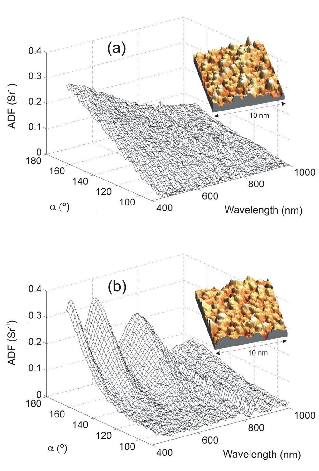
3 In the case of reflectors with random textures, revolution symmetry around the axis determined by the incident beam was assumed. This symmetry allowed us to determine all the scattered light by integrating the ADF from α =90º to values close to 180º. The specular reflection was then measured by slightly rotating the sample. From these measurements, the reflection haze parameter was calculated as the ratio of scattered light to total reflected light (scattered + specular). The absorption in the samples was estimated from 1-R, where R is the total reflectance (scattered + specular). In order to verify the accuracy of the system a Spectralon lambertian diffuser was measured and the result obtained (figure 1) showed a good agreement with the expected one for all the wavelengths used. The measurements carried out with this illumination system at a fixed wavelength of 633 nm matched with those obtained by using a red-diode laser. Three different back reflectors were studied. Back reflectors A and B consisted of a silver layer (50 nm) deposited respectively on a smooth substrate (Corning glass) and on a randomly textured substrate (commercially available Asahi-U substrate). Back reflector C was kindly offered by IPV Forschungzentrum Jülich, and consisted of a glass/ag/zno:al structure, where the ZnO:Al layer has been etched using HCl to obtain a nanometric roughness. An intrinsic c-si:h layer, with a thickness around 800 nm, was deposited by HWCVD on top of the three back reflectors. These samples were also optically analysed to observe the influence of these back reflector structures on the absorption of the silicon layer. 3. Results and Discussion The ADF of the scattered light for the back reflector structures B and C, and their AFM images are presented in figure 2. Both back reflectors exhibit a random texture with a RMS roughness of 28 nm for reflector B and 31 nm for reflector C. The measured RMS roughness for planar reflector (A) was 1 nm, and no scattered light was detected. For reflector B, the ADF did not present interferences and its shape was simply a consequence of the reflector morphology (figure 2a).
4 For the structure C, the ADF showed interferences due to the layer of ZnO:Al (figure 2b). The maxima in the scattered light were around 470, 570 and 750 nm and these corresponded to minima in the specular light. This fact indicates that, in spite of the light dispersion produced by the roughness, many of the photons were not scattered and their coherence was maintained giving interferences in the ZnO:Al layer. It is also important to point out that when the relation between the ADF and the morphology of a reflector has to be studied, a metallic layer should be the first surface in order to avoid interference effects, especially in the cases where the ADF measurement is done by using only a few wavelengths. The ADF of the back reflector C shows that the thickness of the ZnO:Al layer should play an important role to obtain a maximum in the scattered light around nm, which is the zone where a higher improvement of the optical behaviour of a solar cell can be obtained. Total diffuse light was calculated from the previous ADF, by assuming revolution symmetry. The haze reflection parameter obtained was very similar for both rough structures and its dependency with the wavelength is shown in figure 3. This fact certifies the narrow relation that exists between the morphology of a surface and the amount of light that it is able to scatter. Also a reduction of haze when increasing wavelength was observed for these reflectors, due to a loss in the scatter efficiency for their nanometric texture when the wavelength is increased. This fact shows the importance of considering the ratio between the RMS roughness and the wavelength in order to enhance the scattered light in the required spectral range. After deposition of a c-si:h layer on these reflectors, the RMS roughness values were 8 nm, 26 nm and 34 nm for the reflectors A, B and C respectively. Only the sample on the smooth reflector showed a significant increase in its roughness. This increase is due to the silicon microstructure which is smaller than the approximately 30 nm obtained for reflectors B and C. For this reason, no significant changes have been obtained in the morphology for reflectors B and C with the silicon layer on top. The ADF corresponding to these samples presented interferences which were related to the c-si:h layer. From these measurements, an estimation of the light absorbed in the silicon film
5 on the three back reflectors can be made (figure 4). In addition to 1 R curves corresponding to the reflector/si structures, those corresponding to the back reflectors are also presented. The absorption of the rough reflector B was higher than the one obtained for reflector A, specially, for the wavelengths between 450 and 600 nm. This fact has also been reported in other studies [11] and a similar increase in the absorption of rough silver layers respect to smooth ones has been measured by means of Photothermal Deflection Spectroscopy (PDS) [12]. For reflector C, the highest absorption was obtained in the short wavelength region of the spectra, decreasing to 0.3 around 850 nm. This high absorption is due to the optical confinement which takes place inside the ZnO:Al layer. Thus, when a photon is scattered with an angle higher than the limit one (ZnO:Al/air interface) it remains caught inside the TCO layer until it is absorbed. For this reason, the measured 1 R decreased as a function of the scattered light and the higher absorption was obtained for shorter wavelengths, where scattering is higher. However, this optical confinement inside the TCO layer would not take place in the whole device because the refraction index of the silicon is higher than the ZnO:Al one. Also, although the absorption of the back reflector would remain high in the spectral range from 350 nm to 600 nm, it will not be important because the majority of photons with these wavelengths should be totally absorbed in the active layer of the solar cell. For the three back reflectors with the silicon layer on top, similar absorption values were obtained at short wavelengths. At longer wavelengths, absorption in the silicon samples deposited onto rough reflectors (B and C) was very similar and considerably higher than that of the sample on the smooth back reflector. For instance, the mean values of 1 R for a-si:h samples on structures A and B in the region between 900 and 1000 nm were around 0.1 and 0.7, respectively. This important increase in the absorption has to take place in the silicon layer because the measured absorption for both back reflectors was around 0.01 in that wavelength range. This fact along with the high absorption obtained for the reflector C, with or without silicon, indicates that the used nanometric texture is really optimal for optical confinement. In spite of these high values of 1 R in the near infrared region, which agree with those obtained for solar cells with similar thicknesses [13], the quantum efficiency of the solar cells obtained
6 using this kind of technology is not greater than 0.1 for the wavelengths near to 1000 nm [14]. These important losses can be explained by means of the important absorption which takes place in the TCO and doped layers. 4. Conclusions In this work a system able to measure the ADF of the scattered light quantitatively in a wide spectral range has been presented. This setup has been used to study the optical behaviour of three different back reflectors and their influence on the absorption of a thin c-si:h layer. For the reflector that consisted in a rough silver layer, a higher absorption than for the smooth one has been obtained. The highest absorption has been measured for the reflector with a TCO layer on top. After the deposition of the c-si:h layer a higher absorption in the near infrared region is observed for both samples on rough reflectors. This indicates that the nanometric texture tested is really optimal for the optical confinement. Nevertheless, the low values usually attained for the quantum efficiency in that region compared to the absorption in the films point out that the TCO and doped layers are also key issues for the optical optimisation of the devices. Acknowledgements The authors thank Dr. Bern Rech from IPV Forschungzentrum Jülich for kindly supplying the glass/ag/zno:al back reflector. This work was supported by the Spanish Government (ENE C03-01/ALT).
7 References [1] O. Kluth, C. Zahren, H. Stiebig, B. Rech and H. Schade, Proceedings of 19 th European Photovoltaic Solar Energy Conference and Exhibition, Paris, 2004, Vol. II, p [2] J. Escarré, F. Villar, M. Fonrodona, D. Soler, J.M. Asensi, J. Bertomeu, J. Andreu, Proceedings of 19 th European Photovoltaic Solar Energy Conference and Exhibition, Paris, 2004, Vol. II, p [3] C. Eisele, C.E. Nebel, M. Stutzmann, J. Appl. Phys. 89 (2001) [4] N. Senoussaoui, M. Krause, J. Müller, E. Bunte, T. Brammer, H. Stiebig, Thin Solid Films (2004) [5] O. Kluth, B. Rech, L. Houben, S. Wieder, G. Schöpe, C. Beneking, H. Wagner, A. Löffl, H.W. Schock, Thin Solid Films 351 (1999) [6] J. Müller, G. Schöpe, O. Kluth, B. Rech, M. Ruske, J. Trube, B. Szyszka, X. Jiang, G. Bräuer, Thin Solid Films 392 (2001) [7] N. Chuansuwanich, P.I. Widenborg, P. Campbell, A.G. Aberle, Tech. Digest 14 th International Photovoltaic Science and Engineering Conference, Bangkok, 2004, p [8] T. Brammer, W. Reetz, N. Senoussaoui, O. Vetterl, O. Kluth, B. Rech, H. Stiebig, H. Wagner, Sol. Energy Mater. Sol. Cells 74 (2002) [9] J. Müller, B. Rech, J. Springer, M. Vanecek, Solar Energy 77 (2004) [10] J. Krc, M. Zeman, O. Kluth, F. Smole, M. Topic, Thin Solid Films 426 (2003) [11] D. Beaglehole, O. Hunderi, Phys. Rev. B 2 (1970) [12] J. Springer, A. Poruba, L. Müllerova, M.Vanecek, O. Kluth, B. Rech, J. Appl. Phys. 95 (2004) [13] J. Springer, B. Rech, W. Reetz, J. Müller, M. Vanecek, Sol. Energy Mater. Sol. Cells 85 (2005) [14] K. Yamamoto, M. Yoshimi, Y. Tawada, Y. Okamoto, A. Nakajima, Sol. Energy Mater. Sol. Cells 66 (2001)
8 Figure captions Figure 1. Measured angular distribution function (ADF) of the Spectralon lambertian diffuser from 400 to 1000 nm (a) and the comparison of its ADF with the expected one for an ideal lambertian diffuser at a wavelength of 600 nm (b). Figure 2. ADF and AFM images for reflector structure B (a) and for reflector structure C (b). Figure 3. Measured spectral dependencies of the haze parameters for reflector structures B and C. Figure 4. Absorption values for the three studied reflectors (open symbols) and for the corresponding reflector c-si:h structures (full symbols). The results for the structures A, B and C are represented in (a), (b) and (c) respectively.
9
10
11
12
OPTO-ELECTRONIC MODELLING OF THIN FILM NANOCRYSTALLINE SILICON SOLAR CELLS
 Journal of Ovonic Research Vol. 8, No. 4, July - August 2012, p. 81-90 OPTO-ELECTRONIC MODELLING OF THIN FILM NANOCRYSTALLINE SILICON SOLAR CELLS S.N. AGBO a, P.E. UGWUOKE a, F.I. EZEMA b a National Centre
Influence of front and back grating on light trapping in microcrystalline thin-film silicon solar cells
 Influence of front and back grating on light trapping in microcrystalline thin-film silicon solar cells Darin Madzharov, Rahul Dewan, and Dietmar Knipp* School of Engineering and Science, Electronic Devices
6 Correlation between the surface morphology and the current enhancement in n-i-p silicon solar cells
 6 Correlation between the surface morphology and the current enhancement in n-i-p silicon solar cells 6.1 Introduction In order to enhance the generated photocurrent in thin microcrystalline silicon solar
Infrared characterization of a-si:h/a-si1-xc x:h interfaces
 Infrared characterization of a-si:h/a-si1-xc x:h interfaces J. Bertomeu, J. Puigdollers, J.M. Asensi and J. Andreu. Laboratori de Física de Capes fines (LCFC), Departament de Física Aplicada i Electrònica,
Development of two-step etching approach for aluminum doped zinc. oxide using a combination of standard HCl and NH 4 Cl etch steps
 Development of two-step etching approach for aluminum doped zinc oxide using a combination of standard HCl and NH 4 Cl etch steps S. Fernández a), S.E. Pust b),j. Hüpkes b), F.B. Naranjo c) a) CIEMAT,
Optical Properties of Thin Semiconductor Films
 Optical Properties of Thin Semiconductor Films Grolik Benno,KoppJoachim October, 31st 2003 1 Introduction Optical experiments provide a good way of examining the properties of semiconductors. Particulary
Light trapping in thin-film solar cells: the role of guided modes
 Light trapping in thin-film solar cells: the role of guided modes T. Søndergaard *, Y.-C. Tsao, T. G. Pedersen, and K. Pedersen Department of Physics and Nanotechnology, Aalborg University, Skjernvej 4A,
PLASMONIC LIGHT TRAPPING FOR THIN FILM A-SI:H SOLAR CELLS
 PLASMONIC LIGHT TRAPPING FOR THIN FILM A-SI:H SOLAR CELLS VIVIAN E. FERRY 1,2, MARC A. VERSCHUUREN 3, HONGBO B. T. LI 4, EWOLD VERHAGEN 1, ROBERT J. WALTERS 1, RUUD E. I. SCHROPP 4, HARRY A. ATWATER 2,
Uwe Rau Institut für Energieforschung 5 Photovoltaik- Forschungszentrum Jülich GmbH
 Mitglied der Helmholtz-Gemeinschaft Materialforschung für f r DünnschichtphotovoltaikD nnschichtphotovoltaik- Status und neue Entwicklungen Uwe Rau Institut für Energieforschung 5 Photovoltaik- Forschungszentrum
OPTI510R: Photonics. Khanh Kieu College of Optical Sciences, University of Arizona Meinel building R.626
 OPTI510R: Photonics Khanh Kieu College of Optical Sciences, University of Arizona kkieu@optics.arizona.edu Meinel building R.626 Announcements Homework #6 is assigned, due May 1 st Final exam May 8, 10:30-12:30pm
OPTICAL ANALYSIS OF ZnO THIN FILMS USING SPECTROSCOPIC ELLIPSOMETRY AND REFLECTOMETRY.
 OPTICAL ANALYSIS OF ZnO THIN FILMS USING SPECTROSCOPIC ELLIPSOMETRY AND REFLECTOMETRY Katarína Bombarová 1, Juraj Chlpík 1,2, Soňa Flickyngerová 3, Ivan Novotný 3, Július Cirák 1 1 Institute of Nuclear
COMPARISON OF VHF, RF AND DC PLASMA EXCITATION FOR a-si:h DEPOSITION WITH HYDROGEN DILUTION
 COMPARISON OF, RF AND PLASMA EXCITATION FOR a-si:h DEPOSITION WITH HYDROGEN DILUTION R. PLATZ, C. HOF, S. WIEDER, B. RECH, D. FISCHER, A. SHAH, A. PAYNE and S. WAGNER Department of Electrical Engineering,
Nanophotonics: solar and thermal applications
 Nanophotonics: solar and thermal applications Shanhui Fan Ginzton Laboratory and Department of Electrical Engineering Stanford University http://www.stanford.edu/~shanhui Nanophotonic Structures Photonic
Lecture 0. NC State University
 Chemistry 736 Lecture 0 Overview NC State University Overview of Spectroscopy Electronic states and energies Transitions between states Absorption and emission Electronic spectroscopy Instrumentation Concepts
Model Answer (Paper code: AR-7112) M. Sc. (Physics) IV Semester Paper I: Laser Physics and Spectroscopy
 M. Sc. (Physics) IV Semester Paper I: Laser Physics and Spectroscopy") Model Answer (Paper code: AR-7112) M. Sc. (Physics) IV Semester Paper I: Laser Physics and Spectroscopy Section I Q1. Answer (i) (b) (ii) (d) (iii) (c) (iv) (c) (v) (a) (vi) (b) (vii) (b) (viii) (a) (ix)
Model Answer (Paper code: AR-7112) M. Sc. (Physics) IV Semester Paper I: Laser Physics and Spectroscopy Section I Q1. Answer (i) (b) (ii) (d) (iii) (c) (iv) (c) (v) (a) (vi) (b) (vii) (b) (viii) (a) (ix)
Because light behaves like a wave, we can describe it in one of two ways by its wavelength or by its frequency.
 Light We can use different terms to describe light: Color Wavelength Frequency Light is composed of electromagnetic waves that travel through some medium. The properties of the medium determine how light
Chemistry Instrumental Analysis Lecture 15. Chem 4631
 Chemistry 4631 Instrumental Analysis Lecture 15 IR Instruments Types of Instrumentation Dispersive Spectrophotometers (gratings) Fourier transform spectrometers (interferometer) Single beam Double beam
Scintillation Detectors
 Scintillation Detectors J.L. Tain Jose.Luis.Tain@ific.uv.es http://ific.uv.es/gamma/ Instituto de Física Corpuscular C.S.I.C - Univ. Valencia Scintillation detector: SCINTILLATION MATERIAL LIGHT-GUIDE
Integrating Spheres in Molecular Spectrophotometry
 Integrating Spheres in Molecular Spectrophotometry Theory and Practice 2012 Perkin Elmer 2012 Perkin Elmer General Sphere Theory 3 Integrating Spheres Types of Sphere Measurements Total Reflectance (Specular
Chapter 35 Diffraction and Polarization. Copyright 2009 Pearson Education, Inc.
 Chapter 35 Diffraction and Polarization 35-1 Diffraction by a Single Slit or Disk If light is a wave, it will diffract around a single slit or obstacle. 35-1 Diffraction by a Single Slit or Disk The resulting
PHOTOVOLTAICS Fundamentals
 PHOTOVOLTAICS Fundamentals PV FUNDAMENTALS Semiconductor basics pn junction Solar cell operation Design of silicon solar cell SEMICONDUCTOR BASICS Allowed energy bands Valence and conduction band Fermi
6. Plasmon coupling between a flat gold interface and gold nanoparticles.
 6. Plasmon coupling between a flat gold interface and gold nanoparticles. 6.1. Introduction In this outlook oriented chapter the applicability of the multilayered system used in chapter 4.1., for the study
Research Article Enhanced Light Trapping in Thin Film Solar Cells Using a Plasmonic Fishnet Structure
 Photoenergy Volume 25, Article ID 969, 8 pages http://dx.doi.org/.55/25/969 Research Article Enhanced Light Trapping in Thin Film Solar Cells Using a Plasmonic Fishnet Structure Sayan Seal, Vinay Budhraja,
OPTICAL Optical properties of multilayer systems by computer modeling
 Workshop on "Physics for Renewable Energy" October 17-29, 2005 301/1679-15 "Optical Properties of Multilayer Systems by Computer Modeling" E. Centurioni CNR/IMM AREA Science Park - Bologna Italy OPTICAL
Comparison between periodic and stochastic parabolic light trapping structures for thin-film microcrystalline Silicon solar cells
 Comparison between periodic and stochastic parabolic light trapping structures for thin-film microcrystalline Silicon solar cells M. Peters, 1,2,* C. Battaglia, 3 K. Forberich, 1 B. Bläsi, 2 N. Sahraei,
Near-Infrared Spectroscopy of Nitride Heterostructures EMILY FINAN ADVISOR: DR. OANA MALIS PURDUE UNIVERSITY REU PROGRAM AUGUST 2, 2012
 Near-Infrared Spectroscopy of Nitride Heterostructures EMILY FINAN ADVISOR: DR. OANA MALIS PURDUE UNIVERSITY REU PROGRAM AUGUST 2, 2012 Introduction Experimental Condensed Matter Research Study of large
Q. Shen 1,2) and T. Toyoda 1,2)
 and T. Toyoda 1,2)") Photosensitization of nanostructured TiO 2 electrodes with CdSe quntum dots: effects of microstructure in substrates Q. Shen 1,2) and T. Toyoda 1,2) Department of Applied Physics and Chemistry 1), and
Photosensitization of nanostructured TiO 2 electrodes with CdSe quntum dots: effects of microstructure in substrates Q. Shen 1,2) and T. Toyoda 1,2) Department of Applied Physics and Chemistry 1), and
PHYSICS nd TERM Outline Notes (continued)
") PHYSICS 2800 2 nd TERM Outline Notes (continued) Section 6. Optical Properties (see also textbook, chapter 15) This section will be concerned with how electromagnetic radiation (visible light, in particular)
PHYSICS 2800 2 nd TERM Outline Notes (continued) Section 6. Optical Properties (see also textbook, chapter 15) This section will be concerned with how electromagnetic radiation (visible light, in particular)
EUV Reflectivity measurements on Acktar Sample Magic Black
 Report EUV Reflectivity measurements on Acktar Sample Magic Black S. Döring, Dr. K. Mann Laser-Laboratorium Göttingen e.v. October 28, 2011 Contents 1 Introduction 3 2 Setup 3 3 Measurements 4 4 Conclusion
25 Instruments for Optical Spectrometry
 25 Instruments for Optical Spectrometry 25A INSTRUMENT COMPONENTS (1) source of radiant energy (2) wavelength selector (3) sample container (4) detector (5) signal processor and readout (a) (b) (c) Fig.
Photoluminescence emission through thin metal films via coupled surface plasmon polaritons
 Journal of Modern Optics Vol. 52, No. 6, 15 April 2005, 833 843 Photoluminescence emission through thin metal films via coupled surface plasmon polaritons S. WEDGE*y, S. H. GARRETTy, I. SAGEz and W. L.
Supplementary Information for. Vibrational Spectroscopy at Electrolyte Electrode Interfaces with Graphene Gratings
 Supplementary Information for Vibrational Spectroscopy at Electrolyte Electrode Interfaces with Graphene Gratings Supplementary Figure 1. Simulated from pristine graphene gratings at different Fermi energy
Practical 1P4 Energy Levels and Band Gaps
 Practical 1P4 Energy Levels and Band Gaps What you should learn from this practical Science This practical illustrates some of the points from the lecture course on Elementary Quantum Mechanics and Bonding
Practical 1P4 Energy Levels and Band Gaps
 Practical 1P4 Energy Levels and Band Gaps What you should learn from this practical Science This practical illustrates some of the points from the lecture course on Elementary Quantum Mechanics and Bonding
Materials Science and Engineering B
 Materials Science and Engineering B 178 (2013) 630 634 Contents lists available at SciVerse ScienceDirect Materials Science and Engineering B j o ur nal homep age: www.elsevier.com/locate/mseb Short communication
Available online at ScienceDirect. Energy Procedia 92 (2016 ) 24 28
 24 28") Available online at www.sciencedirect.com ScienceDirect Energy Procedia 92 (2016 ) 24 28 6th International Conference on Silicon Photovoltaics, SiliconPV 2016 Laplacian PL image evaluation implying correction
Available online at www.sciencedirect.com ScienceDirect Energy Procedia 92 (2016 ) 24 28 6th International Conference on Silicon Photovoltaics, SiliconPV 2016 Laplacian PL image evaluation implying correction
In-situ Multilayer Film Growth Characterization by Brewster Angle Reflectance Differential Spectroscopy
 In-situ Multilayer Film Growth Characterization by Brewster Angle Reflectance Differential Spectroscopy N. Dietz, D.J. Stephens, G. Lucovsky and K.J. Bachmann North Carolina State University, Raleigh,
Lecture 7: Optical Spectroscopy. Astrophysical Spectroscopy. Broadband Filters. Fabry-Perot Filters. Interference Filters. Prism Spectrograph
 Lecture 7: Optical Spectroscopy Outline 1 Astrophysical Spectroscopy 2 Broadband Filters 3 Fabry-Perot Filters 4 Interference Filters 5 Prism Spectrograph 6 Grating Spectrograph 7 Fourier Transform Spectrometer
Photogating effect observed in microcrystalline silicon solar cells and its applications in cell optimization
 6 Photogating effect observed in microcrystalline silicon solar cells and its applications in cell optimization As we discussed in the previous Chapters, quantum efficiency measurement is of great importance
Aluminum for nonlinear plasmonics: Methods Section
 Aluminum for nonlinear plasmonics: Methods Section Marta Castro-Lopez, Daan Brinks, Riccardo Sapienza, and Niek F. van Hulst, ICFO - Institut de Ciencies Fotoniques, and ICREA - Institució Catalana de
Supporting Information
 Electronic Supplementary Material (ESI) for Journal of Materials Chemistry A. This journal is The Royal Society of Chemistry 2018 Supporting Information A minimal non-radiative recombination loss for efficient
PHYS 4400, Principles and Varieties of Solar Energy Instructor: Randy J. Ellingson The University of Toledo
 Light and Photons PHYS 4400, Principles and Varieties of Solar Energy Instructor: Randy J. Ellingson The University of Toledo January 16, 2014 Light What is light? Electromagnetic wave direction of the
Vibrational Spectroscopies. C-874 University of Delaware
 Vibrational Spectroscopies C-874 University of Delaware Vibrational Spectroscopies..everything that living things do can be understood in terms of the jigglings and wigglings of atoms.. R. P. Feymann Vibrational
Highly Efficient and Anomalous Charge Transfer in van der Waals Trilayer Semiconductors
 Highly Efficient and Anomalous Charge Transfer in van der Waals Trilayer Semiconductors Frank Ceballos 1, Ming-Gang Ju 2 Samuel D. Lane 1, Xiao Cheng Zeng 2 & Hui Zhao 1 1 Department of Physics and Astronomy,
Regular Reflectance and Transmittance Measurements of Transmissive Materials Using a STAR GEM Optical Accessory
 Regular Reflectance and Transmittance Measurements of Transmissive Materials Using a STAR GEM Optical Accessory 1,3 E.Kawate, 1,2 M.Hain 1 AIST, 1-1-1, Central 2, Umezono, Tsukuba, Ibaraki 305-8568, Japan
Infrared Charge-Modulation Spectroscopy of Defects in Phosphorus Doped Amorphous Silicon
 Syracuse University SURFACE Physics College of Arts and Sciences 22 Infrared Charge-Modulation Spectroscopy of Defects in Phosphorus Doped Amorphous Silicon Kai Zhu Syracuse University Eric A. Schiff Syracuse
Reflectivity and photoluminescence studies in Bragg reflectors with absorbing layers
 INSTITUTE OF PHYSICS PUBLISHING SEMICONDUCTOR SCIENCE AND TECHNOLOGY Semicond. Sci. Technol. 16 (2001) 548 552 www.iop.org/journals/ss PII: S0268-1242(01)16119-5 Reflectivity and photoluminescence studies
Gratings in Electrooptic Polymer Devices
 Gratings in Electrooptic Polymer Devices Venkata N.P.Sivashankar 1, Edward M. McKenna 2 and Alan R.Mickelson 3 Department of Electrical and Computer Engineering, University of Colorado at Boulder, Boulder,
Chapter 35 Diffraction and Polarization
 Chapter 35 Diffraction and Polarization If light is a wave, it will diffract around a single slit or obstacle. The resulting pattern of light and dark stripes is called a diffraction pattern. This pattern
Fall 2014 Nobby Kobayashi (Based on the notes by E.D.H Green and E.L Allen, SJSU) 1.0 Learning Objectives
 1.0 Learning Objectives") University of California at Santa Cruz Electrical Engineering Department EE-145L: Properties of Materials Laboratory Lab 7: Optical Absorption, Photoluminescence Fall 2014 Nobby Kobayashi (Based on the
University of California at Santa Cruz Electrical Engineering Department EE-145L: Properties of Materials Laboratory Lab 7: Optical Absorption, Photoluminescence Fall 2014 Nobby Kobayashi (Based on the
Chapter 24 Photonics Question 1 Question 2 Question 3 Question 4 Question 5
 Chapter 24 Photonics Data throughout this chapter: e = 1.6 10 19 C; h = 6.63 10 34 Js (or 4.14 10 15 ev s); m e = 9.1 10 31 kg; c = 3.0 10 8 m s 1 Question 1 Visible light has a range of photons with wavelengths
Widely Tunable and Intense Mid-Infrared PL Emission from Epitaxial Pb(Sr)Te Quantum Dots in a CdTe Matrix
Te Quantum Dots in a CdTe Matrix") Widely Tunable and Intense Mid-Infrared PL Emission from Epitaxial Pb(Sr)Te Quantum Dots in a Matrix S. Kriechbaumer 1, T. Schwarzl 1, H. Groiss 1, W. Heiss 1, F. Schäffler 1,T. Wojtowicz 2, K. Koike 3,
Widely Tunable and Intense Mid-Infrared PL Emission from Epitaxial Pb(Sr)Te Quantum Dots in a Matrix S. Kriechbaumer 1, T. Schwarzl 1, H. Groiss 1, W. Heiss 1, F. Schäffler 1,T. Wojtowicz 2, K. Koike 3,
Design and Development of a Smartphone Based Visible Spectrophotometer for Analytical Applications
 Design and Development of a Smartphone Based Visible Spectrophotometer for Analytical Applications Bedanta Kr. Deka, D. Thakuria, H. Bora and S. Banerjee # Department of Physicis, B. Borooah College, Ulubari,
Nanocomposite photonic crystal devices
 Nanocomposite photonic crystal devices Xiaoyong Hu, Cuicui Lu, Yulan Fu, Yu Zhu, Yingbo Zhang, Hong Yang, Qihuang Gong Department of Physics, Peking University, Beijing, P. R. China Contents Motivation
Ultra-narrow-band tunable laserline notch filter
 Appl Phys B (2009) 95: 597 601 DOI 10.1007/s00340-009-3447-6 Ultra-narrow-band tunable laserline notch filter C. Moser F. Havermeyer Received: 5 December 2008 / Revised version: 2 February 2009 / Published
Temperature Dependent Optical Band Gap Measurements of III-V films by Low Temperature Photoluminescence Spectroscopy
 Temperature Dependent Optical Band Gap Measurements of III-V films by Low Temperature Photoluminescence Spectroscopy Linda M. Casson, Francis Ndi and Eric Teboul HORIBA Scientific, 3880 Park Avenue, Edison,
Highly Efficient Planar Perovskite Solar Cells through Band Alignment Engineering
 Electronic Supplementary Material (ESI) for Energy & Environmental Science. This journal is The Royal Society of Chemistry 2015 Highly Efficient Planar Perovskite Solar Cells through Band Alignment Engineering
Plasmonic Photovoltaics Harry A. Atwater California Institute of Technology
 Plasmonic Photovoltaics Harry A. Atwater California Institute of Technology Surface plasmon polaritons and localized surface plasmons Plasmon propagation and absorption at metal-semiconductor interfaces
THE ROLE OF FRONT ELECTRODES AND
 THE ROLE OF FRONT ELECTRODES AND INTERMEDIATE REFLECTORS IN THE OPTOELECTRONIC PROPERTIES OF HIGH-EFFICIENCY MICROMORPH SOLAR CELLS Thèse présentée à la Faculté des Sciences Institut de Microtechnique
Raman and stimulated Raman spectroscopy of chlorinated hydrocarbons
 Department of Chemistry Physical Chemistry Göteborg University KEN140 Spektroskopi Raman and stimulated Raman spectroscopy of chlorinated hydrocarbons WARNING! The laser gives a pulsed very energetic and
Relation between substrate surface morphology and microcrystalline silicon solar cell performance
 Published in Journal of Non-Crystalline Solids 354, 19-25, 2008 which should be used for any reference to this work 1 Relation between substrate surface morphology and microcrystalline silicon solar cell
Dept. of Physics, MIT Manipal 1
 Chapter 1: Optics 1. In the phenomenon of interference, there is A Annihilation of light energy B Addition of energy C Redistribution energy D Creation of energy 2. Interference fringes are obtained using
Skoog Chapter 6 Introduction to Spectrometric Methods
 Skoog Chapter 6 Introduction to Spectrometric Methods General Properties of Electromagnetic Radiation (EM) Wave Properties of EM Quantum Mechanical Properties of EM Quantitative Aspects of Spectrochemical
Supplementary Information. Light Manipulation for Organic Optoelectronics Using Bio-inspired Moth's Eye. Nanostructures
 Supplementary Information Light Manipulation for Organic Optoelectronics Using Bio-inspired Moth's Eye Nanostructures Lei Zhou, Qing-Dong Ou, Jing-De Chen, Su Shen, Jian-Xin Tang,* Yan-Qing Li,* and Shuit-Tong
Plasmonic Hot Hole Generation by Interband Transition in Gold-Polyaniline
 Supplementary Information Plasmonic Hot Hole Generation by Interband Transition in Gold-Polyaniline Tapan Barman, Amreen A. Hussain, Bikash Sharma, Arup R. Pal* Plasma Nanotech Lab, Physical Sciences Division,
Supplementary Figures
 Supplementary Figures Supplementary Figure 1. AFM profiles of the charge transport and perovskite layers. AFM Image showing the thickness (y axis) of the layer with respect to the horizontal position of
Transient thermal gratings and carrier-induced gratings in diffusion experiments
 Transient thermal gratings and carrier-induced gratings in diffusion experiments M. Niehus, S. Koynov, T. Múrias, and R. Schwarz Instituto Superior Técnico, Departamento de Física, P-1096 Lisboa, Portugal
INFLUENCE OF GROWTH INTERRUPTION ON THE FORMATION OF SOLID-STATE INTERFACES
 122 INFLUENCE OF GROWTH INTERRUPTION ON THE FORMATION OF SOLID-STATE INTERFACES I. Busch 1, M. Krumrey 2 and J. Stümpel 1 1 Physikalisch-Technische Bundesanstalt, Bundesallee 100, 38116 Braunschweig, Germany
Flexible Organic Photovoltaics Employ laser produced metal nanoparticles into the absorption layer 1. An Introduction
 Flexible Organic Photovoltaics Employ laser produced metal nanoparticles into the absorption layer 1. An Introduction Among the renewable energy sources that are called to satisfy the continuously increased
The Optical Constants of Highly Absorbing Films Using the Spectral Reflectance Measured By Double Beam Spectrophotometer
 The Optical Constants of Highly Absorbing Films Using the Spectral Reflectance Measured By Double Beam Spectrophotometer ElSayed Moustafa 1* 1. Faculty of science, El-Azhar university, physics department,
Transvision: a Light Transmission Measurement System for Greenhouse Covering Materials
 Transvision: a Light Transmission Measurement System for Greenhouse Covering Materials G.L.A.M. Swinkels Wageningen UR Greenhouse Horticulture Wageningen The Netherlands Keywords: hemispherical, light
Signal regeneration - optical amplifiers
 Signal regeneration - optical amplifiers In any atom or solid, the state of the electrons can change by: 1) Stimulated absorption - in the presence of a light wave, a photon is absorbed, the electron is
Plasma deposition of thin film silicon at low substrate temperature and at high growth rate
 Plasma deposition of thin film silicon at low substrate temperature and at high growth rate Cover: Impression of a silicon growth process, inspired on schematics encountered in various publications about
Dielectric Meta-Reflectarray for Broadband Linear Polarization Conversion and Optical Vortex Generation
 Supporting Information Dielectric Meta-Reflectarray for Broadband Linear Polarization Conversion and Optical Vortex Generation Yuanmu Yang, Wenyi Wang, Parikshit Moitra, Ivan I. Kravchenko, Dayrl P. Briggs,
A faster, more accurate way of characterizing cube beamsplitters using the Agilent Cary 7000 Universal Measurement Spectrophotometer (UMS)
") A faster, more accurate way of characterizing cube beamsplitters using the Agilent Cary 7000 Universal Measurement Spectrophotometer (UMS) Application note Materials Authors Travis Burt, Chris Colley,
A faster, more accurate way of characterizing cube beamsplitters using the Agilent Cary 7000 Universal Measurement Spectrophotometer (UMS) Application note Materials Authors Travis Burt, Chris Colley,
Supplementary information
 Supplementary information Neutral Colour Semitransparent Microstructured Perovskite Solar Cells Giles E. Eperon, Victor M. Burlakov, Alain Goriely and Henry J. Snaith 1. Controlling dewetting to achieve
Laser Optics-II. ME 677: Laser Material Processing Instructor: Ramesh Singh 1
 Laser Optics-II 1 Outline Absorption Modes Irradiance Reflectivity/Absorption Absorption coefficient will vary with the same effects as the reflectivity For opaque materials: reflectivity = 1 - absorptivity
The Electromagnetic Properties of Materials
 The Electromagnetic Properties of Materials Electrical conduction Metals Semiconductors Insulators (dielectrics) Superconductors Magnetic materials Ferromagnetic materials Others Photonic Materials (optical)
CONFORMAL PLASMONIC A-SI:H SOLAR CELLS WITH NON-PERIODIC LIGHT TRAPPING PATTERNS
 CONFORMAL PLASMONIC A-SI:H SOLAR CELLS WITH NON-PERIODIC LIGHT TRAPPING PATTERNS Vivian E. Ferry 1,2, Marc A. Verschuuren 3, Claire van Lare 2, Ruud E. I. Schropp 4, Albert Polman 2, and Harry A. Atwater
Fundamental Concepts of Radiometry p. 1 Electromagnetic Radiation p. 1 Terminology Conventions p. 3 Wavelength Notations and Solid Angle p.
 Preface p. xiii Fundamental Concepts of Radiometry p. 1 Electromagnetic Radiation p. 1 Terminology Conventions p. 3 Wavelength Notations and Solid Angle p. 4 Fundamental Definitions p. 7 Lambertian Radiators
The optical constants of highly absorbing films using the spectral reflectance measured by double beam spectrophotometer
 The optical constants of highly absorbing films using the spectral reflectance measured by double beam spectrophotometer ElSayed Moustafa Faculty of science, El-Azhar university, physics department, Assuit,
Surface Plasmon Polariton Assisted Metal-Dielectric Multilayers as Passband Filters for Ultraviolet Range
 Vol. 112 (2007) ACTA PHYSICA POLONICA A No. 5 Proceedings of the International School and Conference on Optics and Optical Materials, ISCOM07, Belgrade, Serbia, September 3 7, 2007 Surface Plasmon Polariton
CHEM*3440. Photon Energy Units. Spectrum of Electromagnetic Radiation. Chemical Instrumentation. Spectroscopic Experimental Concept.
 Spectrum of Electromagnetic Radiation Electromagnetic radiation is light. Different energy light interacts with different motions in molecules. CHEM*344 Chemical Instrumentation Topic 7 Spectrometry Radiofrequency
TIE-35: Transmittance of optical glass
 PAGE 1/12 0 Introduction Optical glasses are optimized to provide excellent transmittance throughout the total visible range from 400 to 800 nm Usually the transmittance range spreads also into the near
High Resolution Optical Spectroscopy
 PHYS 3719 High Resolution Optical Spectroscopy Introduction This experiment will allow you to learn a specific optical technique with applications over a wide variety of phenomena. You will use a commercial
LEC E T C U T R U E R E 17 -Photodetectors
 LECTURE 17 -Photodetectors Topics to be covered Photodetectors PIN photodiode Avalanche Photodiode Photodetectors Principle of the p-n junction Photodiode A generic photodiode. Photodetectors Principle
Development of measurement technique to evaluate thermal conductivity of thermoelectric Bi 2 Te 3 submicron thin films by photothermal radiometry
 Development of measurement technique to evaluate thermal conductivity of thermoelectric Bi Te 3 submicron thin films by photothermal radiometry H Jitsukawa 1 and Y Nagasaka 1 School of Integrated Design
Experiment O-2. The Michelson Interferometer
 Experiment O-2 The Michelson Interferometer The Michelson interferometer is one of the best known and historically important interferometers. It is a very accurate length-measuring device and has been
Explanation of Light/Dark Superposition Failure in CIGS Solar Cells
 Mat. Res. Soc. Symp. Proc. Vol. 763 23 Materials Research Society B5.2.1 Explanation of / Superposition Failure in CIGS Solar Cells Markus Gloeckler, Caroline R. Jenkins, and James R. Sites Physics Department,
Material and Design Requirements for Advanced Concentrators
 Advances in Science and Technology Online: 2010-10-27 ISSN: 1662-0356, Vol. 74, pp 237-242 doi:10.4028/www.scientific.net/ast.74.237 2010 Trans Tech Publications, Switzerland Material and Design Requirements
Combined plasmonic and dielectric rear reflectors for enhanced photocurrent in solar cells
 Combined plasmonic and dielectric rear reflectors for enhanced photocurrent in solar cells A. Basch, F. J. Beck, T. Söderström, S. Varlamov, and K. R. Catchpole Citation: Appl. Phys. Lett. 100, 243903
Characterisation of vibrational modes of adsorbed species
 17.7.5 Characterisation of vibrational modes of adsorbed species Infrared spectroscopy (IR) See Ch.10. Infrared vibrational spectra originate in transitions between discrete vibrational energy levels of
n ( λ ) is observed. Further, the bandgap of the ZnTe semiconductor is
 is observed. Further, the bandgap of the ZnTe semiconductor is") Optical Spectroscopy Lennon O Naraigh, 0000 Date of Submission: 0 th May 004 Abstract: This experiment is an exercise in the principles and practice of optical spectroscopy. The continuous emission spectrum
Optical Spectroscopy Lennon O Naraigh, 0000 Date of Submission: 0 th May 004 Abstract: This experiment is an exercise in the principles and practice of optical spectroscopy. The continuous emission spectrum
Supplementary Figure 1 Comparison of single quantum emitters on two type of substrates:
 Supplementary Figure 1 Comparison of single quantum emitters on two type of substrates: a, Photoluminescence (PL) spectrum of localized excitons in a WSe 2 monolayer, exfoliated onto a SiO 2 /Si substrate
AS 101: Day Lab #2 Summer Spectroscopy
 Spectroscopy Goals To see light dispersed into its constituent colors To study how temperature, light intensity, and light color are related To see spectral lines from different elements in emission and
Optical Losses of Thin Solar Cells on the Basis of n-zns / p-cdte and n-cds / p-cdte Heterojunctions
 PROCEEDINGS OF THE INTERNATIONAL CONFERENCE NANOMATERIALS: APPLICATIONS AND PROPERTIES Vol. 3 No 4, 04NEA6(5pp) (03) Optical Losses of Thin Solar Cells on the Basis of n-zns / p-cdte and n-cds / p-cdte
POLARIZATION OF LIGHT
 POLARIZATION OF LIGHT OVERALL GOALS The Polarization of Light lab strongly emphasizes connecting mathematical formalism with measurable results. It is not your job to understand every aspect of the theory,
Photothermal Spectroscopy Lecture 2 - Applications
 Photothermal Spectroscopy Lecture 2 - Applications Aristides Marcano Olaizola (PhD) Research Professor Department of Physics and Engineering Delaware State University, US 1 Outlook 1. Optical characterization
Compact Knowledge: Absorbance Spectrophotometry. Flexible. Reliable. Personal.
 L A B O R A T O R Y C O M P E T E N C E Compact Knowledge: Absorbance Spectrophotometry Flexible. Reliable. Personal. The interaction of light with molecules is an essential and well accepted technique
Pre-lab Quiz/PHYS 224. Your name Lab section
 Pre-lab Quiz/PHYS 224 THE DIFFRACTION GRATING AND THE OPTICAL SPECTRUM Your name Lab section 1. What are the goals of this experiment? 2. If the period of a diffraction grating is d = 1,000 nm, where the