ESE 570 MOS INVERTERS STATIC (DC Steady State) CHARACTERISTICS. Kenneth R. Laker, University of Pennsylvania, updated 12Feb15
|
|
|
- Randall Farmer
- 5 years ago
- Views:
Transcription
1 ESE 570 MOS INVERTERS STATIC (DC Steady State) CHARACTERISTICS 1
2 VDD Vout Vin Ideal VTC Logic 0 = 0 V Logic 1 = VDD 0 2
3 VOH VDD VOL 0 o.c. Cout For DC steady-state Cout is open circuit. VDD 0 VDD VOL VT0n 3
4 VOH VDD max output voltage when the logic output is 1 VOL 0 min output voltage when the logic output is 0 VIL max input voltage that can be interpreted as a logic 0 VIH min input voltage that can be interpreted as a logic 1 NOTE: VIL VOL and VIH VOH VDD 4

5 Slope of VTC or inverter gain 5
6 Steady-State (Static) Output Voltage Behavior Tj = Ta + ΘP P Pstatic, Pdynamic (oc) (oc) Θ -> Thermal Resistance (oc/w) (W) PDC = Pstatic = VDD ID (Vin = VOH or VOL) V DD P static= [ I D.V in =V OL /*I D.V in =V OH /] 2 Minimum area nmos, pmos transistor layouts limited by design rules 6


7 Minimum Area (Unit) MOS Transistor Layouts Unit pmos Layout Area= = Unit nmos Layout Area= = Unit Dimensions: L nu=l pu=2 1 ; W nu =W pu =4 1 E2 = 2λ 11 Relevant Design Rules 7

8 VSB kn' kn' = KPn = A/V2 8
9 Visual Representation of the Resistive-Load Inverter NMOS driver transistor A ID = 0 C < B 9

10 CALCULTION OF VOH VDD Vin = 0 < VT0,n => nmos Cut-off Vout = VOH = VDD 10

11 CALCULTION OF VOL implies Vin = VDD 11

12 CALCULTION OF VIL -1 Vin = VIL 12
13 CALCULTION OF VIH VIH 13

14 CALCULTION OF VIH CONT. 14
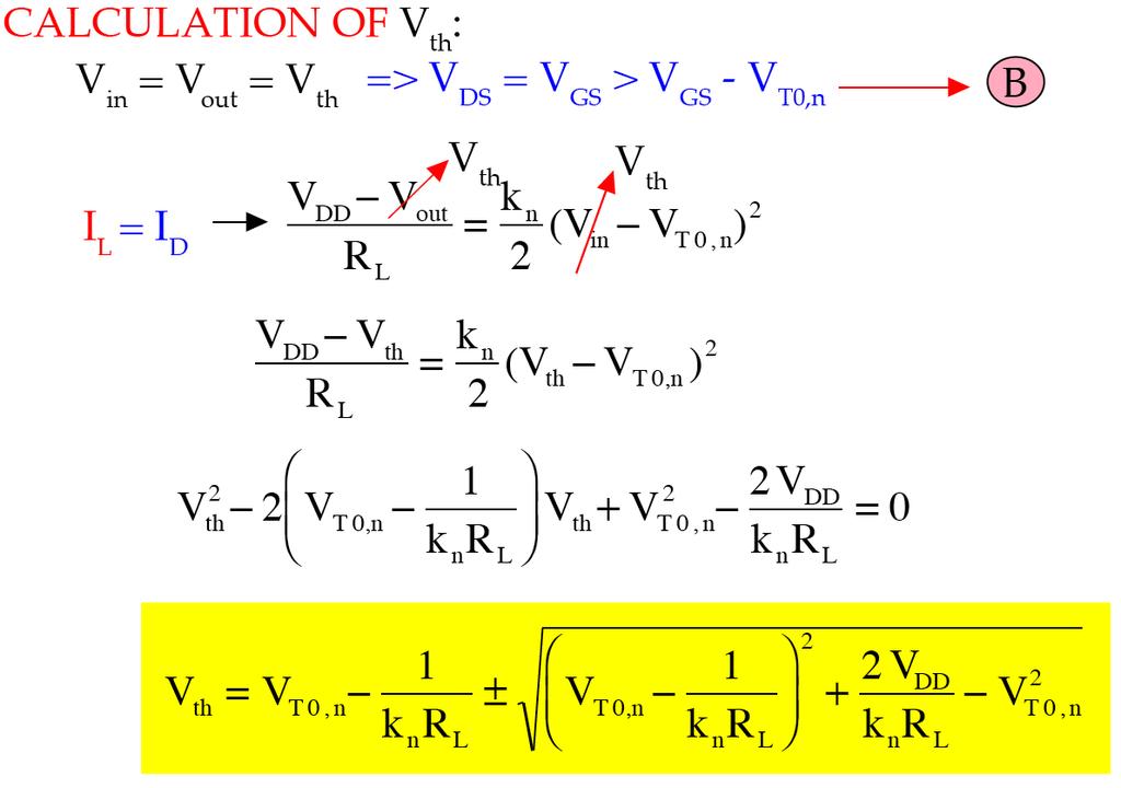
15 CALCULTION OF Vth 15
16 VDD 0 VT0n VDD 16
17 Take Limit as knrl -> -> VT0n -> VT0n V out.v in=v IL /=V DD -> VT0n 1 k n RL -> VDD - 2 V DD -> 0 V out.v in =V IH /= 3 k n RL -> 0 Vout VDD knrl -> semi-ideal VTC 0 VT0n VDD Vin 17
18 1 V DD P static.average/= [ I D.V in =0/* I D.V in =V DD /] 2 Vin = 0 P(Vin = 0 ) = 0 Vin = VDD Vout = VOL V DD V OL ID(Vin = 1 ) = IL = RL V DD V OL P(Vin = 1 ).=V DD RL Pstatic (average) 18
19 VDD Multiplying by RL 6 2.V V OL / W / DD 30 x 10 W 2 R = = 0 L 5 0.2= R [2.5 1/ / ' 2 6 ] 2 L L k n.2.v 2 DD VLT0n/V OL V OL / 30 x / / / W R L=2.05 x L NO UNIQUE W/L, RL 19
20 W 5 R L =2.05 x 10 0 L Pstatic (average) [mw] V DD V DD V OL P static.average /= 2 RL 20
21 VOL = V or V? 21

22 Preferred Design 22

23 SATURATED NMOS ENHANCEMENT-LOAD INVERTER VSB,L 0 VSB,d VSB,L 23

24 SATURATED NMOS ENHANCEMENT-LOAD INVERTER 24
25 NMOS DEPLETION-LOAD INVERTER ENH& DEP LOADS REPLACED BY CMOS! 25

26 QUICK REVIEW Visual Representation of the NMOS Resistive-Load Inverter driver transistor A ID = 0 C < B 26
27 QUICK REVIEW VDD 0 VT0n VDD 27
28 QUICK REVIEW W 5 R L =2.05 x 10 0 L Pstatic (average) [mw] V DD V DD V OL P static.average /= 2 RL 28
29 => VGSp = Vin - VDD => VDSp = Vout - VDD IDn = IDp 29
30 Visual Representation of the CMOS Inverter A Vout A E V OH =V DD -1 LIN LIN & OFF SAT V in+v T0n Vout = Vin - VT0n E SAT LIN LIN & V in,v DD *V T0p OFF -VT0p V OL=0 -VT0n Vout = Vin - VT0p -1 VT0n V IL V th V DD V IH VDD+VT0p Vin 30
31 Visual Representation of the CMOS Inverter Vout A E V OH =V DD -1 SAT & SAT -1 V th V IL SAT SAT -VT0p VT0n Vout = Vin - VT0n LIN LIN & SAT V OL=0 -VT0n Vout = Vin - VT0p LIN LIN & SAT V DD V IH VDD+VT0p Vin 31
 V in -1 -VT0n V th V IL V IH V DD")
32 IDn = IDp Vout = Vin - VT0p -1 Vout = Vin - VT0n V th V T0p V th V th V T0n V out = (iff λ = 0) V in -1 -VT0n V th V IL V IH V DD 32
33 IDn = IDp = 0 0= IDn = IDp = 0 =0 33
34 IDn = IDp Eq.(1) 34
 [ 2.V out V DD / ] d V in Eq.(2) SOLVE Eq. (1) and Eq.")
35 (1) Eq.(1) (and set Vin = VIL) ' n ' p (-1) VIL VIL k W k W d V out. / 2.V in V T0n /=. / [2.V out V DD /*2.V in V DD V T0p / ] 2 L n 2 L p d V in d V out (-1) [ 2.V out V DD / ] d V in Eq.(2) SOLVE Eq. (1) and Eq. (2) for Vout and VIL or use simulation. 35
36 IDn = IDp 36
 for Vout and VIH or use simulation.")
37 Eq.(3) Eq.(4) SOLVE Eq. (3) and Eq. (4) for Vout and VIH or use simulation. 37
38 IDn = IDp 38
 where k 'n.w / L/n 2n.W / L/n k R= ' = k p.")

39 Setting for Vin = Vth and solving for Vth Eq.(5) where k 'n.w / L/n 2n.W / L/n k R= ' = k p.w / L/ p 2 p.w / L/ p RECALL THAT 2n,2 p Usually Ln = Lp is set to min L: k 'n.w / L/n 2n W n k R= ' = k p.w / L/ p 2 p W p 39
40 DESIGN OF CMOS INVERTERS V T0n * V th = - 1.V DD *V T0p / kr - 1 1* kr Solving Eq.(5) for kr If Vth is Eq.(5) Eq.(5) V DD *V T0p V th k R =. / V th V T0n 2 Important design Eq. for CMOS inverter VTC. 1 ideal Vth set to V th =V th.ideal /= 2 V DD 0.5V DD *V T0p 2 2n.W / L/n k R=. /= 0.5 V DD V T0n 2 p.w / L/ p Symmetric CMOS Inverter W p 2n W n. /=. / V VT0n = -V = -VV =>=(k )symmetric =1.k=> / =1 If Vand and V = V If,th(ideal) also T0p T0 R R symetric th(ideal) T0n T0p T0 Lp 2 p Ln 40
41 Vth vs. 1/kR Vth (volts) 1 2p W p = k R 2n W n V th = where Ln = Lp 1/kR - 1 V T0n *.V DD *V T0p / kr 1* - 1 kr VDD = 5V; VT0n = - VT0p = 1 V 41
 and Eq. (2) FROM Eq. (3) and Eq.")
42 Symmetric CMOS inverter Vth(ideal) and VT0n = - VT0p = VT0 =>.k R /symetric =1.W / L/ p 2.52.W / L/n FROM Eq. (1) and Eq. (2) FROM Eq. (3) and Eq. (4) Symmetrical 42
, i.e. in IL 2 V 2IL 2V IL V T0 *V 2T0 1.=2 V 2IL 2V IL V DD *2 V IL V T0 V IL V DD *V 2DD V T0 V DD V 2IL *V IL V DD V 2DD 4 3 2 2 V IL V DD 4 V IL V T0 = V T0 V T0 V DD * V 2DD 4 3 V IL.")
43 DERIVE: for Symmetric CMOS Inverter Symmetric CMOS inverter: Vth = VDD/2, VT0n = - VT0p = VT0 and kr = 1 Eq.(1) Eq.(2) 1 => V IL =V out 2 V DD Substitute V out =V IL * 1 V DD, V = V and Sym-Inv Cond. into Eq.(1), i.e. in IL 2 V 2IL 2V IL V T0 *V 2T0 1.=2 V 2IL 2V IL V DD *2 V IL V T0 V IL V DD *V 2DD V T0 V DD V 2IL *V IL V DD V 2DD V IL V DD 4 V IL V T0 = V T0 V T0 V DD * V 2DD 4 3 V IL.2 V DD 4V T0 /= V 2DD V T0 V DD V 2T0 V = 1.3V DD *2V T0 /.V DD 2V T0 / QED IL 4 8 V 2V DD T0 43
 1. NMH, NML > VDD/4 = 1.25 V 2. Ideal NM => NMH = NML = 2.")
44 EXAMPLE: Compute the noise margins for a symmetric CMOS inverter has been designed to achieve Vth = VDD/2, where VDD = 5 V and VT0n = - VT0p = 1 V. V DD NM H =V OH V IH =V DD. V DD V T0 /= V DD * V T0 =2.125V NM L =V IL V OL=V IL = V DD * V T0 = V DD * V T0 =2.125V RECALL (with VDD = 5 V) 1. NMH, NML > VDD/4 = 1.25 V 2. Ideal NM => NMH = NML = 2.5 V > VDD/2 44
45 Pstatic Pstatic = 0 45

46 If the inverter cell is part of a standard cell library, it will adhere to the cell layout protocols. Smaller Area Layout 46
47 VDD Vout > - VT0p Pstatic > 0 47
4.10 The CMOS Digital Logic Inverter
 11/11/2004 section 4_10 The CMOS Digital Inverter blank.doc 1/1 4.10 The CMOS Digital Logic Inverter Reading Assignment: pp. 336346 Complementary MOSFET (CMOS) is the predominant technology for constructing
MOSFET and CMOS Gate. Copy Right by Wentai Liu
 MOSFET and CMOS Gate CMOS Inverter DC Analysis - Voltage Transfer Curve (VTC) Find (1) (2) (3) (4) (5) (6) V OH min, V V OL min, V V IH min, V V IL min, V OHmax OLmax IHmax ILmax NM L = V ILmax V OL max
CMOS Inverter (static view)
") Review: Design Abstraction Levels SYSTEM CMOS Inverter (static view) + MODULE GATE [Adapted from Chapter 5. 5.3 CIRCUIT of G DEVICE Rabaey s Digital Integrated Circuits,, J. Rabaey et al.] S D Review:
Review: Design Abstraction Levels SYSTEM CMOS Inverter (static view) + MODULE GATE [Adapted from Chapter 5. 5.3 CIRCUIT of G DEVICE Rabaey s Digital Integrated Circuits,, J. Rabaey et al.] S D Review:
Digital Integrated Circuits
 Chapter 6 The CMOS Inverter 1 Contents Introduction (MOST models) 0, 1 st, 2 nd order The CMOS inverter : The static behavior: o DC transfer characteristics, o Short-circuit current The CMOS inverter :
ECE 342 Solid State Devices & Circuits 4. CMOS
 ECE 34 Solid State Devices & Circuits 4. CMOS Jose E. Schutt-Aine Electrical & Computer Engineering University of Illinois jschutt@emlab.uiuc.edu ECE 34 Jose Schutt Aine 1 Digital Circuits V IH : Input
EEE 421 VLSI Circuits
 EEE 421 CMOS Properties Full rail-to-rail swing high noise margins» Logic levels not dependent upon the relative device sizes transistors can be minimum size ratioless Always a path to V dd or GND in steady
CMPEN 411 VLSI Digital Circuits. Lecture 04: CMOS Inverter (static view)
") CMPEN 411 VLSI Digital Circuits Lecture 04: CMOS Inverter (static view) Kyusun Choi [Adapted from Rabaey s Digital Integrated Circuits, Second Edition, 2003 J. Rabaey, A. Chandrakasan, B. Nikolic] CMPEN
CMPEN 411 VLSI Digital Circuits Lecture 04: CMOS Inverter (static view) Kyusun Choi [Adapted from Rabaey s Digital Integrated Circuits, Second Edition, 2003 J. Rabaey, A. Chandrakasan, B. Nikolic] CMPEN
THE INVERTER. Inverter
 THE INVERTER DIGITAL GATES Fundamental Parameters Functionality Reliability, Robustness Area Performance» Speed (delay)» Power Consumption» Energy Noise in Digital Integrated Circuits v(t) V DD i(t) (a)
CHAPTER 15 CMOS DIGITAL LOGIC CIRCUITS
 CHAPTER 5 CMOS DIGITAL LOGIC CIRCUITS Chapter Outline 5. CMOS Logic Gate Circuits 5. Digital Logic Inverters 5.3 The CMOS Inverter 5.4 Dynamic Operation of the CMOS Inverter 5.5 Transistor Sizing 5.6 Power
ESE 570: Digital Integrated Circuits and VLSI Fundamentals
 ESE 570: Digital Integrated Circuits and VLSI Fundamentals Lec 8: February 9, 016 MOS Inverter: Static Characteristics Lecture Outline! Voltage Transfer Characteristic (VTC) " Static Discipline Noise Margins!
EE115C Digital Electronic Circuits Homework #3
 Electrical Engineering Department Spring 1 EE115C Digital Electronic Circuits Homework #3 Due Thursday, April, 6pm @ 56-147E EIV Solution Problem 1 VTC and Inverter Analysis Figure 1a shows a standard
ENGR890 Digital VLSI Design Fall Lecture 4: CMOS Inverter (static view)
") ENGR89 Digital VLSI Design Fall 5 Lecture 4: CMOS Inverter (static view) [Adapted from Chapter 5 of Digital Integrated Circuits, 3, J. Rabaey et al.] [Also borrowed from Vijay Narayanan and Mary Jane Irwin]
ENGR89 Digital VLSI Design Fall 5 Lecture 4: CMOS Inverter (static view) [Adapted from Chapter 5 of Digital Integrated Circuits, 3, J. Rabaey et al.] [Also borrowed from Vijay Narayanan and Mary Jane Irwin]
Chapter 11. Inverter. DC AC, Switching. Layout. Sizing PASS GATES (CHPT 10) Other Inverters. Baker Ch. 11 The Inverter. Introduction to VLSI
 Other Inverters. Baker Ch. 11 The Inverter. Introduction to VLSI") Chapter 11 Inverter DC AC, Switching Ring Oscillator Dynamic Power Dissipation Layout LATCHUP Sizing PASS GATES (CHPT 10) Other Inverters Joseph A. Elias, Ph.D. Adjunct Professor, University of Kentucky;
Chapter 11 Inverter DC AC, Switching Ring Oscillator Dynamic Power Dissipation Layout LATCHUP Sizing PASS GATES (CHPT 10) Other Inverters Joseph A. Elias, Ph.D. Adjunct Professor, University of Kentucky;
Lecture 13 - Digital Circuits (II) MOS Inverter Circuits. March 20, 2003
 MOS Inverter Circuits. March 20, 2003") 6.012 Microelectronic Devices and Circuits Spring 2003 Lecture 131 Lecture 13 Digital Circuits (II) MOS Inverter Circuits March 20, 2003 Contents: 1. NMOS inverter with resistor pullup (cont.) 2. NMOS
6.012 Microelectronic Devices and Circuits Spring 2003 Lecture 131 Lecture 13 Digital Circuits (II) MOS Inverter Circuits March 20, 2003 Contents: 1. NMOS inverter with resistor pullup (cont.) 2. NMOS
EE5311- Digital IC Design
 EE5311- Digital IC Design Module 3 - The Inverter Janakiraman V Assistant Professor Department of Electrical Engineering Indian Institute of Technology Madras Chennai September 6, 2017 Janakiraman, IITM
ECE 342 Electronic Circuits. Lecture 35 CMOS Delay Model
 ECE 34 Electronic Circuits Lecture 35 CMOS Delay Model Jose E. Schutt-Aine Electrical & Computer Engineering University of Illinois jesa@illinois.edu ECE 34 Jose Schutt Aine 1 Digital Circuits V IH : Input
DC and Transient Responses (i.e. delay) (some comments on power too!)
 (some comments on power too!)") DC and Transient Responses (i.e. delay) (some comments on power too!) Michael Niemier (Some slides based on lecture notes by David Harris) 1 Lecture 02 - CMOS Transistor Theory & the Effects of Scaling
DC and Transient Responses (i.e. delay) (some comments on power too!) Michael Niemier (Some slides based on lecture notes by David Harris) 1 Lecture 02 - CMOS Transistor Theory & the Effects of Scaling
Lecture 12 Circuits numériques (II)
") Lecture 12 Circuits numériques (II) Circuits inverseurs MOS Outline NMOS inverter with resistor pull-up The inverter NMOS inverter with current-source pull-up Complementary MOS (CMOS) inverter Static analysis
Lecture 12 Circuits numériques (II) Circuits inverseurs MOS Outline NMOS inverter with resistor pull-up The inverter NMOS inverter with current-source pull-up Complementary MOS (CMOS) inverter Static analysis
CPE/EE 427, CPE 527 VLSI Design I L06: CMOS Inverter, CMOS Logic Gates. Course Administration. CMOS Inverter: A First Look
 CPE/EE 47, CPE 57 VLSI esign I L6: CMOS Inverter, CMOS Logic Gates epartment of Electrical and Computer Engineering University of labama in Huntsville leksandar Milenkovic ( www.ece.uah.edu/~milenka )
EE 434 Lecture 33. Logic Design
 EE 434 Lecture 33 Logic Design Review from last time: Ask the inverter how it will interpret logic levels V IN V OUT V H =? V L =? V LARGE V H V L V H Review from last time: The two-inverter loop X Y X
CMOS Inverter: CPE/EE 427, CPE 527 VLSI Design I L06: CMOS Inverter, CMOS Logic Gates. Course Administration. CMOS Properties.
 CMOS Inverter: Steady State Response CPE/EE 47, CPE 57 VLSI esign I L6: CMOS Inverter, CMOS Logic Gates R p V OL = V OH = V M = f(r n, R p ) epartment of Electrical and Computer Engineering University
EE5311- Digital IC Design
 EE5311- Digital IC Design Module 3 - The Inverter Janakiraman V Assistant Professor Department of Electrical Engineering Indian Institute of Technology Madras Chennai September 3, 2018 Janakiraman, IITM
Lecture 4: DC & Transient Response
 Introduction to CMOS VLSI Design Lecture 4: DC & Transient Response David Harris Harvey Mudd College Spring 004 Outline DC Response Logic Levels and Noise Margins Transient Response Delay Estimation Slide
Integrated Circuits & Systems
 Federal University of Santa Catarina Center for Technology Computer Science & Electronics Engineering Integrated Circuits & Systems INE 5442 Lecture 12 The CMOS Inverter: static behavior guntzel@inf.ufsc.br
Miscellaneous Lecture topics. Mary Jane Irwin [Adapted from Rabaey s Digital Integrated Circuits, 2002, J. Rabaey et al.]
![Miscellaneous Lecture topics. Mary Jane Irwin [Adapted from Rabaey s Digital Integrated Circuits, 2002, J. Rabaey et al.]](/thumbs/81/84503671.jpg "Miscellaneous Lecture topics. Mary Jane Irwin [Adapted from Rabaey s Digital Integrated Circuits, 2002, J. Rabaey et al.]") Miscellaneous Lecture topics Mary Jane Irwin [dapted from Rabaey s Digital Integrated Circuits, 2002, J. Rabaey et al.] MOS Switches MOS transistors can be viewed as simple switches. In an N-Switch, the
Miscellaneous Lecture topics Mary Jane Irwin [dapted from Rabaey s Digital Integrated Circuits, 2002, J. Rabaey et al.] MOS Switches MOS transistors can be viewed as simple switches. In an N-Switch, the
ECE 438: Digital Integrated Circuits Assignment #4 Solution The Inverter
 ECE 438: Digital Integrated Circuits Assignment #4 The Inverter Text: Chapter 5, Digital Integrated Circuits 2 nd Ed, Rabaey 1) Consider the CMOS inverter circuit in Figure P1 with the following parameters.
2007 Fall: Electronic Circuits 2 CHAPTER 10. Deog-Kyoon Jeong School of Electrical Engineering
 007 Fall: Electronic Circuits CHAPTER 10 Digital CMOS Logic Circuits Deog-Kyoon Jeong dkjeong@snu.ac.kr k School of Electrical Engineering Seoul lnational luniversity it Introduction In this chapter, we
Lecture 11 VTCs and Delay. No lab today, Mon., Tues. Labs restart next week. Midterm #1 Tues. Oct. 7 th, 6:30-8:00pm in 105 Northgate
 EE4-Fall 2008 Digital Integrated Circuits Lecture VTCs and Delay Lecture # Announcements No lab today, Mon., Tues. Labs restart next week Midterm # Tues. Oct. 7 th, 6:30-8:00pm in 05 Northgate Exam is
EE 330 Lecture 37. Digital Circuits. Other Logic Families. Propagation Delay basic characterization Device Sizing (Inverter and multiple-input gates)
") EE 330 Lecture 37 Digital Circuits Other Logic Families Static Power Dissipation Propagation Delay basic characterization Device Sizing (Inverter and multiple-input gates) Review from Last Time Inverter
EE 330 Lecture 37 Digital Circuits Other Logic Families Static Power Dissipation Propagation Delay basic characterization Device Sizing (Inverter and multiple-input gates) Review from Last Time Inverter
Integrated Circuit Design ELCT 701 (Winter 2017) Lecture 2: Resistive Load Inverter
 Lecture 2: Resistive Load Inverter") 1 Integrated Circuit Design ELCT 701 (Winter 017) Lecture : Resistive Load Inverter Assistant Professor Office: C3.315 E-mail: eman.azab@guc.edu.eg Digital Inverters Introduction 3 Digital Inverter: Introduction
1 Integrated Circuit Design ELCT 701 (Winter 017) Lecture : Resistive Load Inverter Assistant Professor Office: C3.315 E-mail: eman.azab@guc.edu.eg Digital Inverters Introduction 3 Digital Inverter: Introduction
EE5780 Advanced VLSI CAD
 EE5780 Advanced VLSI CAD Lecture 4 DC and Transient Responses, Circuit Delays Zhuo Feng 4.1 Outline Pass Transistors DC Response Logic Levels and Noise Margins Transient Response RC Delay Models Delay
ECE 546 Lecture 10 MOS Transistors
 ECE 546 Lecture 10 MOS Transistors Spring 2018 Jose E. Schutt-Aine Electrical & Computer Engineering University of Illinois jesa@illinois.edu NMOS Transistor NMOS Transistor N-Channel MOSFET Built on p-type
5.0 CMOS Inverter. W.Kucewicz VLSICirciuit Design 1
 5.0 CMOS Inverter W.Kucewicz VLSICirciuit Design 1 Properties Switching Threshold Dynamic Behaviour Capacitance Propagation Delay nmos/pmos Ratio Power Consumption Contents W.Kucewicz VLSICirciuit Design
Fig. 1 CMOS Transistor Circuits (a) Inverter Out = NOT In, (b) NOR-gate C = NOT (A or B)
 Inverter Out = NOT In, (b) NOR-gate C = NOT (A or B)") 1 Introduction to Transistor-Level Logic Circuits 1 By Prawat Nagvajara At the transistor level of logic circuits, transistors operate as switches with the logic variables controlling the open or closed
1 Introduction to Transistor-Level Logic Circuits 1 By Prawat Nagvajara At the transistor level of logic circuits, transistors operate as switches with the logic variables controlling the open or closed
EEC 116 Lecture #5: CMOS Logic. Rajeevan Amirtharajah Bevan Baas University of California, Davis Jeff Parkhurst Intel Corporation
 EEC 116 Lecture #5: CMOS Logic Rajeevan mirtharajah Bevan Baas University of California, Davis Jeff Parkhurst Intel Corporation nnouncements Quiz 1 today! Lab 2 reports due this week Lab 3 this week HW
Midterm. ESE 570: Digital Integrated Circuits and VLSI Fundamentals. Lecture Outline. Pass Transistor Logic. Restore Output.
 ESE 570: Digital Integrated Circuits and VLSI Fundamentals Lec 16: March 21, 2017 Transmission Gates, Euler Paths, Energy Basics Review Midterm! Midterm " Mean: 79.5 " Standard Dev: 14.5 2 Lecture Outline!
VLSI Design and Simulation
 VLSI Design and Simulation CMOS Inverters Topics Inverter VTC Noise Margin Static Load Inverters CMOS Inverter First-Order DC Analysis R p V OL = 0 V OH = R n =0 = CMOS Inverter: Transient Response R p
Lecture 5: DC & Transient Response
 Lecture 5: DC & Transient Response Outline q Pass Transistors q DC Response q Logic Levels and Noise Margins q Transient Response q RC Delay Models q Delay Estimation 2 Activity 1) If the width of a transistor
ECE321 Electronics I
 ECE31 Electronics Lecture 1: CMOS nverter: Noise Margin & Delay Model Payman Zarkesh-Ha Office: ECE Bldg. 30B Office hours: Tuesday :00-3:00PM or by appointment E-mail: payman@ece.unm.edu Slide: 1 CMOS
ESE 570: Digital Integrated Circuits and VLSI Fundamentals
 ESE 570: Digital Integrated Circuits and VLSI Fundamentals Lec 15: March 15, 2018 Euler Paths, Energy Basics and Optimization Midterm! Midterm " Mean: 89.7 " Standard Dev: 8.12 2 Lecture Outline! Euler
The CMOS Inverter: A First Glance
 The CMOS Inverter: A First Glance V DD S D V in V out C L D S CMOS Inverter N Well V DD V DD PMOS 2λ PMOS Contacts In Out In Out Metal 1 NMOS Polysilicon NMOS GND CMOS Inverter: Steady State Response V
VLSI Design Issues. ECE 410, Prof. F. Salem/Prof. A. Mason notes update
 VLSI Design Issues Scaling/Moore s Law has limits due to the hysics of material. Now L (L=20nm??) affects tx delays (seed), noise, heat (ower consumtion) Scaling increases density of txs and requires more
Lecture 12 Digital Circuits (II) MOS INVERTER CIRCUITS
 MOS INVERTER CIRCUITS") Lecture 12 Digital Circuits (II) MOS INVERTER CIRCUITS Outline NMOS inverter with resistor pull-up The inverter NMOS inverter with current-source pull-up Complementary MOS (CMOS) inverter Static analysis
Lecture 12 Digital Circuits (II) MOS INVERTER CIRCUITS Outline NMOS inverter with resistor pull-up The inverter NMOS inverter with current-source pull-up Complementary MOS (CMOS) inverter Static analysis
EEC 118 Lecture #5: CMOS Inverter AC Characteristics. Rajeevan Amirtharajah University of California, Davis Jeff Parkhurst Intel Corporation
 EEC 8 Lecture #5: CMOS Inverter AC Characteristics Rajeevan Amirtharajah University of California, Davis Jeff Parkhurst Intel Corporation Acknowledgments Slides due to Rajit Manohar from ECE 547 Advanced
EEC 118 Lecture #6: CMOS Logic. Rajeevan Amirtharajah University of California, Davis Jeff Parkhurst Intel Corporation
 EEC 118 Lecture #6: CMOS Logic Rajeevan mirtharajah University of California, Davis Jeff Parkhurst Intel Corporation nnouncements Quiz 1 today! Lab 2 reports due this week Lab 3 this week HW 3 due this
5. CMOS Gate Characteristics CS755
 5. CMOS Gate Characteristics Last module: CMOS Transistor theory This module: DC Response Logic Levels and Noise Margins Transient Response Delay Estimation Transistor ehavior 1) If the width of a transistor
ECE 342 Electronic Circuits. 3. MOS Transistors
 ECE 342 Electronic Circuits 3. MOS Transistors Jose E. Schutt-Aine Electrical & Computer Engineering University of Illinois jschutt@emlab.uiuc.edu 1 NMOS Transistor Typically L = 0.1 to 3 m, W = 0.2 to
Topic 4. The CMOS Inverter
 Topic 4 The CMOS Inverter Peter Cheung Department of Electrical & Electronic Engineering Imperial College London URL: www.ee.ic.ac.uk/pcheung/ E-mail: p.cheung@ic.ac.uk Topic 4-1 Noise in Digital Integrated
Lecture 310 Open-Loop Comparators (3/28/10) Page 310-1
 Page 310-1") Lecture 310 Open-Loop Comparators (3/28/10) Page 310-1 LECTURE 310 OPEN-LOOP COMPARATORS LECTURE ORGANIZATION Outline Characterization of comparators Dominant pole, open-loop comparators Two-pole, open-loop
Lecture 310 Open-Loop Comparators (3/28/10) Page 310-1 LECTURE 310 OPEN-LOOP COMPARATORS LECTURE ORGANIZATION Outline Characterization of comparators Dominant pole, open-loop comparators Two-pole, open-loop
L ECE 4211 UConn F. Jain Scaling Laws for NanoFETs Chapter 10 Logic Gate Scaling
 L13 04202017 ECE 4211 UConn F. Jain Scaling Laws for NanoFETs Chapter 10 Logic Gate Scaling Scaling laws: Generalized scaling (GS) p. 610 Design steps p.613 Nanotransistor issues (page 626) Degradation
Digital Microelectronic Circuits ( ) The CMOS Inverter. Lecture 4: Presented by: Adam Teman
 The CMOS Inverter. Lecture 4: Presented by: Adam Teman") Digital Microelectronic Circuits (361-1-301 ) Presented by: Adam Teman Lecture 4: The CMOS Inverter 1 Last Lectures Moore s Law Terminology» Static Properties» Dynamic Properties» Power The MOSFET Transistor»
Digital Microelectronic Circuits (361-1-301 ) Presented by: Adam Teman Lecture 4: The CMOS Inverter 1 Last Lectures Moore s Law Terminology» Static Properties» Dynamic Properties» Power The MOSFET Transistor»
VLSI Design I; A. Milenkovic 1
 ourse dministration PE/EE 47, PE 57 VLI esign I L6: tatic MO Logic epartment of Electrical and omputer Engineering University of labama in Huntsville leksandar Milenkovic ( www. ece.uah.edu/~milenka )
CMOS INVERTER. Last Lecture. Metrics for qualifying digital circuits. »Cost» Reliability» Speed (delay)»performance
»performance") CMOS INVERTER Last Lecture Metrics for qualifying digital circuits»cost» Reliability» Speed (delay)»performance 1 Today s lecture The CMOS inverter at a glance An MOS transistor model for manual analysis
CMOS INVERTER Last Lecture Metrics for qualifying digital circuits»cost» Reliability» Speed (delay)»performance 1 Today s lecture The CMOS inverter at a glance An MOS transistor model for manual analysis
EECS 141: FALL 05 MIDTERM 1
 University of California College of Engineering Department of Electrical Engineering and Computer Sciences D. Markovic TuTh 11-1:3 Thursday, October 6, 6:3-8:pm EECS 141: FALL 5 MIDTERM 1 NAME Last SOLUTION
MOS Transistor Theory
 CHAPTER 3 MOS Transistor Theory Outline 2 1. Introduction 2. Ideal I-V Characteristics 3. Nonideal I-V Effects 4. C-V Characteristics 5. DC Transfer Characteristics 6. Switch-level RC Delay Models MOS
VLSI Design I; A. Milenkovic 1
 PE/EE 47, PE 57 VLI esign I L6: tatic MO Logic epartment of Electrical and omputer Engineering University of labama in Huntsville leksandar Milenkovic ( www. ece.uah.edu/~milenka ) www. ece.uah.edu/~milenka/cpe57-3f
Lecture Outline. ESE 570: Digital Integrated Circuits and VLSI Fundamentals. Review: 1st Order RC Delay Models. Review: Two-Input NOR Gate (NOR2)
") ESE 570: Digital Integrated Circuits and VLSI Fundamentals Lec 14: March 1, 2016 Combination Logic: Ratioed and Pass Logic Lecture Outline! CMOS Gates Review " CMOS Worst Case Analysis! Ratioed Logic Gates!
ESE 570: Digital Integrated Circuits and VLSI Fundamentals Lec 14: March 1, 2016 Combination Logic: Ratioed and Pass Logic Lecture Outline! CMOS Gates Review " CMOS Worst Case Analysis! Ratioed Logic Gates!
Power Consumption in CMOS CONCORDIA VLSI DESIGN LAB
 Power Consumption in CMOS 1 Power Dissipation in CMOS Two Components contribute to the power dissipation:» Static Power Dissipation Leakage current Sub-threshold current» Dynamic Power Dissipation Short
Lecture 4: CMOS review & Dynamic Logic
 Lecture 4: CMOS review & Dynamic Logic Reading: ch5, ch6 Overview CMOS basics Power and energy in CMOS Dynamic logic 1 CMOS Properties Full rail-to-rail swing high noise margins Logic levels not dependent
The CMOS Inverter: A First Glance
 The CMOS Inverter: A First Glance V DD V in V out C L CMOS Properties Full rail-to-rail swing Symmetrical VTC Propagation delay function of load capacitance and resistance of transistors No static power
Lecture 6: DC & Transient Response
 Lecture 6: DC & Transient Response Slides courtesy of Deming Chen Slides based on the initial set from David Harris CMOS VLSI Design Outline Pass Transistors DC Response Logic Levels and Noise Margins
DC and Transient. Courtesy of Dr. Daehyun Dr. Dr. Shmuel and Dr.
 DC and Transient Courtesy of Dr. Daehyun Lim@WSU, Dr. Harris@HMC, Dr. Shmuel Wimer@BIU and Dr. Choi@PSU http://csce.uark.edu +1 (479) 575-604 yrpeng@uark.edu Pass Transistors We have assumed source is
Properties of CMOS Gates Snapshot
 MOS logic 1 Properties of MOS Gates Snapshot High noise margins: V OH and V OL are at V DD and GND, respectively. No static power consumption: There never exists a direct path between V DD and V SS (GND)
VLSI Design I; A. Milenkovic 1
 ourse dministration PE/EE 47, PE 57 VLI esign I L6: omplementary MO Logic Gates epartment of Electrical and omputer Engineering University of labama in Huntsville leksandar Milenkovic ( www.ece.uah.edu/~milenka
Homework Assignment #3 EE 477 Spring 2017 Professor Parker , -.. = 1.8 -, 345 = 0 -
 Homework Assignment #3 EE 477 Spring 2017 Professor Parker Note:! " = $ " % &' ( ) * ),! + = $ + % &' (, *,, -.. = 1.8 -, 345 = 0 - Question 1: a) (8%) Define the terms V OHmin, V IHmin, V ILmax and V
COMBINATIONAL LOGIC. Combinational Logic
 COMINTIONL LOGIC Overview Static CMOS Conventional Static CMOS Logic Ratioed Logic Pass Transistor/Transmission Gate Logic Dynamic CMOS Logic Domino np-cmos Combinational vs. Sequential Logic In Logic
Lecture 14 - Digital Circuits (III) CMOS. April 1, 2003
 CMOS. April 1, 2003") 6.12 - Microelectronic Devices and Circuits - Spring 23 Lecture 14-1 Lecture 14 - Digital Circuits (III) CMOS April 1, 23 Contents: 1. Complementary MOS (CMOS) inverter: introduction 2. CMOS inverter:
6.12 - Microelectronic Devices and Circuits - Spring 23 Lecture 14-1 Lecture 14 - Digital Circuits (III) CMOS April 1, 23 Contents: 1. Complementary MOS (CMOS) inverter: introduction 2. CMOS inverter:
Lecture 5: DC & Transient Response
 Lecture 5: DC & Transient Response Outline Pass Transistors DC Response Logic Levels and Noise Margins Transient Response RC Delay Models Delay Estimation 2 Pass Transistors We have assumed source is grounded
EE141Microelettronica. CMOS Logic
 Microelettronica CMOS Logic CMOS logic Power consumption in CMOS logic gates Where Does Power Go in CMOS? Dynamic Power Consumption Charging and Discharging Capacitors Short Circuit Currents Short Circuit
9/18/2008 GMU, ECE 680 Physical VLSI Design
 ECE680: Physical VLSI Design Chapter III CMOS Device, Inverter, Combinational circuit Logic and Layout Part 3 Combinational Logic Gates (textbook chapter 6) 9/18/2008 GMU, ECE 680 Physical VLSI Design
DC & Transient Responses
 ECEN454 Digital Integrated Circuit Design DC & Transient Responses ECEN 454 DC Response DC Response: vs. for a gate Ex: Inverter When = -> = When = -> = In between, depends on transistor size and current
CPE/EE 427, CPE 527 VLSI Design I Delay Estimation. Department of Electrical and Computer Engineering University of Alabama in Huntsville
 CPE/EE 47, CPE 57 VLSI Design I Delay Estimation Department of Electrical and Computer Engineering University of labama in Huntsville leksandar Milenkovic ( www.ece.uah.edu/~milenka ) Review: CMOS Circuit
ESE 570: Digital Integrated Circuits and VLSI Fundamentals
 ESE 570: Digital Integrated Circuits and VLSI Fundamentals Lec 10: February 16, 2016 MOS Inverter: Dynamic Characteristics Lecture Outline! Review: Symmetric CMOS Inverter Design! Inverter Power! Dynamic
ESE 570: Digital Integrated Circuits and VLSI Fundamentals
 ESE 570: Digital Integrated Circuits and VLSI Fundamentals Lec 10: February 15, 2018 MOS Inverter: Dynamic Characteristics Penn ESE 570 Spring 2018 Khanna Lecture Outline! Inverter Power! Dynamic Characteristics
P-MOS Device and CMOS Inverters
 Lecture 23 P-MOS Device and CMOS Inverters A) P-MOS Device Structure and Oeration B) Relation of Current to t OX, µ V LIMIT C) CMOS Device Equations and Use D) CMOS Inverter V OUT vs. V IN E) CMOS Short
MOS Transistor Theory
 MOS Transistor Theory So far, we have viewed a MOS transistor as an ideal switch (digital operation) Reality: less than ideal EE 261 Krish Chakrabarty 1 Introduction So far, we have treated transistors
Chapter 2 CMOS Transistor Theory. Jin-Fu Li Department of Electrical Engineering National Central University Jungli, Taiwan
 Chapter 2 CMOS Transistor Theory Jin-Fu Li Department of Electrical Engineering National Central University Jungli, Taiwan Outline Introduction MOS Device Design Equation Pass Transistor Jin-Fu Li, EE,
Digital Integrated Circuits 2nd Inverter
 Digital Integrated Circuits The Inverter The CMOS Inverter V DD Analysis Inverter complex gate Cost V in V out complexity & Area Integrity and robustness C L Static behavior Performance Dynamic response
EE115C Digital Electronic Circuits Homework #4
 EE115 Digital Electronic ircuits Homework #4 Problem 1 Power Dissipation Solution Vdd =1.0V onsider the source follower circuit used to drive a load L =20fF shown above. M1 and M2 are both NMOS transistors
The Physical Structure (NMOS)
") The Physical Structure (NMOS) Al SiO2 Field Oxide Gate oxide S n+ Polysilicon Gate Al SiO2 SiO2 D n+ L channel P Substrate Field Oxide contact Metal (S) n+ (G) L W n+ (D) Poly 1 Transistor Resistance Two
The Physical Structure (NMOS) Al SiO2 Field Oxide Gate oxide S n+ Polysilicon Gate Al SiO2 SiO2 D n+ L channel P Substrate Field Oxide contact Metal (S) n+ (G) L W n+ (D) Poly 1 Transistor Resistance Two
EE105 Fall 2014 Microelectronic Devices and Circuits. NMOS Transistor Capacitances: Saturation Region
 EE105 Fall 014 Microelectronic Devices and Circuits Prof. Ming C. Wu wu@eecs.berkeley.edu 511 Sutardja Dai Hall (SDH) 1 NMOS Transistor Capacitances: Saturation Region Drain no longer connected to channel
CMOS Logic Gates. University of Connecticut 181
 CMOS Logic Gates University of Connecticut 181 Basic CMOS Inverter Operation V IN P O N O p-channel enhancementtype MOSFET; V T < 0 n-channel enhancementtype MOSFET; V T > 0 If V IN 0, N O is cut off and
Lecture Outline. ESE 570: Digital Integrated Circuits and VLSI Fundamentals. Review: CMOS Inverter: Visual VTC. Review: CMOS Inverter: Visual VTC
 ESE 570: Digital Integrated Circuits and LSI Fundamentals Lec 0: February 4, 207 MOS Inverter: Dynamic Characteristics Lecture Outline! Review: Symmetric CMOS Inverter Design! Inverter Power! Dynamic Characteristics
EE 560 MOS INVERTERS: STATIC CHARACTERISTICS. Kenneth R. Laker, University of Pennsylvania
 1 EE 560 MOS INVETES: STTIC CHCTEISTICS Kenneth. aker, University of Pennsylvania IDE INVETE VOTGE TNSFE CHTEISTIC (VTC) B = 0 1 B 1 0 ogic 1 output ogic 0 output / Kenneth. aker, University of Pennsylvania
Today s lecture. EE141- Spring 2003 Lecture 4. Design Rules CMOS Inverter MOS Transistor Model
 - Spring 003 Lecture 4 Design Rules CMOS Inverter MOS Transistor Model Today s lecture Design Rules The CMOS inverter at a glance An MOS transistor model for manual analysis Important! Labs start next
Digital Microelectronic Circuits ( ) Ratioed Logic. Lecture 8: Presented by: Mr. Adam Teman
 Ratioed Logic. Lecture 8: Presented by: Mr. Adam Teman") Digital Microelectronic ircuits (361-1-3021 ) Presented by: Mr. Adam Teman Lecture 8: atioed Logic 1 Motivation In the previous lecture, we learned about Standard MOS Digital Logic design. MOS is unquestionably
Digital Microelectronic ircuits (361-1-3021 ) Presented by: Mr. Adam Teman Lecture 8: atioed Logic 1 Motivation In the previous lecture, we learned about Standard MOS Digital Logic design. MOS is unquestionably
ECE 6412, Spring Final Exam Page 1
 ECE 64, Spring 005 Final Exam Page FINAL EXAMINATION SOLUTIONS (Average score = 89/00) Problem (0 points This problem is required) A comparator consists of an amplifier cascaded with a latch as shown below.
Circuit A. Circuit B
 UNIVERSITY OF CALIFORNIA College of Engineering Department of Electrical Engineering and Computer Sciences Last modified on November 19, 2006 by Karl Skucha (kskucha@eecs) Borivoje Nikolić Homework #9
Review of Band Energy Diagrams MIS & MOS Capacitor MOS TRANSISTORS MOSFET Capacitances MOSFET Static Model
 Content- MOS Devices and Switching Circuits Review of Band Energy Diagrams MIS & MOS Capacitor MOS TRANSISTORS MOSFET Capacitances MOSFET Static Model A Cantoni 2009-2013 Digital Switching 1 Content- MOS
Name: Answers. Grade: Q1 Q2 Q3 Q4 Q5 Total. ESE370 Fall 2015
 University of Pennsylvania Department of Electrical and System Engineering Circuit-Level Modeling, Design, and Optimization for Digital Systems ESE370, Fall 2015 Midterm 1 Monday, September 28 5 problems
1/13/12 V DS. I d V GS. C ox ( = f (V GS ,V DS ,V SB = I D. + i d + I ΔV + I ΔV BS V BS. 19 January 2012
 /3/ 9 January 0 Study the linear model of MOS transistor around an operating point." MOS in saturation: V GS >V th and V S >V GS -V th " VGS vi - I d = I i d VS I d = µ n ( L V V γ Φ V Φ GS th0 F SB F
Chapter 5. The Inverter. V1. April 10, 03 V1.1 April 25, 03 V2.1 Nov Inverter
 Chapter 5 The Inverter V1. April 10, 03 V1.1 April 25, 03 V2.1 Nov.12 03 Objective of This Chapter Use Inverter to know basic CMOS Circuits Operations Watch for performance Index such as Speed (Delay calculation)
CHAPTER 5 MOS FIELD-EFFECT TRANSISTORS
 CHAPTER 5 MOS FIELD-EFFECT TRANSISTORS 5.1 The MOS capacitor 5.2 The enhancement-type N-MOS transistor 5.3 I-V characteristics of enhancement mode MOSFETS 5.4 The PMOS transistor and CMOS technology 5.5
SRAM Cell, Noise Margin, and Noise
 SRAM Cell, Noise Margin, and Noise C.K. Ken Yang UCLA yangck@ucla.edu Courtesy of MAH and BAW 1 Overview Reading Rabaey 5.3 W&H 2.5 Background Reading a memory cell can disturb its value. In addition,
Lecture 13 MOSFET as an amplifier with an introduction to MOSFET small-signal model and small-signal schematics. Lena Peterson
 Lecture 13 MOSFET as an amplifier with an introduction to MOSFET small-signal model and small-signal schematics Lena Peterson 2015-10-13 Outline (1) Why is the CMOS inverter gain not infinite? Large-signal
CMOS Logic Gates. University of Connecticut 172
 CMOS Logic Gates University of Connecticut 172 Basic CMOS Inverter Operation V IN P O N O p-channel enhancementtype MOSFET; V T < 0 n-channel enhancementtype MOSFET; V T > 0 If V IN 0, N O is cut off and
PASS-TRANSISTOR LOGIC. INEL Fall 2014
 PASS-TRANSISTOR LOGIC INEL 4207 - Fall 2014 Figure 15.5 Conceptual pass-transistor logic gates. (a) Two switches, controlled by the input variables B and C, when connected in series in the path between
ESE 570 MOS INVERTERS DYNAMIC CHARACTERISTICS. Kenneth R. Laker, University of Pennsylvania, updated 26Feb15
 ESE 570 MOS INVERTERS DYNAMIC CHARACTERISTICS 1 Usually Cdb >> Cgd & Csb >> Cgs extrinsic parasitic caps n = fan-out 1 # dbn Cload = C + #C# dbp +#C# gdn +#C# gdp +# C # int + ncgb Parasitic Caps updated
[ ] [ ] Chapter 16 Problem Solutions (a) = = = = Then 8 = 2(0.343) + V 2(0.343)
![[ ] [ ] Chapter 16 Problem Solutions (a) = = = = Then 8 = 2(0.343) + V 2(0.343)](/thumbs/80/81150009.jpg "[ ] [ ] Chapter 16 Problem Solutions (a) = = = = Then 8 = 2(0.343) + V 2(0.343)") Chater 6 Problem Solutions 6. (a) e N Δ V φ + V φ s a TN f SB f C ax 4 ax (3.9)(8.85 ) 8 ax 7.67 8 tax 45 / 9 4 5 8 e s Na.6.7 8.85 8 5.5 C Then 8 5.5 Δ VTN (.343) + V (.343) 8 SB 7.67 For V V : SB Δ VTN.67.686.686
Chater 6 Problem Solutions 6. (a) e N Δ V φ + V φ s a TN f SB f C ax 4 ax (3.9)(8.85 ) 8 ax 7.67 8 tax 45 / 9 4 5 8 e s Na.6.7 8.85 8 5.5 C Then 8 5.5 Δ VTN (.343) + V (.343) 8 SB 7.67 For V V : SB Δ VTN.67.686.686
ECE 6412, Spring Final Exam Page 1 FINAL EXAMINATION NAME SCORE /120
 ECE 6412, Spring 2002 Final Exam Page 1 FINAL EXAMINATION NAME SCORE /120 Problem 1O 2O 3 4 5 6 7 8 Score INSTRUCTIONS: This exam is closed book with four sheets of notes permitted. The exam consists of