Digital Fundamentals
|
|
|
- Scot Hunter
- 5 years ago
- Views:
Transcription


1 Digital Fundamentals Tenth Edition Floyd hapter 8 Modified by Yuttapong Jiraraksopakun Floyd, Digital Fundamentals, 10 th 2008 Pearson Education ENE, KMUTT ed 2009
2 ounting in Binary As you know, the binary count sequence follows a familiar pattern of 0 s and 1 s as described in Section 2-2 of the text. The next bit changes on every fourth number. Summary LSB changes on every number. The next bit changes on every other number.
3 ounting in Binary A counter can form the same pattern of 0 s and 1 s with logic levels. The first stage in the counter represents the least significant bit notice that these waveforms follow the same pattern as counting in binary. LSB MSB
4 Three bit Asynchronous ounter In an asynchronous counter, the clock is applied only to the first stage. Subsequent stages derive the clock from the previous stage. The three-bit asynchronous counter shown is typical. It uses J-K flip-flops in the toggle mode. HIGH J 0 J Q 1 1 J 2 LK K 0 Q 1 K 1 K 2 Waveforms are on the following slide
5 Three bit Asynchronous ounter Notice that the output is triggered on the leading edge of the clock signal. The following stage is triggered from. The leading edge of is equivalent to the trailing edge of. The resulting sequence is that of an 3-bit binary up counter. LK Q
6 Propagation Delay Summary Asynchronous counters are sometimes called ripple counters, because the stages do not all change together. For certain applications requiring high clock rates, this is a major disadvantage. Notice how delays are cumulative as each stage in a counter is clocked later than the previous stage. LK Q is delayed by 1 propagation delay, Q 1 by 2 delays and by 3 delays.
7 Asynchronous Decade ounter This counter uses partial decoding to recycle the count sequence to zero after the 1001 state. The flip-flops are trailing-edge triggered, so clocks are derived from the Q outputs. Other truncated sequences can be obtained using a similar technique. HIGH LR J 0 Q 1 J 1 J 2 J 3 Q 3 LK K 0 K 1 K 2 K 3 Waveforms are on the following slide
8 Asynchronous Decade ounter When Q 1 and Q 3 are HIGH together, the counter is cleared by a glitch on the LR line. LK Q 1 Glitch Glitch Q 3 LR Glitch

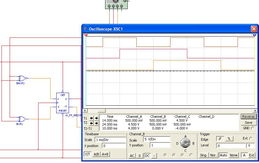
9 Asynchronous ounter Using D Flip-flops D flip-flops can be set to toggle and used as asynchronous counters by connecting Q back to D. The counter in this slide is a Multisim simulation of one described in the lab manual. an you figure out the sequence? LSB MSB Q to D puts D flip-flop in toggle mode The next slide shows the scope

10 LK LSB MSB LR Note that it is momentarily in state 3 which causes it to clear. The sequence is (LR) (repeat)
11 The 74LS93A Asynchronous ounter The 74LS93A has one independent toggle J-K flip-flop driven by LK A and three toggle J-K flip-flops that form an asynchronous counter driven by LK B. The counter can be extended to form a 4-bit counter by connecting to the LK B input. Two inputs are provided that clear the count. LK B (1) LK A (14) J J 1 J 2 0 J 3 K 0 K 1 K 2 K 3 All J and K inputs are connected internally HIGH RO (1) RO (2) (2) (3) (12) (9) (8) (11) Q 1 Q 3

12 The 74LS93A Asynchronous ounter

13 Synchronous ounters Summary In a synchronous counter all flip-flops are clocked together with a common clock pulse. Synchronous counters overcome the disadvantage of accumulated propagation delays, but generally they require more circuitry to control states changes.
14 Synchronous ounters Summary This 3-bit binary synchronous counter has the same count sequence as the 3-bit asynchronous counter shown previously. LK HIGH J J 1 J 0 2 K 0 Q 1 Q 1 K 1 K 2 The next slide shows how to analyze this counter by writing the logic equations for each input. Notice the inputs to each flip-flop
15 Analysis of Synchronous ounters A tabular technique for analysis is illustrated for the counter on the previous slide. Start by setting up the outputs as shown, then write the logic equation for each input. This has been done for the counter. 1. Put the counter in an arbitrary state; then determine the inputs for this state. Outputs 2. Use the new inputs to determine the next state: and Q 1 will latch and will toggle. Logic for inputs 3. Set up the next group of inputs from the current output. Q 1 J 2 = Q 1 K 2 = Q 1 J 1 = K 1 = J 0 = 1 K 0 = will latch again but both Q 1 and will toggle. ontinue like this, to complete the table. The next slide shows the completed table
16 Analysis of Synchronous ounters Outputs Logic for inputs Q 1 J 2 = Q 1 K 2 = Q 1 J 1 = K 1 = J 0 = 1 K 0 = At this points all states have been accounted for and the counter is ready to recycle
17 A 4-bit Synchronous Binary ounter Q 1 Q 1 FF0 FF1 G1 G 2 FF2 FF3 HIGH J 0 J 1 Q 1 J 2 J 3 Q 3 LK K 0 K 1 Q 1 K 2 K 3 Q 3 The 4-bit binary counter has one more AND gate than the 3-bit counter just described. The shaded areas show where the AND gate outputs are HIGH causing the next FF to toggle. Q 1 Q 3
18 BD Decade ounter With some additional logic, a binary counter can be converted to a BD synchronous decade counter. After reaching the count 1001, the counter recycles to HIGH Summary This gate detects 1001, and causes FF3 to toggle on the next clock pulse. FF0 toggles on every clock pulse. Thus, the count starts over at FF0 FF1 FF2 FF3 Q 3 J 0 J 1 Q 1 J 2 J 3 Q 3 K 0 K 1 Q 1 K 2 K 3 Q 3 Q 3 LK

19 BD Decade ounter Summary FF1 (Q1) toggle on the next clock pulse only if Q0 = 1 and Q3 = 0 HIGH FF0 FF1 FF2 FF3 J 0 _ Q 3 J 1 Q 1 J 2 J 3 Q 3 K 0 K 1 Q 1 K 2 K 3 Q 3 Q 3 LK
20 BD Decade ounter Summary Waveforms for the decade counter: LK Q Q These same waveforms can be obtained with an asynchronous counter in I form the 74LS90. It is available in a dual version the 74LS390, which can be cascaded. It is slower than synchronous counters (max count frequency is 35 MHz), but is simpler.
21 A 4-bit Synchronous Binary ounter The 74LS163 is a 4-bit I synchronous counter with additional features over a basic counter. It has parallel load, a LR input, two chip enables, and a ripple count output that signals when the count has reached the terminal count. Data inputs D 0 D 1 D 2 D 3 (3) (4) (5) (6) LR LOAD ENT ENP LK (1) (9) (10) (7) (2) TR DIV 16 T = 15 (15) RO (14) (13) (12) (11) Q 1 Q 3 Data outputs Example waveforms are on the next slide
22 LR LOAD D 0 Data inputs D 1 D 2 D 3 LK ENP ENT Data outputs Q 1 Q 3 RO lear Preset ount Inhibit

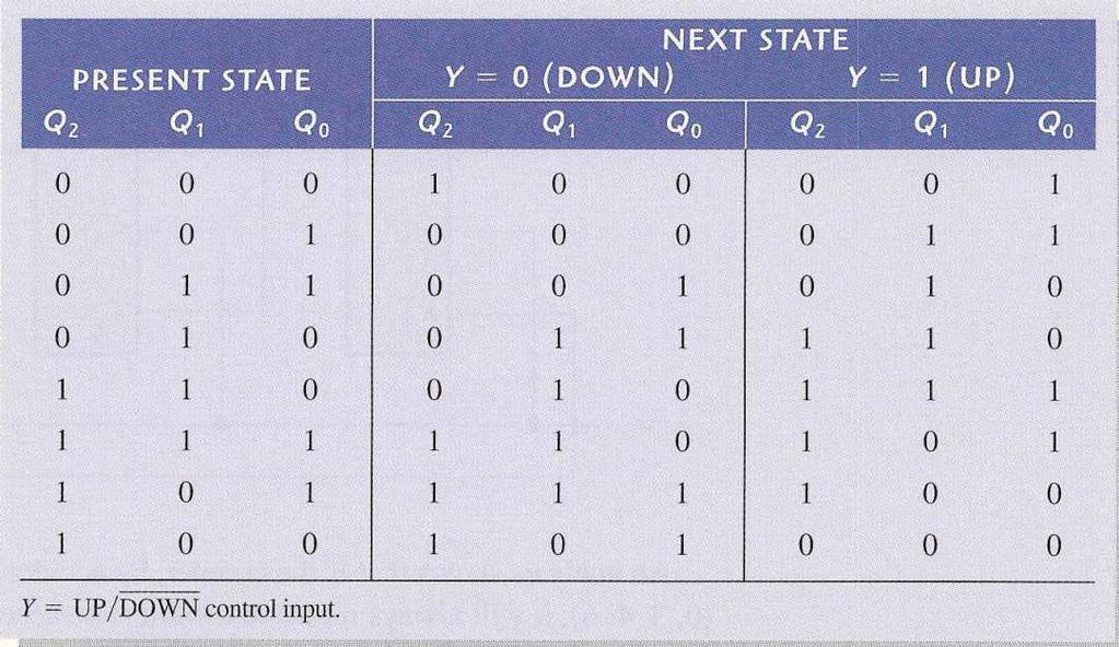
23 Up/Down Synchronous ounters Q0 toggles on every clock pulse for both UP and DOWN Q1 toggles when Q0 = 1 for UP AND when Q0 = 0 for DOWN Q2 toggles when Q0=Q1=1 for UP AND when Q0=Q1=0 for DOWN
24 Up/Down Synchronous ounters An up/down counter is capable of progressing in either direction depending on a control input. UP/DOWN HIGH J 0 UP. UP FF0 FF1 FF2 J 1 J 2 Q 1 K 0 Q 1 K 1 K 2 LK DOWN. DOWN Example waveforms from Multisim are on the next slide

25 Up/Down Synchronous ounters Q 1 UP/DOWN ount up ount down
26 Up/Down Synchronous ounters D 0 D 1 D 2 D 3 Data inputs The 74H190 is a high speed MOS synchronous up/down decade counter with parallel load capability. It also has a active LOW ripple clock output (RO) and a MAX/MIN output when the terminal count is reached. TEN D/U LOAD LK (4) (5) (11) (14) 74H190 (15) (1) (10) (9) TR DIV 10 (3) (2) (6) (7) Q 1 Q 3 D 0 D 1 D 2 D 3 (12) (13) MAX/MIN RO Data outputs Data inputs The 74H191 has the same inputs and outputs but is a synchronous up/down binary counter. TEN D/U LOAD LK (4) (5) (11) (14) 74H191 (15) (1) (10) (9) TR DIV 16 (3) (2) (6) (7) (12) (13) MAX/MIN RO Q 1 Q 3 Data outputs
27 Synchronous ounter Design
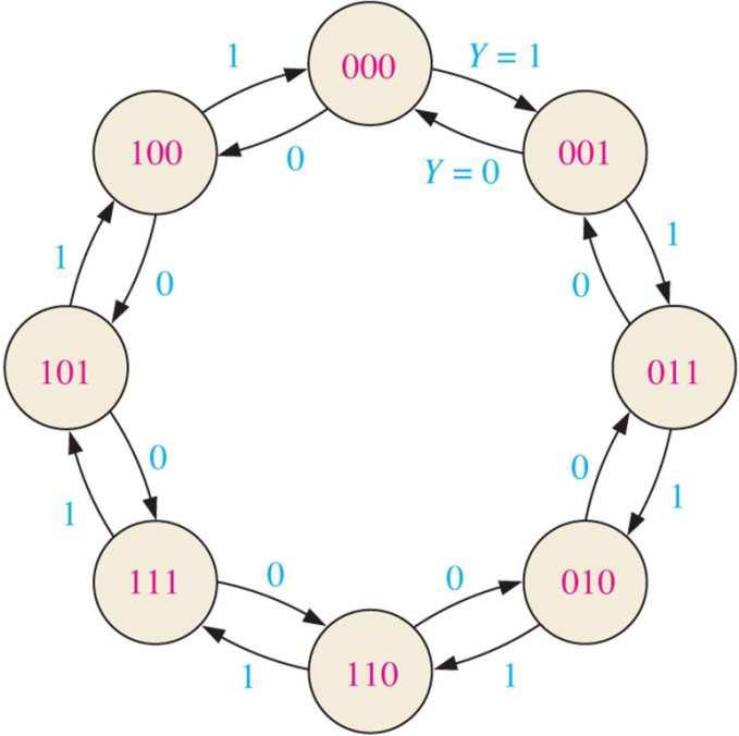
28 Synchronous ounter Design Most requirements for synchronous counters can be met with available Is. In cases where a special sequence is needed, you can apply a step-by-step design process. The steps in design are described in detail in the text and lab manual. Start with the desired sequence and draw a state diagram and nextstate table. The gray code sequence from the text is illustrated: State diagram: Next state table: Present State Q 1 Next State Q
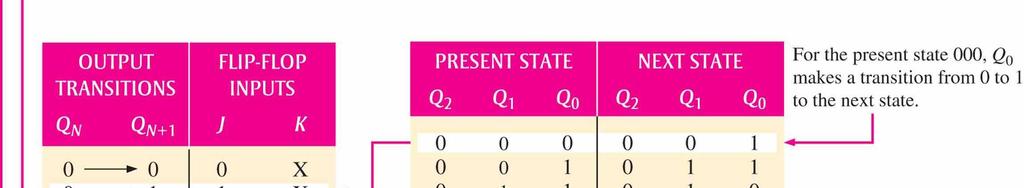
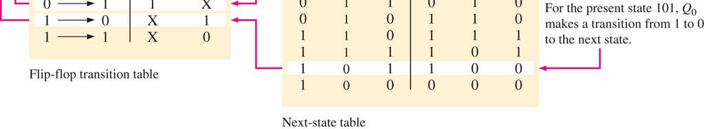
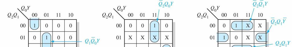
29 Summary Synchronous ounter Design The J-K transition table lists all combinations of present output (Q N ) and next output (Q N+1 ) on the left. The inputs that produce that transition are listed on the right. Each time a flip-flop is clocked, the J and K inputs required for that transition are mapped onto a K-map. An example of the J 0 map is: Q X X X X J 0 map Q 1 Q 1 Output Transitions Q N Q N Flip-Flop Inputs J K 0 X 1 X X 1 X 0 The logic for each input is read and the circuit is constructed. The next slide shows the implementation details of the circuit for the gray code counter
30 Synchronous ounter Design
31 Synchronous ounter Design
32 Synchronous ounter Design J 0 FF0 FF1 FF2 J 1 J Q 1 2 K 0 Q K 1 Q 1 K 2 2 LK The circuit can be checked with Multisim before constructing it. The next slide shows the Multisim result
33 Q 1
34 Synchronous 3-bit Up/Down Gray ode ounter
35 Synchronous 3-bit Up/Down Gray ode ounter
36 Synchronous 3-bit Up/Down Gray ode ounter
37 ascaded counters ascading is a method of achieving higher-modulus counters. For synchronous I counters, the next counter is enabled only when the terminal count of the previous stage is reached. HIGH ounter 1 ounter 2 16 TEN T TEN LK Q 1 f in TR DIV 16 TR DIV 16 ƒ in Q 3 Q 1 Q 3 T f out ƒ in 256 a) What is the modulus of the cascaded DIV 16 counters? b) If f in =100 khz, what is f out? a) Each counter divides the frequency by 16. Thus the modulus is 16 2 = 256. b) The output frequency is 100 khz/256 = 391 Hz

38 ounter Decoding Decoding is the detection of a binary number and can be done with an AND gate. HIGH Summary J 0 J 1 Q 1 J 2 Q 2 K 0 Q Q 0 1 K 1 Q 1 K 2 LK What number is decoded by this gate? LSB Decoded 4 Q Q 1 0 MSB
39 Partial Decoding Summary The decade counter shown previously incorporates partial decoding (looking at only the MSB and the LSB) to detect This was possible because this is the first occurrence of this combination in the sequence. Detects 1001 by looking only at two bits HIGH FF0 FF1 FF2 FF3 J 0 J 1 Q 1 J 2 J 3 Q 3 K 0 K 1 Q 1 K 2 K 3 Q 3 Q 3 LK
40 Resetting the ount with a Decoder The divide-by-60 counter in the text also uses partial decoding to clear the tens count when a 6 was detected. HIGH LR TR DIV 10 TEN T = 9 RO LR LR TR DIV 6 TEN LK Decode 6 To next counter Q 3 Q 1 Q 3 Q 1 Decode 59 T = 59 To ENABLE of next TR units The divide characteristic illustrated here is a good way to obtain a lower frequency using a counter. For example, the 60 Hz power line can be converted to 1 Hz. tens
41 ounter Decoding Show how to decode state 5 with an active LOW output. HIGH J 0 Q 0 J 1 Q 1 J 2 Q 2 K 0 K 1 Q 1 Q 1 K 2 LK Notice that a NAND gate was used to give the active LOW output LSB Decoded 5 Q 1 MSB


42 Decoding Glitches Glitches was produced due to the propagation delays from the decoding process Summary

43 Decoding Glitches
44 ounter Applications
Digital Fundamentals
 Digital Fundamentals Tenth Edition Floyd Chapter 9 Sections 9-1 thru 9-5 2009 Pearson Education, Upper 2008 Pearson Saddle River, Education NJ 07458. All Rights Reserved ET285 Agenda Week 2 Quiz 0: Covered
CHW 261: Logic Design
 CHW 26: Logic Design Instructors: Prof. Hala Zayed Dr. Ahmed Shalaby http://www.bu.edu.eg/staff/halazayed4 http://bu.edu.eg/staff/ahmedshalaby4# Slide Digital Fundamentals CHAPTER 8 Counters Slide 2 Counting
PGT104 Digital Electronics. PGT104 Digital Electronics
 1 Part 6 Sequential Logic ircuits Disclaimer: Most of the contents (if not all) are extracted from resources available for Digital Fundamentals 10 th Edition 2 Basic Shift Register Operations A shift register
Digital Circuits ECS 371
 Digital Circuits ECS 371 Dr. Prapun Suksompong prapun@siit.tu.ac.th Lecture 18 Office Hours: BKD 3601-7 Monday 9:00-10:30, 1:30-3:30 Tuesday 10:30-11:30 1 Announcement Reading Assignment: Chapter 7: 7-1,
COEN 312 DIGITAL SYSTEMS DESIGN - LECTURE NOTES Concordia University
 1 OEN 312 DIGIAL SYSEMS DESIGN - LEURE NOES oncordia University hapter 6: Registers and ounters NOE: For more examples and detailed description of the material in the lecture notes, please refer to the
LOGIC CIRCUITS. Basic Experiment and Design of Electronics
 Basic Experiment and Design of Electronics LOGIC CIRCUITS Ho Kyung Kim, Ph.D. hokyung@pusan.ac.kr School of Mechanical Engineering Pusan National University Outline Combinational logic circuits Output
LOGIC CIRCUITS. Basic Experiment and Design of Electronics. Ho Kyung Kim, Ph.D.
 Basic Experiment and Design of Electronics LOGIC CIRCUITS Ho Kyung Kim, Ph.D. hokyung@pusan.ac.kr School of Mechanical Engineering Pusan National University Digital IC packages TTL (transistor-transistor
Roger L. Tokheim. Chapter 8 Counters Glencoe/McGraw-Hill
 Digital Electronics Principles & Applications Sixth Edition Roger L. Tokheim Chapter 8 Counters 2003 Glencoe/McGraw-Hill INTRODUCTION Overview of Counters Characteristics of Counters Ripple Up Counter
Chapter #7: Sequential Logic Case Studies Contemporary Logic Design
 hapter #7: Sequential Logic ase Studies ontemporary Logic Design No. 7- Storage egister Group of storage elements read/written as a unit 4-bit register constructed from 4 D FFs Shared clock and clear lines
DE58/DC58 LOGIC DESIGN DEC 2014
 Q.2 a. In a base-5 number system, 3 digit representations is used. Find out (i) Number of distinct quantities that can be represented.(ii) Representation of highest decimal number in base-5. Since, r=5
EECS150 - Digital Design Lecture 18 - Counters
 EECS150 - Digital Design Lecture 18 - Counters October 24, 2002 John Wawrzynek Fall 2002 EECS150 - Lec18-counters Page 1 Counters Special sequential circuits (FSMs) that sequence though a set outputs.
EECS150 - Digital Design Lecture 18 - Counters
 EECS50 - Digital Design Lecture 8 - Counters October 24, 2002 John Wawrzynek Fall 2002 EECS50 - Lec8-counters Page Counters Special sequential circuits (FSMs) that sequence though a set outputs. Examples:
Chapter 14 Sequential logic, Latches and Flip-Flops
 Chapter 14 Sequential logic, Latches and Flip-Flops Flops Lesson 4 JK Flip Flop Ch14L4-"Digital Principles and Design", Raj Kamal, Pearson Education, 2006 2 JK Flip-Flop ve edge triggered Output Q and
NOTE: The Flatpak version has the same pinouts (Connection Diagram) as the Dual In-Line Package. *MR for LS160A and LS161A *SR for LS162A and LS163A
 as the Dual In-Line Package. *MR for LS160A and LS161A *SR for LS162A and LS163A") BCD DECADE COUNTERS/ 4-BIT BINARY COUNTERS The LS160A/ 161A/ 162A/ 163A are high-speed 4-bit synchronous counters. They are edge-triggered, synchronously presettable, and cascadable MSI building blocks
BCD DECADE COUNTERS/ 4-BIT BINARY COUNTERS The LS160A/ 161A/ 162A/ 163A are high-speed 4-bit synchronous counters. They are edge-triggered, synchronously presettable, and cascadable MSI building blocks
S.Y. Diploma : Sem. III [DE/ED/EI/EJ/EN/ET/EV/EX/IC/IE/IS/IU/MU] Principles of Digital Techniques
![S.Y. Diploma : Sem. III [DE/ED/EI/EJ/EN/ET/EV/EX/IC/IE/IS/IU/MU] Principles of Digital Techniques](/thumbs/82/86792063.jpg "S.Y. Diploma : Sem. III [DE/ED/EI/EJ/EN/ET/EV/EX/IC/IE/IS/IU/MU] Principles of Digital Techniques") S.Y. Diploma : Sem. III [DE/ED/EI/EJ/EN/ET/EV/EX/IC/IE/IS/IU/MU] Principles of Digital Techniques Time: 3 Hrs.] Prelim Question Paper Solution [Marks : 100 Q.1(a) Attempt any SIX of the following : [12]
S.Y. Diploma : Sem. III [DE/ED/EI/EJ/EN/ET/EV/EX/IC/IE/IS/IU/MU] Principles of Digital Techniques Time: 3 Hrs.] Prelim Question Paper Solution [Marks : 100 Q.1(a) Attempt any SIX of the following : [12]
ECE 341. Lecture # 3
 ECE 341 Lecture # 3 Instructor: Zeshan Chishti zeshan@ece.pdx.edu October 7, 2013 Portland State University Lecture Topics Counters Finite State Machines Decoders Multiplexers Reference: Appendix A of
Digital Electronics Final Examination. Part A
 Digital Electronics Final Examination Part A Spring 2009 Student Name: Date: Class Period: Total Points: /50 Converted Score: /40 Page 1 of 13 Directions: This is a CLOSED BOOK/CLOSED NOTES exam. Select
ECE/Comp Sci 352 Digital Systems Fundamentals. Charles R. Kime Section 2 Fall Logic and Computer Design Fundamentals
 University of Wisconsin - Madison ECE/Comp Sci 352 Digital Systems Fundamentals Charles R. Kime Section 2 Fall 2001 Lecture 5 Registers & Counters Part 2 Charles Kime Counters Counters are sequential circuits
King Fahd University of Petroleum and Minerals College of Computer Science and Engineering Computer Engineering Department
 King Fahd University of Petroleum and Minerals College of Computer Science and Engineering Computer Engineering Department Page 1 of 13 COE 202: Digital Logic Design (3-0-3) Term 112 (Spring 2012) Final
EECS150 - Digital Design Lecture 17 - Sequential Circuits 3 (Counters)
") EECS150 - Digital Design Lecture 17 - Sequential Circuits 3 (Counters) March 19&21, 2002 John Wawrzynek Spring 2002 EECS150 - Lec13-seq3 version 2 Page 1 Counters Special sequential circuits (FSMs) that
EECS150 - Digital Design Lecture 17 - Sequential Circuits 3 (Counters) March 19&21, 2002 John Wawrzynek Spring 2002 EECS150 - Lec13-seq3 version 2 Page 1 Counters Special sequential circuits (FSMs) that
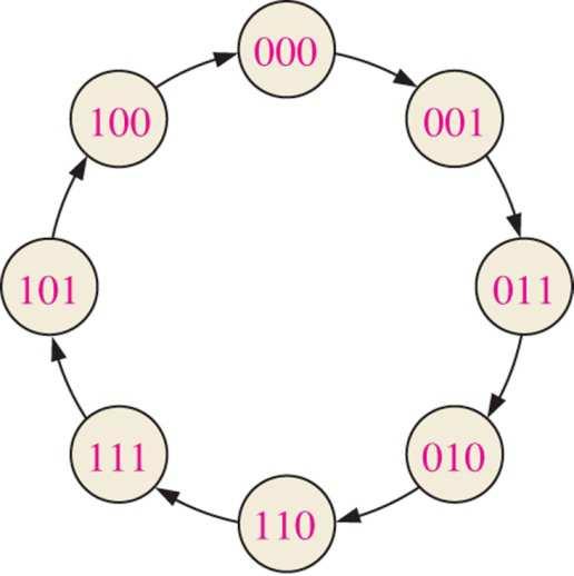
10/12/2016. An FSM with No Inputs Moves from State to State. ECE 120: Introduction to Computing. Eventually, the States Form a Loop
 University of Illinois at Urbana-Champaign Dept. of Electrical and Computer Engineering An FSM with No Inputs Moves from State to State What happens if an FSM has no inputs? ECE 120: Introduction to Computing
WORKBOOK. Try Yourself Questions. Electrical Engineering Digital Electronics. Detailed Explanations of
 27 WORKBOOK Detailed Eplanations of Try Yourself Questions Electrical Engineering Digital Electronics Number Systems and Codes T : Solution Converting into decimal number system 2 + 3 + 5 + 8 2 + 4 8 +
Synchronous 4 Bit Counters; Binary, Direct Reset
 Synchronous 4 Bit Counters; Binary, Direct Reset This synchronous, presettable counter features an internal carry look-ahead for application in high-speed counting designs. Synchronous operation is provided
S.Y. Diploma : Sem. III [CO/CM/IF/CD/CW] Digital Techniques
![S.Y. Diploma : Sem. III [CO/CM/IF/CD/CW] Digital Techniques](/thumbs/90/103932933.jpg "S.Y. Diploma : Sem. III [CO/CM/IF/CD/CW] Digital Techniques") S.Y. Diploma : Sem. III [CO/CM/IF/CD/CW] Digital Techniques Time: 3 Hrs.] Prelim Question Paper Solution [Marks : 100 Q.1(a) Attempt any SIX of the following : [12] Q.1(a) (i) Derive AND gate and OR gate
S.Y. Diploma : Sem. III [CO/CM/IF/CD/CW] Digital Techniques Time: 3 Hrs.] Prelim Question Paper Solution [Marks : 100 Q.1(a) Attempt any SIX of the following : [12] Q.1(a) (i) Derive AND gate and OR gate
MOSIS REPORT. Spring MOSIS Report 1. MOSIS Report 2. MOSIS Report 3
 MOSIS REPORT Spring 2010 MOSIS Report 1 MOSIS Report 2 MOSIS Report 3 MOSIS Report 1 Design of 4-bit counter using J-K flip flop I. Objective The purpose of this project is to design one 4-bit counter
Exam for Physics 4051, October 31, 2008
 Exam for Physics 45, October, 8 5 points - closed book - calculators allowed - show your work Problem : (6 Points) The 4 bit shift register circuit shown in Figure has been initialized to contain the following
Digital Logic Design - Chapter 4
 Digital Logic Design - Chapter 4 1. Analyze the latch circuit shown below by obtaining timing diagram for the circuit; include propagation delays. Y This circuit has two external input and one feedback
EECS150 - Digital Design Lecture 23 - FSMs & Counters
 EECS150 - Digital Design Lecture 23 - FSMs & Counters April 8, 2010 John Wawrzynek Spring 2010 EECS150 - Lec22-counters Page 1 One-hot encoding of states. One FF per state. State Encoding Why one-hot encoding?
Digital Electronics. Part A
 Digital Electronics Final Examination Part A Winter 2004-05 Student Name: Date: lass Period: Total Points: Multiple hoice Directions: Select the letter of the response which best completes the item or
INTEGRATED CIRCUITS. For a complete data sheet, please also download:
 INTEGRATED CIRCUITS DATA SEET For a complete data sheet, please also download: The IC6 74C/CT/CU/CMOS ogic Family Specifications The IC6 74C/CT/CU/CMOS ogic Package Information The IC6 74C/CT/CU/CMOS ogic
Delhi Noida Bhopal Hyderabad Jaipur Lucknow Indore Pune Bhubaneswar Kolkata Patna Web: Ph:
 Serial : S_CS_C_Digital Logic_588 Delhi Noida hopal Hyderabad Jaipur Lucknow Indore Pune hubaneswar Kolkata Patna Web: E-mail: info@madeeasy.in Ph: -56 CLASS TEST 8-9 COMPUTER SCIENCE & IT Subject : Digital
King Fahd University of Petroleum and Minerals College of Computer Science and Engineering Computer Engineering Department
 King Fahd University of Petroleum and Minerals College of Computer Science and Engineering Computer Engineering Department Page of COE 22: Digital Logic Design (3--3) Term (Fall 22) Final Exam Sunday January
EE 209 Logic Cumulative Exam Name:
 EE 209 Logic Cumulative Exam Name: 1.) Answer the following questions as True or False a.) A 4-to-1 multiplexer requires at least 4 select lines: true / false b.) An 8-to-1 mux and no other logi can be
MATC DIGITAL ELECTRONICS LAB ASYNCHRONOUS RIPPLE COUNTERS
 MT IGITL ELETONIS L SYNHONOUS IPPLE OUNTES Submitted to: Mr. Pham Submitted by: Jody ecker Submitted on: //00 Performed on: //00 Lab Group # OJETIVES Jody ecker Elctec 0-00 Lab synchronous ounters Page
EECS150 - Digital Design Lecture 11 - Shifters & Counters. Register Summary
 EECS50 - Digital Design Lecture - Shifters & Counters February 24, 2003 John Wawrzynek Spring 2005 EECS50 - Lec-counters Page Register Summary All registers (this semester) based on Flip-flops: q 3 q 2
I. Motivation & Examples
 I. Motivation & Examples Output depends on current input and past history of inputs. State embodies all the information about the past needed to predict current output based on current input. State variables,
Different encodings generate different circuits
 FSM State Encoding Different encodings generate different circuits no easy way to find best encoding with fewest logic gates or shortest propagation delay. Binary encoding: K states need log 2 K bits i.e.,
Synchronous Sequential Logic
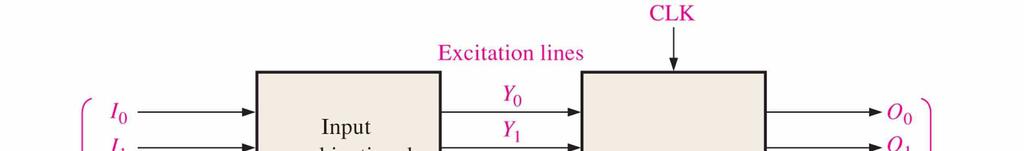
 1 IT 201 DIGITAL SYSTEMS DESIGN MODULE4 NOTES Synchronous Sequential Logic Sequential Circuits - A sequential circuit consists of a combinational circuit and a feedback through the storage elements in
Decoding A Counter. svbitec.wordpress.com 1
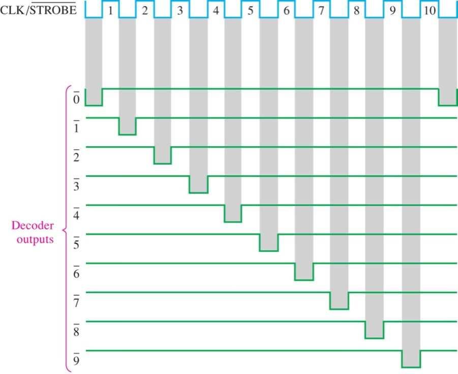
 ecoding A ounter ecoding a counter involves determining which state in the sequence the counter is in. ifferentiate between active-high and active-low decoding. Active-HIGH decoding: output HIGH if the
Digital Fundamentals
 Digital Fundamentals Tenth Edition Floyd hapter 5 Modified by Yuttapong Jiraraksopakun Floyd, Digital Fundamentals, 10 th 2008 Pearson Education ENE, KMUTT ed 2009 2009 Pearson Education, Upper Saddle
ELCT201: DIGITAL LOGIC DESIGN
 ELCT201: DIGITAL LOGIC DESIGN Dr. Eng. Haitham Omran, haitham.omran@guc.edu.eg Dr. Eng. Wassim Alexan, wassim.joseph@guc.edu.eg Following the slides of Dr. Ahmed H. Madian Lecture 10 محرم 1439 ه Winter
Counters. We ll look at different kinds of counters and discuss how to build them
 Counters We ll look at different kinds of counters and discuss how to build them These are not only examples of sequential analysis and design, but also real devices used in larger circuits 1 Introducing
Vidyalankar S.E. Sem. III [ETRX] Digital Circuits and Design Prelim Question Paper Solution
![Vidyalankar S.E. Sem. III [ETRX] Digital Circuits and Design Prelim Question Paper Solution](/thumbs/79/79145081.jpg "Vidyalankar S.E. Sem. III [ETRX] Digital Circuits and Design Prelim Question Paper Solution") S.E. Sem. III [ETRX] Digital Circuits and Design Prelim uestion Paper Solution. (a) Static Hazard Static hazards have two cases: static and static. static- hazard exists when the output variable should
S.E. Sem. III [ETRX] Digital Circuits and Design Prelim uestion Paper Solution. (a) Static Hazard Static hazards have two cases: static and static. static- hazard exists when the output variable should
Experiment 9 Sequential Circuits
 Introduction to Counters Experiment 9 Sequential Circuits The aim of this experiment is to familiarize you, frst with the basic sequential circuit device called a fip fop, and then, with the design and
Sample Test Paper - I
 Scheme G Sample Test Paper - I Course Name : Computer Engineering Group Marks : 25 Hours: 1 Hrs. Q.1) Attempt any THREE: 09 Marks a) Define i) Propagation delay ii) Fan-in iii) Fan-out b) Convert the following:
S.E. Sem. III [ETRX] Digital Circuit Design. t phl. Fig.: Input and output voltage waveforms to define propagation delay times.
![S.E. Sem. III [ETRX] Digital Circuit Design. t phl. Fig.: Input and output voltage waveforms to define propagation delay times.](/thumbs/93/111090909.jpg "S.E. Sem. III [ETRX] Digital Circuit Design. t phl. Fig.: Input and output voltage waveforms to define propagation delay times.") S.E. Sem. III [ETRX] Digital ircuit Design Time : 3 Hrs.] Prelim Paper Solution [Marks : 80. Solve following : [20].(a) Explain characteristics of logic families. [5] haracteristics of logic families are
S.E. Sem. III [ETRX] Digital ircuit Design Time : 3 Hrs.] Prelim Paper Solution [Marks : 80. Solve following : [20].(a) Explain characteristics of logic families. [5] haracteristics of logic families are
Digital Electronics Circuits 2017
 JSS SCIENCE AND TECHNOLOGY UNIVERSITY Digital Electronics Circuits (EC37L) Lab in-charge: Dr. Shankraiah Course outcomes: After the completion of laboratory the student will be able to, 1. Simplify, design
Lab 3 Revisited. Zener diodes IAP 2008 Lecture 4 1
 Lab 3 Revisited Zener diodes R C 6.091 IAP 2008 Lecture 4 1 Lab 3 Revisited +15 Voltage regulators 555 timers 270 1N758 0.1uf 5K pot V+ V- 2N2222 0.1uf V o. V CC V Vin s = 5 V Vc V c Vs 1 e t = RC Threshold
Chapter 5 Synchronous Sequential Logic
 Chapter 5 Synchronous Sequential Logic Sequential circuit: A circuit that includes memory elements. In this case the output depends not only on the current input but also on the past inputs. Memory A synchronous
COE 202: Digital Logic Design Sequential Circuits Part 4. Dr. Ahmad Almulhem ahmadsm AT kfupm Phone: Office:
 COE 202: Digital Logic Design Sequential Circuits Part 4 Dr. Ahmad Almulhem Email: ahmadsm AT kfupm Phone: 860-7554 Office: 22-324 Objectives Registers Counters Registers 0 1 n-1 A register is a group
CHW 261: Logic Design
 CHW 26: Logic Design Instructors: Prof. Hala Zayed Dr. Ahmed Shalaby http://www.bu.edu.eg/staff/halazayed4 http://bu.edu.eg/staff/ahmedshalaby4# Slide Digital Fundamentals Digital Concepts Slide 2 What?
EET 310 Flip-Flops 11/17/2011 1
 EET 310 Flip-Flops 11/17/2011 1 FF s and some Definitions Clock Input: FF s are controlled by a trigger or Clock signal. All FF s have a clock input. If a device which attempts to do a FF s task does not
Up/down binary counter with separate up/down clocks
 FEATURES Synchronous reversible 4-bit counting Asynchronous parallel load capability Asynchronous reset (clear) Cascadable without external logic DESCRIPTION The is a 4-bit synchronous up/down counter
CS221: Digital Design. Dr. A. Sahu. Indian Institute of Technology Guwahati
 CS221: Digital Design Counter&Registers Dr. A. Sahu DeptofComp.Sc.&Engg. Indian Institute of Technology Guwahati Outline Counter : Synchronous Vs Asynchronous Counter: Finite it State t Machine Mhi A register
ECEN 248: INTRODUCTION TO DIGITAL SYSTEMS DESIGN. Week 9 Dr. Srinivas Shakkottai Dept. of Electrical and Computer Engineering
 ECEN 248: INTRODUCTION TO DIGITAL SYSTEMS DESIGN Week 9 Dr. Srinivas Shakkottai Dept. of Electrical and Computer Engineering TIMING ANALYSIS Overview Circuits do not respond instantaneously to input changes
74F193 Up/Down Binary Counter with Separate Up/Down Clocks
 April 1988 Revised September 2000 Up/Down Binary Counter with Separate Up/Down Clocks General Description The is an up/down modulo-16 binary counter. Separate Count Up and Count Down Clocks are used, and
課程名稱 : 數位邏輯設計 P-1/ /6/11
 課程名稱 : 數位邏輯設計 P-1/41 2012/6/11 extbook: igital esign, 4 th. Edition M. Morris Mano and Michael. iletti Prentice-Hall, Inc. 教師 : 蘇慶龍 INSRUOR : HING-LUNG SU E-mail: kevinsu@yuntech.edu.tw hapter 6 P-2/41
Sequential vs. Combinational
 Sequential Circuits Sequential vs. Combinational Combinational Logic: Output depends only on current input TV channel selector (-9) inputs system outputs Sequential Logic: Output depends not only on current
INTEGRATED CIRCUITS. For a complete data sheet, please also download:
 INTEGRATED CIRCUITS DATA SHEET For a complete data sheet, please also download: The IC6 74HC/HCT/HCU/HCMOS ogic Family Specifications The IC6 74HC/HCT/HCU/HCMOS ogic Package Information The IC6 74HC/HCT/HCU/HCMOS
MAHALAKSHMI ENGINEERING COLLEGE TIRUCHIRAPALLI
 DEPARTMENT: ECE MAHALAKSHMI ENGINEERING COLLEGE TIRUCHIRAPALLI 6 QUESTION BANK SUBJECT NAME: DIGITAL ELECTRONICS UNIT : Design of Sequential Circuits PART A ( Marks). Draw the logic diagram 4: Multiplexer.(AUC
Chapter 7. Sequential Circuits Registers, Counters, RAM
 Chapter 7. Sequential Circuits Registers, Counters, RAM Register - a group of binary storage elements suitable for holding binary info A group of FFs constitutes a register Commonly used as temporary storage
Digital Circuits ECS 371. Dr. Prapun Suksompong Latches and Flip-Flops
 Digital Circuits ECS 371 Dr. Prapun Suksompong prapun@siit.tu.ac.th Latches and Flip-Flops 1 2 Digital Logic Circuit Types Combinational Circuit Output depends only on current inputs No feedback loops
EECS150 - Digital Design Lecture 16 Counters. Announcements
 EECS150 - Digital Design Lecture 16 Counters October 20, 2011 Elad Alon Electrical Engineering and Computer Sciences University of California, Berkeley http://www-inst.eecs.berkeley.edu/~cs150 Fall 2011
MAHARASHTRA STATE BOARD OF TECHNICAL EDUCATION (Autonomous) (ISO/IEC Certified) State any two Boolean laws. (Any 2 laws 1 mark each)
 (ISO/IEC Certified) State any two Boolean laws. (Any 2 laws 1 mark each)") Subject Code: 17333 Model Answer Page 1/ 27 Important Instructions to examiners: 1) The answers should be examined by key words and not as word-to-word as given in the model answer scheme. 2) The model
Subject Code: 17333 Model Answer Page 1/ 27 Important Instructions to examiners: 1) The answers should be examined by key words and not as word-to-word as given in the model answer scheme. 2) The model
Introduction EE 224: INTRODUCTION TO DIGITAL CIRCUITS & COMPUTER DESIGN. Lecture 6: Sequential Logic 3 Registers & Counters 5/9/2010
 EE 224: INTROUCTION TO IGITAL CIRCUITS & COMPUTER ESIGN Lecture 6: Sequential Logic 3 Registers & Counters 05/10/2010 Avinash Kodi, kodi@ohio.edu Introduction 2 A Flip-Flop stores one bit of information
Fundamentals of Computer Systems
 Fundamentals of Computer Systems Sequential Logic Stephen A. Edwards Columbia University Summer 2017 State-Holding Elements Bistable Elements S Latch Latch Positive-Edge-Triggered Flip-Flop Flip-Flop with
Computers also need devices capable of Storing data and information Performing mathematical operations on such data
 Sequential Machines Introduction Logic devices examined so far Combinational Output function of input only Output valid as long as input true Change input change output Computers also need devices capable
SIR C.R.REDDY COLLEGE OF ENGINEERING ELURU DIGITAL INTEGRATED CIRCUITS (DIC) LABORATORY MANUAL III / IV B.E. (ECE) : I - SEMESTER
 LABORATORY MANUAL III / IV B.E. (ECE) : I - SEMESTER") SIR C.R.REDDY COLLEGE OF ENGINEERING ELURU 534 007 DIGITAL INTEGRATED CIRCUITS (DIC) LABORATORY MANUAL III / IV B.E. (ECE) : I - SEMESTER DEPARTMENT OF ELECTRONICS AND COMMUNICATION ENGINEERING DIGITAL
SIR C.R.REDDY COLLEGE OF ENGINEERING ELURU 534 007 DIGITAL INTEGRATED CIRCUITS (DIC) LABORATORY MANUAL III / IV B.E. (ECE) : I - SEMESTER DEPARTMENT OF ELECTRONICS AND COMMUNICATION ENGINEERING DIGITAL
INTEGRATED CIRCUITS. For a complete data sheet, please also download:
 INTEGRATED CIRCUITS DATA SHEET For a complete data sheet, please also download: The IC06 74HC/HCT/HCU/HCMOS Logic Family Specifications The IC06 74HC/HCT/HCU/HCMOS Logic Package Information The IC06 74HC/HCT/HCU/HCMOS
INTEGRATED CIRCUITS. For a complete data sheet, please also download:
 INTEGRATED CIRCUITS DATA SEET For a complete data sheet, please also download: The IC0 74C/CT/CU/CMOS ogic Family Specifications The IC0 74C/CT/CU/CMOS ogic Package Information The IC0 74C/CT/CU/CMOS ogic
The Design Procedure. Output Equation Determination - Derive output equations from the state table
 The Design Procedure Specification Formulation - Obtain a state diagram or state table State Assignment - Assign binary codes to the states Flip-Flop Input Equation Determination - Select flipflop types
EECS150 - Digital Design Lecture 25 Shifters and Counters. Recap
 EECS150 - Digital Design Lecture 25 Shifters and Counters Nov. 21, 2013 Prof. Ronald Fearing Electrical Engineering and Computer Sciences University of California, Berkeley (slides courtesy of Prof. John
Dr. Nicola Nicolici COE/EE2DI4 Midterm Test #2 Nov 22, 2006
 COE/EE2DI4 Midterm Test #2 Fall 2006 Page 1 Dr. Nicola Nicolici COE/EE2DI4 Midterm Test #2 Nov 22, 2006 Instructions: This examination paper includes 12 pages and 20 multiple-choice questions starting
CSE370 HW6 Solutions (Winter 2010)
") SE370 HW6 Solutions (Winter 2010) 1. L2e, 6.10 For this problem we are given a blank waveform with clock and input and asked to draw out the how different flip-flops and latches would behave. LK a) b)
SE370 HW6 Solutions (Winter 2010) 1. L2e, 6.10 For this problem we are given a blank waveform with clock and input and asked to draw out the how different flip-flops and latches would behave. LK a) b)
Preparation of Examination Questions and Exercises: Solutions
 Questions Preparation of Examination Questions and Exercises: Solutions. -bit Subtraction: DIF = B - BI B BI BO DIF 2 DIF: B BI 4 6 BI 5 BO: BI BI 4 5 7 3 2 6 7 3 B B B B B DIF = B BI ; B = ( B) BI ( B),
Digital Electronics. Delay Max. FF Rate Power/Gate High Low (ns) (MHz) (mw) (V) (V) Standard TTL (7400)
 (MHz) (mw) (V) (V) Standard TTL (7400)") P57/67 Lec9, P Digital Electronics Introduction: In electronics we can classify the building blocks of a circuit or system as being either analog or digital in nature. If we focus on voltage as the circuit
P57/67 Lec9, P Digital Electronics Introduction: In electronics we can classify the building blocks of a circuit or system as being either analog or digital in nature. If we focus on voltage as the circuit
Show that the dual of the exclusive-or is equal to its compliment. 7
 Darshan Institute of ngineering and Technology, Rajkot, Subject: Digital lectronics (2300) GTU Question ank Unit Group Questions Do as directed : I. Given that (6)0 = (00)x, find the value of x. II. dd
Layout of 7400-series Chips Commonly Used in. CDA 3101: Introduction to Computer Hardware and Organization
 Layout of 400-series Chips Commonly Used in CDA 30: Introduction to Computer Hardware and Organization Charles N. Winton Department of Computer and Information Sciences University of North Florida 999
Gates and Flip-Flops
 Gates and Flip-Flops Chris Kervick (11355511) With Evan Sheridan and Tom Power December 2012 On a scale of 1 to 10, how likely is it that this question is using binary?...4? What s a 4? Abstract The operation
6 Synchronous State Machine Design
 Design of synchronous counters. Based on the description of the problem, determine the required number n of the FFs - the smallest value of n is such that the number of states N 2 n and the desired counting
74LS195 SN74LS195AD LOW POWER SCHOTTKY
 The SN74LS95A is a high speed 4-Bit Shift Register offering typical shift frequencies of 39 MHz. It is useful for a wide variety of register and counting applications. It utilizes the Schottky diode clamped
ELCT201: DIGITAL LOGIC DESIGN
 ELCT201: DIGITAL LOGIC DESIGN Dr. Eng. Haitham Omran, haitham.omran@guc.edu.eg Dr. Eng. Wassim Alexan, wassim.joseph@guc.edu.eg Lecture 6 Following the slides of Dr. Ahmed H. Madian محرم 1439 ه Winter
Unit 7 Sequential Circuits (Flip Flop, Registers)
") College of Computer and Information Sciences Department of Computer Science CSC 220: Computer Organization Unit 7 Sequential Circuits (Flip Flop, Registers) 2 SR Flip-Flop The SR flip-flop, also known
College of Computer and Information Sciences Department of Computer Science CSC 220: Computer Organization Unit 7 Sequential Circuits (Flip Flop, Registers) 2 SR Flip-Flop The SR flip-flop, also known
Overview of Chapter 4
 Overview of hapter 4 Types of Sequential ircuits Storage Elements Latches Flip-Flops Sequential ircuit Analysis State Tables State Diagrams Sequential ircuit Design Specification Assignment of State odes
Sequential Logic Circuits
 Chapter 4 Sequential Logic Circuits 4 1 The defining characteristic of a combinational circuit is that its output depends only on the current inputs applied to the circuit. The output of a sequential circuit,
Introduction to Digital Logic
 Introduction to Digital Logic Lecture 17: Latches Flip-Flops Problem w/ Bistables Output should have been at end of sequence Problem: Glitch was remembered Need some way to ignore inputs until they are
Unit II Chapter 4:- Digital Logic Contents 4.1 Introduction... 4
 Unit II Chapter 4:- Digital Logic Contents 4.1 Introduction... 4 4.1.1 Signal... 4 4.1.2 Comparison of Analog and Digital Signal... 7 4.2 Number Systems... 7 4.2.1 Decimal Number System... 7 4.2.2 Binary
Synchronous Sequential Circuit Design. Digital Computer Design
 Synchronous Sequential Circuit Design Digital Computer Design Races and Instability Combinational logic has no cyclic paths and no races If inputs are applied to combinational logic, the outputs will always
Review: Designing with FSM. EECS Components and Design Techniques for Digital Systems. Lec 09 Counters Outline.
 Review: esigning with FSM EECS 150 - Components and esign Techniques for igital Systems Lec 09 Counters 9-28-0 avid Culler Electrical Engineering and Computer Sciences University of California, Berkeley
Philadelphia University Student Name: Student Number:
 Philadelphia University Student Name: Student Number: Faculty of Engineering Serial Number: Final Exam, First Semester: 2017/2018 Dept. of Computer Engineering Course Title: Logic Circuits Date: 29/01/2018
Lecture 3 Review on Digital Logic (Part 2)
") Lecture 3 Review on Digital Logic (Part 2) Xuan Silvia Zhang Washington University in St. Louis http://classes.engineering.wustl.edu/ese461/ ircuit Optimization Simplest implementation ost criterion literal
Lecture 3 Review on Digital Logic (Part 2) Xuan Silvia Zhang Washington University in St. Louis http://classes.engineering.wustl.edu/ese461/ ircuit Optimization Simplest implementation ost criterion literal
DATA SHEET. HEF40163B MSI 4-bit synchronous binary counter with synchronous reset. For a complete data sheet, please also download:
 INTEGRATED CIRCUITS DATA SHEET For a complete data sheet, please also download: The IC04 LOCMOS HE4000B Logic Family Specifications HEF, HEC The IC04 LOCMOS HE4000B Logic Package Outlines/Information HEF,
MICROCIRCUITS, DIGITAL, LOW-POWER SCHOTTKY TTL, COUNTERS, MONOLITHIC SILICON. Inactive for new design after 18 April 1997.
 INCH-POUND MIL-M-38510/315D 27 October 2003 SUPERSEDING MIL-M-38510/315C 17 JANUARY 1984 MILITARY SPECIFICATION MICROCIRCUITS, DIGITAL, LOW-POWER SCHOTTKY TTL, COUNTERS, MONOLITHIC SILICON This specification
Design of Sequential Circuits
 Design of Sequential Circuits Seven Steps: Construct a state diagram (showing contents of flip flop and inputs with next state) Assign letter variables to each flip flop and each input and output variable
Standard Products UT54ACS190/UT54ACTS190 Synchronous 4-Bit Up-Down BCD Counters. Datasheet November
 Standard Products UT54AS190/UT54ATS190 Synchronous 4-Bit Up-Down BD ounters Datasheet November 2010 www.aeroflex.com/logic FEATURES Single down/up count control line Look-ahead circuitry enhances speed
Review: Designing with FSM. EECS Components and Design Techniques for Digital Systems. Lec09 Counters Outline.
 Review: Designing with FSM EECS 150 - Components and Design Techniques for Digital Systems Lec09 Counters 9-28-04 David Culler Electrical Engineering and Computer Sciences University of California, Berkeley
Chapter 7 Sequential Logic
 Chapter 7 Sequential Logic SKEE2263 Digital Systems Mun im/ismahani/izam {munim@utm.my,e-izam@utm.my,ismahani@fke.utm.my} March 28, 2016 Table of Contents 1 Intro 2 Bistable Circuits 3 FF Characteristics
Time Allowed 3:00 hrs. April, pages
 IGITAL ESIGN COEN 32 Prof. r. A. J. Al-Khalili Time Allowed 3: hrs. April, 998 2 pages Answer All uestions No materials are allowed uestion a) esign a half subtractor b) esign a full subtractor c) Using
Sequential Logic. Rab Nawaz Khan Jadoon DCS. Lecturer COMSATS Lahore Pakistan. Department of Computer Science
 Sequential Logic Rab Nawaz Khan Jadoon DCS COMSATS Institute of Information Technology Lecturer COMSATS Lahore Pakistan Digital Logic and Computer Design Sequential Logic Combinational circuits with memory
Stop Watch (System Controller Approach)
") Stop Watch (System Controller Approach) Problem Design a stop watch that can measure times taken for two events Inputs CLK = 6 Hz RESET: Asynchronously reset everything X: comes from push button First
Stop Watch (System Controller Approach) Problem Design a stop watch that can measure times taken for two events Inputs CLK = 6 Hz RESET: Asynchronously reset everything X: comes from push button First