Lab 3 Revisited. Zener diodes IAP 2008 Lecture 4 1
|
|
|
- Leslie Woods
- 5 years ago
- Views:
Transcription
1 Lab 3 Revisited Zener diodes R C IAP 2008 Lecture 4 1
2 Lab 3 Revisited +15 Voltage regulators 555 timers 270 1N uf 5K pot V+ V- 2N uf V o. V CC V Vin s = 5 V Vc V c Vs 1 e t = RC Threshold Control Voltage Trigger k 5k 5k 1 Gnd + Comp _ A + Comp _ B R S Flip Flop Inhibit/ Reset 4 Reset 7 3 Discharge Output IAP 2008 Lecture 4 Figure by MIT OpenCourseWare. 2
3 Closet Light Timer k reset 10k 555 output R threshold 1N914 trigger discharge 1k 0.1uf control C uf IAP 2008 Lecture 4 3
4 Digital Circuits Real world analog signals have noise unavoidable. Digital circuits offers better noise immunity. Use voltage to represent 0 and 1 Avoid forbidden voltage zone. Make standards tighter for output than for inputs. Data (HCMOS family): 0 (low), 1 (high) Input voltage low: v Input voltage high: >2.0V Output low: <0.4v Output high: >3.98v IAP 2008 Lecture 4 4
5 Digital Circuits +5V HCMOS 1 (high) Output high: >3.98v output high range +3.98V Input voltage high: >2.0V input high range noise margin +2.0V Forbidden Zone HCMOS 0 (low) 0.7V Output low: <0.4v Input voltage low: v noise margin output low range 0.4V input low rage IAP 2008 Lecture 4 5
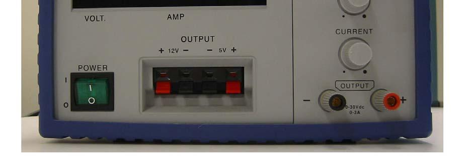
6 Power Requirements The following power supplies are common for analog and digital circuits: +5v for digital circuits, +15v, -15v for analog, -5v, +12v, -12v also used +3.3 Other voltages generally derived IAP 2008 Lecture 4 6


7 6.091 IAP 2008 Lecture 4 7
8 Boolean Algebra A B = A & B A = Inverse of A A B = Inverse of [A&B] DeMorgan's Law A B = A + B A + B = A & B IAP 2008 Lecture 4 8
9 Digital System Implementation Start with AND, OR, NOR, NAND gates and add more complex building blocks: registers, counters, shift registers, multiplexers. Wire up design. High manufacturing cost, low fix costs. Examples 74LS, 74HC series IC For volume production, move to PALs, FPGAs, ASICs. Low manufacturing cost, high fix costs IAP 2008 Lecture 4 9
10 Basic Gates Circle indicates inversion IAP 2008 Lecture 4 10
11 74LS00 NAND Gate Dual-In-Line Package V CC B4 A4 Y4 B3 A3 Y A1 B1 Y1 A2 B2 Y2 GND This device contains four independent gates each of which performs the logic NAND function. Figure by MIT OpenCourseWare, adapted from the National Semiconductor 54LS00 datasheet IAP 2008 Lecture 4 11
12 74LS02 NOR Gate Dual-In-Line Package V CC Y4 B4 A4 Y3 B3 A Y1 A1 B1 Y2 A2 B2 GND This device contains four independent gates each of which performs the logic NOR function. Figure by MIT OpenCourseWare, adapted from the National Semiconductor 54LS02 datasheet IAP 2008 Lecture 4 12
13 74LS08 AND Gate Dual-In-Line Package VCC B4 A4 Y4 B3 A3 Y A1 B1 Y1 A2 B2 Y2 GND This device contains four independent gates each of which performs the logic AND function. Figure by MIT OpenCourseWare, adapted from the National Semiconductor 54LS08 datasheet IAP 2008 Lecture 4 13
14 74LS Multiplexer Dual-in-line Package Data Inputs Data Select VCC D4 D5 D6 D7 A B C Inputs Select C B A X X X L L L L L H L H L L H H H L L H L H H H L H H H Strobe S H L L L L L L L L Outputs Y L D0 D1 D2 D3 D4 D5 D6 D7 W H D0 D1 D2 D3 D4 D5 D6 D7 D3 D2 D1 D0 Y W Strobe GND H = High Level, L = Low Level, X = Don t Care D0, D1_D7 = Level of the Respective D Input Data Inputs Outputs Figures by MIT OpenCourseWare IAP 2008 Lecture 4 14
15 Building Logic From basic gates, we can build other functions: Exclusive OR Gate X Y Z X Y Z X Y Z IAP 2008 Lecture 4 15
16 74LS86 Exclusive OR V CC Truth Table GND In Out A L L H H B L H L H Z L H H L Figure by MIT OpenCourseWare, based on Motorola datasheet IAP 2008 Lecture 4 16
17 74LS74 D Flip Flop SET-PRESET Note both and bar CLK D SET CLR CLR circle indicates inversion (active low) Reprinted with permission of National Semiconductor Corporation. CLK D IAP 2008 Lecture 4 17
18 Counters Ripple carry Previous stage used to clock next bit; B 1 B CLK D B 0 SET CLR D B 1 SET CLR Synchronous B 0 B 1 Same clock used for each bit D SET D SET CLR CLR Power connections not shown CLK IAP 2008 Lecture 4 18
19 Building a Synchronous Counter All bits clock on the same clock signal. Next count based on current count. B 1 B 0 B 1 Next B 0 B 1 D SET D SET CLK CLR CLR Power connections not shown B 1 Next IAP 2008 Lecture 4 19
20 Shift Register DATA D SET D D SET C D SET B D SET CLR CLR CLR CLR CLK DATA D C B Converts serial data to parallel data or parallel data to serial data. A IAP 2008 Lecture 4 20
21 74LS175 4 Bit Shift Register D SET D SET 74LS D SET Clock and Clear are common for all FF. The D FF will store the state of 7 their individual D inputs on D SET the LOW to HIGH Clock transition, causing the individual and to follow. CLR CLR clock clear CLR CLR A LOW input on the Clear will force all outputs LOW and outputs HIGH independent of Clock or Data inputs IAP 2008 Lecture 4 21
22 Binary Numbers MSB Most Significant Bit LSB Least Significant Bit Let s build an adder: A+B=S where A,B,S are m bits wide: A: A m A m-1 A 1 A 0 Dec Binary Hex Dec Binary Hex A B C D E F IAP 2008 Lecture 4 22
23 Binary Adder m th bit C in A B Sum C out A B C in ADDER C out Sum Sum = C out = IAP 2008 Lecture 4 23
24 Signed Numbers Twos Complement Positive Number: MSB=0 Negative Number: MSB=1 4 Bit example Simple addition & subtraction Most common notation MSB LSB Decimal IAP 2008 Lecture 4 24

25 Propagation Delays All digital logic have propagation delay Typical discrete logic gate propagation delay ~10ns X Z X Z IAP 2008 Lecture 4 25
26 Lab Exercise Ring Oscillator IAP 2008 Lecture 4 26
27 Lab Exercise 4 Bit Counter Logic Analyzer +5 Power connections not shown for 74LS Mhz crystal osc P T LD CLR 74LS163 counter A B C D Attach LA probe A2 to A-D triangle is symbol for clock input IAP 2008 Lecture 4 27
28 Lab Exercise Ramp Generator R R R R V o R 2R 2R 2R 2R +5 B Mhz crystal osc P T LD A B C CLR D 74LS163 counter A B C D B 1 74HC08 B 2 B 3 triangle is symbol for clock input IAP 2008 Lecture 4 28
29 RAMP Generator Output IAP 2008 Lecture 4 29
30 R-2R Theory For linear circuits, superposition applies. Calculate contribute of bit n by setting all other inputs to zero. Equivalent resistance looking left or right is R ohms! Use Thevenin equivalent to show division by 2 n R same as R ohms same as R ohms same as R ohms R R R R 2R 2R 2R 2R +5V V o IAP 2008 Lecture 4 30
31 DA Summary Output from digital to analog conversion are discrete levels. More bits means better resolution. An example of DA conversion Current audio CD s have 16 bit resolution or 65,536 possible output levels New DVD audio samples at 192 khz with 24 bit resolution or 2 24 = 16,777, IAP 2008 Lecture 4 31
32 Analog to Digital Conversion (ADC) Successive approximate conversion steps Scale the input to 0-3 volts (example) Sample and hold the input Internally generate and star case ramp and compare Flash Compare Compare voltage to one of 2 n possible voltage levels. 8 bit ADC would have 255 comparators. Note that by definition, ADC have quantizing errors (number of bits resolution) IAP 2008 Lecture 4 32

33 Successive Approximation AD L14, Fall IAP 2008 Lecture 4 33
34 AD7871 Courtesy of Analog Devices. Used with permission IAP 2008 Lecture 4 34
35 Switch Bounce All mechanical switches have switch bounce +5V Vout IAP 2008 Lecture 4 35
36 Debounce Circuit +5v 1K T 1K +5v bar T B bar SPDT switch B Requires SPDT switch IAP 2008 Lecture 4 36
37 Lab 4 Use last three aisles on the left at the end of the lab Pick up IC s and tools from LA s. Return IC s and tools to LA s at the end of the lab IAP 2008 Lecture 4 37


38 Design, build and keep the electronics for a digital lock. Unlock key based on sequence of 0, 1. Lab IAP 2008 Lecture 4 38
LOGIC CIRCUITS. Basic Experiment and Design of Electronics. Ho Kyung Kim, Ph.D.
 Basic Experiment and Design of Electronics LOGIC CIRCUITS Ho Kyung Kim, Ph.D. hokyung@pusan.ac.kr School of Mechanical Engineering Pusan National University Digital IC packages TTL (transistor-transistor
Sample Test Paper - I
 Scheme G Sample Test Paper - I Course Name : Computer Engineering Group Marks : 25 Hours: 1 Hrs. Q.1) Attempt any THREE: 09 Marks a) Define i) Propagation delay ii) Fan-in iii) Fan-out b) Convert the following:
MAHARASHTRA STATE BOARD OF TECHNICAL EDUCATION (Autonomous) (ISO/IEC Certified) State any two Boolean laws. (Any 2 laws 1 mark each)
 (ISO/IEC Certified) State any two Boolean laws. (Any 2 laws 1 mark each)") Subject Code: 17333 Model Answer Page 1/ 27 Important Instructions to examiners: 1) The answers should be examined by key words and not as word-to-word as given in the model answer scheme. 2) The model
Subject Code: 17333 Model Answer Page 1/ 27 Important Instructions to examiners: 1) The answers should be examined by key words and not as word-to-word as given in the model answer scheme. 2) The model
S.Y. Diploma : Sem. III [CO/CM/IF/CD/CW] Digital Techniques
![S.Y. Diploma : Sem. III [CO/CM/IF/CD/CW] Digital Techniques](/thumbs/90/103932933.jpg "S.Y. Diploma : Sem. III [CO/CM/IF/CD/CW] Digital Techniques") S.Y. Diploma : Sem. III [CO/CM/IF/CD/CW] Digital Techniques Time: 3 Hrs.] Prelim Question Paper Solution [Marks : 100 Q.1(a) Attempt any SIX of the following : [12] Q.1(a) (i) Derive AND gate and OR gate
S.Y. Diploma : Sem. III [CO/CM/IF/CD/CW] Digital Techniques Time: 3 Hrs.] Prelim Question Paper Solution [Marks : 100 Q.1(a) Attempt any SIX of the following : [12] Q.1(a) (i) Derive AND gate and OR gate
Lecture 9: Digital Electronics
 Introduction: We can classify the building blocks of a circuit or system as being either analog or digital in nature. If we focus on voltage as the circuit parameter of interest: nalog: The voltage can
LOGIC CIRCUITS. Basic Experiment and Design of Electronics
 Basic Experiment and Design of Electronics LOGIC CIRCUITS Ho Kyung Kim, Ph.D. hokyung@pusan.ac.kr School of Mechanical Engineering Pusan National University Outline Combinational logic circuits Output
Digital Circuits. 1. Inputs & Outputs are quantized at two levels. 2. Binary arithmetic, only digits are 0 & 1. Position indicates power of 2.
 Digital Circuits 1. Inputs & Outputs are quantized at two levels. 2. inary arithmetic, only digits are 0 & 1. Position indicates power of 2. 11001 = 2 4 + 2 3 + 0 + 0 +2 0 16 + 8 + 0 + 0 + 1 = 25 Digital
Exam for Physics 4051, October 31, 2008
 Exam for Physics 45, October, 8 5 points - closed book - calculators allowed - show your work Problem : (6 Points) The 4 bit shift register circuit shown in Figure has been initialized to contain the following
Experiment 9 Sequential Circuits
 Introduction to Counters Experiment 9 Sequential Circuits The aim of this experiment is to familiarize you, frst with the basic sequential circuit device called a fip fop, and then, with the design and
Fundamentals of Digital Design
 Fundamentals of Digital Design Digital Radiation Measurement and Spectroscopy NE/RHP 537 1 Binary Number System The binary numeral system, or base-2 number system, is a numeral system that represents numeric
CHW 261: Logic Design
 CHW 26: Logic Design Instructors: Prof. Hala Zayed Dr. Ahmed Shalaby http://www.bu.edu.eg/staff/halazayed4 http://bu.edu.eg/staff/ahmedshalaby4# Slide Digital Fundamentals CHAPTER 8 Counters Slide 2 Counting
S.Y. Diploma : Sem. III [DE/ED/EI/EJ/EN/ET/EV/EX/IC/IE/IS/IU/MU] Principles of Digital Techniques
![S.Y. Diploma : Sem. III [DE/ED/EI/EJ/EN/ET/EV/EX/IC/IE/IS/IU/MU] Principles of Digital Techniques](/thumbs/82/86792063.jpg "S.Y. Diploma : Sem. III [DE/ED/EI/EJ/EN/ET/EV/EX/IC/IE/IS/IU/MU] Principles of Digital Techniques") S.Y. Diploma : Sem. III [DE/ED/EI/EJ/EN/ET/EV/EX/IC/IE/IS/IU/MU] Principles of Digital Techniques Time: 3 Hrs.] Prelim Question Paper Solution [Marks : 100 Q.1(a) Attempt any SIX of the following : [12]
S.Y. Diploma : Sem. III [DE/ED/EI/EJ/EN/ET/EV/EX/IC/IE/IS/IU/MU] Principles of Digital Techniques Time: 3 Hrs.] Prelim Question Paper Solution [Marks : 100 Q.1(a) Attempt any SIX of the following : [12]
Reg. No. Question Paper Code : B.E./B.Tech. DEGREE EXAMINATION, NOVEMBER/DECEMBER Second Semester. Computer Science and Engineering
 Sp 6 Reg. No. Question Paper Code : 27156 B.E./B.Tech. DEGREE EXAMINATION, NOVEMBER/DECEMBER 2015. Second Semester Computer Science and Engineering CS 6201 DIGITAL PRINCIPLES AND SYSTEM DESIGN (Common
ENGG 1203 Tutorial _03 Laboratory 3 Build a ball counter. Lab 3. Lab 3 Gate Timing. Lab 3 Steps in designing a State Machine. Timing diagram of a DFF
 ENGG 1203 Tutorial _03 Laboratory 3 Build a ball counter Timing diagram of a DFF Lab 3 Gate Timing difference timing for difference kind of gate, cost dependence (1) Setup Time = t2-t1 (2) Propagation
EE40 Lec 15. Logic Synthesis and Sequential Logic Circuits
 EE40 Lec 15 Logic Synthesis and Sequential Logic Circuits Prof. Nathan Cheung 10/20/2009 Reading: Hambley Chapters 7.4-7.6 Karnaugh Maps: Read following before reading textbook http://www.facstaff.bucknell.edu/mastascu/elessonshtml/logic/logic3.html
Digital Electronic Meters
 Digital Electronic Meters EIE 240 Electrical and Electronic Measurement May 1, 2015 1 Digital Signal Binary or two stages: 0 (Low voltage 0-3 V) 1 (High voltage 4-5 V) Binary digit is called bit. Group
Roger L. Tokheim. Chapter 8 Counters Glencoe/McGraw-Hill
 Digital Electronics Principles & Applications Sixth Edition Roger L. Tokheim Chapter 8 Counters 2003 Glencoe/McGraw-Hill INTRODUCTION Overview of Counters Characteristics of Counters Ripple Up Counter
Digital Electronics. Delay Max. FF Rate Power/Gate High Low (ns) (MHz) (mw) (V) (V) Standard TTL (7400)
 (MHz) (mw) (V) (V) Standard TTL (7400)") P57/67 Lec9, P Digital Electronics Introduction: In electronics we can classify the building blocks of a circuit or system as being either analog or digital in nature. If we focus on voltage as the circuit
P57/67 Lec9, P Digital Electronics Introduction: In electronics we can classify the building blocks of a circuit or system as being either analog or digital in nature. If we focus on voltage as the circuit
Schedule. ECEN 301 Discussion #25 Final Review 1. Date Day Class No. 1 Dec Mon 25 Final Review. Title Chapters HW Due date. Lab Due date.
 Schedule Date Day Class No. Dec Mon 25 Final Review 2 Dec Tue 3 Dec Wed 26 Final Review Title Chapters HW Due date Lab Due date LAB 8 Exam 4 Dec Thu 5 Dec Fri Recitation HW 6 Dec Sat 7 Dec Sun 8 Dec Mon
MAHARASHTRA STATE BOARD OF TECHNICAL EDUCATION (Autonomous) (ISO/IEC Certified)
 (ISO/IEC Certified)") WINTER 17 EXAMINATION Subject Name: Digital Techniques Model Answer Subject Code: 17333 Important Instructions to examiners: 1) The answers should be examined by key words and not as word-to-word as given
WINTER 17 EXAMINATION Subject Name: Digital Techniques Model Answer Subject Code: 17333 Important Instructions to examiners: 1) The answers should be examined by key words and not as word-to-word as given
on candidate s understanding. 7) For programming language papers, credit may be given to any other program based on equivalent concept.
 For programming language papers, credit may be given to any other program based on equivalent concept.") WINTER 17 EXAMINATION Subject Name: Digital Techniques Model Answer Subject Code: 17333 Important Instructions to examiners: 1) The answers should be examined by key words and not as word-to-word as given
WINTER 17 EXAMINATION Subject Name: Digital Techniques Model Answer Subject Code: 17333 Important Instructions to examiners: 1) The answers should be examined by key words and not as word-to-word as given
Vidyalankar S.E. Sem. III [CMPN] Digital Logic Design and Analysis Prelim Question Paper Solution
![Vidyalankar S.E. Sem. III [CMPN] Digital Logic Design and Analysis Prelim Question Paper Solution](/thumbs/90/103673562.jpg "Vidyalankar S.E. Sem. III [CMPN] Digital Logic Design and Analysis Prelim Question Paper Solution") . (a) (i) ( B C 5) H (A 2 B D) H S.E. Sem. III [CMPN] Digital Logic Design and Analysis Prelim Question Paper Solution ( B C 5) H (A 2 B D) H = (FFFF 698) H (ii) (2.3) 4 + (22.3) 4 2 2. 3 2. 3 2 3. 2 (2.3)
. (a) (i) ( B C 5) H (A 2 B D) H S.E. Sem. III [CMPN] Digital Logic Design and Analysis Prelim Question Paper Solution ( B C 5) H (A 2 B D) H = (FFFF 698) H (ii) (2.3) 4 + (22.3) 4 2 2. 3 2. 3 2 3. 2 (2.3)
Digital Fundamentals
 Digital Fundamentals Tenth Edition Floyd Chapter 9 Sections 9-1 thru 9-5 2009 Pearson Education, Upper 2008 Pearson Saddle River, Education NJ 07458. All Rights Reserved ET285 Agenda Week 2 Quiz 0: Covered
WORKBOOK. Try Yourself Questions. Electrical Engineering Digital Electronics. Detailed Explanations of
 27 WORKBOOK Detailed Eplanations of Try Yourself Questions Electrical Engineering Digital Electronics Number Systems and Codes T : Solution Converting into decimal number system 2 + 3 + 5 + 8 2 + 4 8 +
Digital Electronics Final Examination. Part A
 Digital Electronics Final Examination Part A Spring 2009 Student Name: Date: Class Period: Total Points: /50 Converted Score: /40 Page 1 of 13 Directions: This is a CLOSED BOOK/CLOSED NOTES exam. Select
University of Florida EEL 3701 Fall 2014 Dr. Eric. M. Schwartz Department of Electrical & Computer Engineering Wednesday, 15 October 2014
 Page 1/12 Exam 1 May the Schwartz Instructions: be with you! Turn off all cell phones and other noise making devices and put away all electronics Show all work on the front of the test papers Box each
CHW 261: Logic Design
 CHW 26: Logic Design Instructors: Prof. Hala Zayed Dr. Ahmed Shalaby http://www.bu.edu.eg/staff/halazayed4 http://bu.edu.eg/staff/ahmedshalaby4# Slide Digital Fundamentals Digital Concepts Slide 2 What?
Digital Circuits ECS 371
 Digital Circuits ECS 371 Dr. Prapun Suksompong prapun@siit.tu.ac.th Lecture 18 Office Hours: BKD 3601-7 Monday 9:00-10:30, 1:30-3:30 Tuesday 10:30-11:30 1 Announcement Reading Assignment: Chapter 7: 7-1,
Delhi Noida Bhopal Hyderabad Jaipur Lucknow Indore Pune Bhubaneswar Kolkata Patna Web: Ph:
 Serial : S_CS_C_Digital Logic_588 Delhi Noida hopal Hyderabad Jaipur Lucknow Indore Pune hubaneswar Kolkata Patna Web: E-mail: info@madeeasy.in Ph: -56 CLASS TEST 8-9 COMPUTER SCIENCE & IT Subject : Digital
 vidyarthiplus.com vidyarthiplus.com vidyarthiplus.com ANNA UNIVERSITY- COMBATORE B.E./ B.TECH. DEGREE EXAMINATION - JUNE 2009. ELECTRICAL & ELECTONICS ENGG. - FOURTH SEMESTER DIGITAL LOGIC CIRCUITS PART-A
DIGITAL LOGIC CIRCUITS
 DIGITAL LOGIC CIRCUITS Digital logic circuits BINARY NUMBER SYSTEM electronic circuits that handle information encoded in binary form (deal with signals that have only two values, and ) Digital. computers,
Digital Electronics. Part A
 Digital Electronics Final Examination Part A Winter 2004-05 Student Name: Date: lass Period: Total Points: Multiple hoice Directions: Select the letter of the response which best completes the item or
Gates and Flip-Flops
 Gates and Flip-Flops Chris Kervick (11355511) With Evan Sheridan and Tom Power December 2012 On a scale of 1 to 10, how likely is it that this question is using binary?...4? What s a 4? Abstract The operation
Digital Signal 2 N Most Significant Bit (MSB) Least. Bit (LSB)
 Least. Bit (LSB)") 1 Digital Signal Binary or two stages: 0 (Low voltage 0-3 V) 1 (High voltage 4-5 V) Binary digit is called bit. Group of bits is called word. 8-bit group is called byte. For N-bit base-2 number = 2 N levels
1 Digital Signal Binary or two stages: 0 (Low voltage 0-3 V) 1 (High voltage 4-5 V) Binary digit is called bit. Group of bits is called word. 8-bit group is called byte. For N-bit base-2 number = 2 N levels
Boole Algebra and Logic Series
 S1 Teknik Telekomunikasi Fakultas Teknik Elektro oole lgebra and Logic Series 2016/2017 CLO1-Week2-asic Logic Operation and Logic Gate Outline Understand the basic theory of oolean Understand the basic
NOTE: The Flatpak version has the same pinouts (Connection Diagram) as the Dual In-Line Package. *MR for LS160A and LS161A *SR for LS162A and LS163A
 as the Dual In-Line Package. *MR for LS160A and LS161A *SR for LS162A and LS163A") BCD DECADE COUNTERS/ 4-BIT BINARY COUNTERS The LS160A/ 161A/ 162A/ 163A are high-speed 4-bit synchronous counters. They are edge-triggered, synchronously presettable, and cascadable MSI building blocks
BCD DECADE COUNTERS/ 4-BIT BINARY COUNTERS The LS160A/ 161A/ 162A/ 163A are high-speed 4-bit synchronous counters. They are edge-triggered, synchronously presettable, and cascadable MSI building blocks
Digital Electronics Circuits 2017
 JSS SCIENCE AND TECHNOLOGY UNIVERSITY Digital Electronics Circuits (EC37L) Lab in-charge: Dr. Shankraiah Course outcomes: After the completion of laboratory the student will be able to, 1. Simplify, design
University of Florida EEL 3701 Summer 2015 Dr. Eric. M. Schwartz Department of Electrical & Computer Engineering Tuesday, 30 June 2015
 University of Florida EEL 3701 Summer 2015 Dr Eric M Schwartz Page 1/13 Exam 1 May the Schwartz be with you! Instructions: Turn off all cell phones and other noise making devices Show all work on the front
MAHARASHTRA STATE BOARD OF TECHNICAL EDUCATION (Autonomous) (ISO/IEC Certified) SUMMER 14 EXAMINATION Model Answer
 (ISO/IEC Certified) SUMMER 14 EXAMINATION Model Answer") MAHARASHTRA STATE BOARD OF TECHNICAL EDUCATION (Autonomous) (ISO/IEC 27001 2005 Certified) SUMMER 14 EXAMINATION Model Answer Subject Code : 17320 Page No: 1/34 Important Instructions to examiners: 1)
MAHARASHTRA STATE BOARD OF TECHNICAL EDUCATION (Autonomous) (ISO/IEC 27001 2005 Certified) SUMMER 14 EXAMINATION Model Answer Subject Code : 17320 Page No: 1/34 Important Instructions to examiners: 1)
Preparation of Examination Questions and Exercises: Solutions
 Questions Preparation of Examination Questions and Exercises: Solutions. -bit Subtraction: DIF = B - BI B BI BO DIF 2 DIF: B BI 4 6 BI 5 BO: BI BI 4 5 7 3 2 6 7 3 B B B B B DIF = B BI ; B = ( B) BI ( B),
74LS195 SN74LS195AD LOW POWER SCHOTTKY
 The SN74LS95A is a high speed 4-Bit Shift Register offering typical shift frequencies of 39 MHz. It is useful for a wide variety of register and counting applications. It utilizes the Schottky diode clamped
DE58/DC58 LOGIC DESIGN DEC 2014
 Q.2 a. In a base-5 number system, 3 digit representations is used. Find out (i) Number of distinct quantities that can be represented.(ii) Representation of highest decimal number in base-5. Since, r=5
Synchronous 4 Bit Counters; Binary, Direct Reset
 Synchronous 4 Bit Counters; Binary, Direct Reset This synchronous, presettable counter features an internal carry look-ahead for application in high-speed counting designs. Synchronous operation is provided
Unit II Chapter 4:- Digital Logic Contents 4.1 Introduction... 4
 Unit II Chapter 4:- Digital Logic Contents 4.1 Introduction... 4 4.1.1 Signal... 4 4.1.2 Comparison of Analog and Digital Signal... 7 4.2 Number Systems... 7 4.2.1 Decimal Number System... 7 4.2.2 Binary
SUMMER 18 EXAMINATION Subject Name: Principles of Digital Techniques Model Answer Subject Code:
 Important Instructions to examiners: 1) The answers should be examined by key words and not as word-to-word as given in the model answer scheme. 2) The model answer and the answer written by candidate
04. What is the Mod number of the counter circuit shown below? Assume initially reset.
 . Which of the following is the state diagram for the Meale machine shown below. 4. What is the Mod number of the counter circuit shown below? Assume initiall reset. input CLK D output D D a. b. / / /
Vidyalankar S.E. Sem. III [EXTC] Digital Electronics Prelim Question Paper Solution ABCD ABCD ABCD ABCD ABCD ABCD ABCD ABCD = B
![Vidyalankar S.E. Sem. III [EXTC] Digital Electronics Prelim Question Paper Solution ABCD ABCD ABCD ABCD ABCD ABCD ABCD ABCD = B](/thumbs/84/91058397.jpg "Vidyalankar S.E. Sem. III [EXTC] Digital Electronics Prelim Question Paper Solution ABCD ABCD ABCD ABCD ABCD ABCD ABCD ABCD = B") . (a). (b). (c) S.E. Sem. III [EXTC] igital Electronics Prelim Question Paper Solution ABC ABC ABC ABC ABC ABC ABC ABC = B LHS = ABC ABC ABC ABC ABC ABC ABC ABC But ( ) = = ABC( ) ABC( ) ABC( ) ABC( )
. (a). (b). (c) S.E. Sem. III [EXTC] igital Electronics Prelim Question Paper Solution ABC ABC ABC ABC ABC ABC ABC ABC = B LHS = ABC ABC ABC ABC ABC ABC ABC ABC But ( ) = = ABC( ) ABC( ) ABC( ) ABC( )
King Fahd University of Petroleum and Minerals College of Computer Science and Engineering Computer Engineering Department
 King Fahd University of Petroleum and Minerals College of Computer Science and Engineering Computer Engineering Department Page 1 of 13 COE 202: Digital Logic Design (3-0-3) Term 112 (Spring 2012) Final
ENGR4300 Fall 2005 Test 3S. Name solution. Section. Question 1 (25 points) Question 2 (25 points) Question 3 (25 points) Question 4 (25 points)
 Question 2 (25 points) Question 3 (25 points) Question 4 (25 points)") ENGR400 Test S Fall 005 ENGR400 Fall 005 Test S Name solution Section uestion (5 points) uestion (5 points) uestion (5 points) uestion 4 (5 points) Total (00 points): Please do not write on the crib sheets.
ENGR400 Test S Fall 005 ENGR400 Fall 005 Test S Name solution Section uestion (5 points) uestion (5 points) uestion (5 points) uestion 4 (5 points) Total (00 points): Please do not write on the crib sheets.
Sequential Logic Worksheet
 Sequential Logic Worksheet Concept Inventory: Notes: D-latch & the Dynamic Discipline D-register Timing constraints for sequential circuits Set-up and hold times for sequential circuits 6.004 Worksheet
CHAPTER 7. Exercises 17/ / /2 2 0
 CHAPTER 7 Exercises E7. (a) For the whole part, we have: Quotient Remainders 23/2 /2 5 5/2 2 2/2 0 /2 0 Reading the remainders in reverse order, we obtain: 23 0 = 0 2 For the fractional part we have 2
MM74HC161 MM74HC163 Synchronous Binary Counter with Asynchronous Clear Synchronous Binary Counter with Synchronous Clear
 September 1983 Revised February 1999 MM74HC161 MM74HC163 Synchronous Binary Counter with Asynchronous Clear Synchronous Binary Counter with Synchronous Clear General Description The MM74HC161 and MM74HC163
MM54HCT193 MM74HCT193 Synchronous Binary Up Down Counters
 MM54HCT193 MM74HCT193 Synchronous Binary Up Down Counters General Description These high speed synchronous counters utilize advanced silicon-gate CMOS technology to achieve the high noise immunity and
Lecture 7: Logic design. Combinational logic circuits
 /24/28 Lecture 7: Logic design Binary digital circuits: Two voltage levels: and (ground and supply voltage) Built from transistors used as on/off switches Analog circuits not very suitable for generic
EE 209 Logic Cumulative Exam Name:
 EE 209 Logic Cumulative Exam Name: 1.) Answer the following questions as True or False a.) A 4-to-1 multiplexer requires at least 4 select lines: true / false b.) An 8-to-1 mux and no other logi can be
INTEGRATED CIRCUITS. For a complete data sheet, please also download:
 INTEGRATED CIRCUITS DATA SHEET For a complete data sheet, please also download: The IC06 74HC/HCT/HCU/HCMOS Logic Family Specifications The IC06 74HC/HCT/HCU/HCMOS Logic Package Information The IC06 74HC/HCT/HCU/HCMOS
COEN 312 DIGITAL SYSTEMS DESIGN - LECTURE NOTES Concordia University
 1 OEN 312 DIGIAL SYSEMS DESIGN - LEURE NOES oncordia University hapter 6: Registers and ounters NOE: For more examples and detailed description of the material in the lecture notes, please refer to the
Exercise booklet - Logic
 Name: Class: Date:......... Exercise booklet Logic BCD Counter Worksheet with excercises and repetitive tasks for students and learners Find the seven logic gates in the puzzle. The words can be hidden
Dept. of ECE, CIT, Gubbi Page 1
 Verification: 1) A.B = A + B 7404 7404 7404 A B A.B A.B 0 0 0 1 0 1 0 1 1 0 0 1 1 1 1 0 A B A B A + B 0 0 1 1 1 0 1 1 0 1 1 0 0 1 1 1 1 0 0 0 2) A+B = A. B 7404 7404 7404 A B A+B A+B 0 0 0 1 0 1 1 0 1
Chapter 2 Boolean Algebra and Logic Gates
 Chapter 2 Boolean Algebra and Logic Gates The most common postulates used to formulate various algebraic structures are: 1. Closure. N={1,2,3,4 }, for any a,b N we obtain a unique c N by the operation
A Guide. Logic Library
 Logic A Guide To The Logic Library SystemView by ELANIX Copyright 1994-2005, Eagleware Corporation All rights reserved. Eagleware-Elanix Corporation 3585 Engineering Drive, Suite 150 Norcross, GA 30092
Counters. We ll look at different kinds of counters and discuss how to build them
 Counters We ll look at different kinds of counters and discuss how to build them These are not only examples of sequential analysis and design, but also real devices used in larger circuits 1 Introducing
Combinational Logic. By : Ali Mustafa
 Combinational Logic By : Ali Mustafa Contents Adder Subtractor Multiplier Comparator Decoder Encoder Multiplexer How to Analyze any combinational circuit like this? Analysis Procedure To obtain the output
Boolean Algebra and Digital Logic 2009, University of Colombo School of Computing
 IT 204 Section 3.0 Boolean Algebra and Digital Logic Boolean Algebra 2 Logic Equations to Truth Tables X = A. B + A. B + AB A B X 0 0 0 0 3 Sum of Products The OR operation performed on the products of
SAU1A FUNDAMENTALS OF DIGITAL COMPUTERS
 SAU1A FUNDAMENTALS OF DIGITAL COMPUTERS Unit : I - V Unit : I Overview Fundamentals of Computers Characteristics of Computers Computer Language Operating Systems Generation of Computers 2 Definition of
SIR C.R.REDDY COLLEGE OF ENGINEERING ELURU DIGITAL INTEGRATED CIRCUITS (DIC) LABORATORY MANUAL III / IV B.E. (ECE) : I - SEMESTER
 LABORATORY MANUAL III / IV B.E. (ECE) : I - SEMESTER") SIR C.R.REDDY COLLEGE OF ENGINEERING ELURU 534 007 DIGITAL INTEGRATED CIRCUITS (DIC) LABORATORY MANUAL III / IV B.E. (ECE) : I - SEMESTER DEPARTMENT OF ELECTRONICS AND COMMUNICATION ENGINEERING DIGITAL
SIR C.R.REDDY COLLEGE OF ENGINEERING ELURU 534 007 DIGITAL INTEGRATED CIRCUITS (DIC) LABORATORY MANUAL III / IV B.E. (ECE) : I - SEMESTER DEPARTMENT OF ELECTRONICS AND COMMUNICATION ENGINEERING DIGITAL
MOSIS REPORT. Spring MOSIS Report 1. MOSIS Report 2. MOSIS Report 3
 MOSIS REPORT Spring 2010 MOSIS Report 1 MOSIS Report 2 MOSIS Report 3 MOSIS Report 1 Design of 4-bit counter using J-K flip flop I. Objective The purpose of this project is to design one 4-bit counter
Computers also need devices capable of Storing data and information Performing mathematical operations on such data
 Sequential Machines Introduction Logic devices examined so far Combinational Output function of input only Output valid as long as input true Change input change output Computers also need devices capable
( c) Give logic symbol, Truth table and circuit diagram for a clocked SR flip-flop. A combinational circuit is defined by the function
 Give logic symbol, Truth table and circuit diagram for a clocked SR flip-flop. A combinational circuit is defined by the function") Question Paper Digital Electronics (EE-204-F) MDU Examination May 2015 1. (a) represent (32)10 in (i) BCD 8421 code (ii) Excess-3 code (iii) ASCII code (b) Design half adder using only NAND gates. ( c)
Question Paper Digital Electronics (EE-204-F) MDU Examination May 2015 1. (a) represent (32)10 in (i) BCD 8421 code (ii) Excess-3 code (iii) ASCII code (b) Design half adder using only NAND gates. ( c)
Digital Fundamentals
 Digital Fundamentals Tenth Edition Floyd hapter 8 Modified by Yuttapong Jiraraksopakun Floyd, Digital Fundamentals, 10 th 2008 Pearson Education ENE, KMUTT ed 2009 ounting in Binary As you know, the binary
INTEGRATED CIRCUITS. For a complete data sheet, please also download:
 INTEGRATED CIRCUITS DATA SHEET For a complete data sheet, please also download: The IC6 74HC/HCT/HCU/HCMOS Logic Family Specifications The IC6 74HC/HCT/HCU/HCMOS Logic Package Information The IC6 74HC/HCT/HCU/HCMOS
MAHARASHTRA STATE BOARD OF TECHNICAL EDUCATION
 MAHARASHTRA STATE BOARD OF TECHNICAL EDUCATION (Autonomous) (ISO/IEC - 27001-2005 Certified) Subject Code: 12069 SUMMER 13 EXAMINATION Model Answer Important Instructions to examiners: 1) The answers should
3. Complete the following table of equivalent values. Use binary numbers with a sign bit and 7 bits for the value
 EGC22 Digital Logic Fundamental Additional Practice Problems. Complete the following table of equivalent values. Binary. Octal 35.77 33.23.875 29.99 27 9 64 Hexadecimal B.3 D.FD B.4C 2. Calculate the following
 Distributed by: www.jameco.com 1-800-831-4242 The content and copyrights of the attached material are the property of its owner. INTEGRATED CIRCUITS DATA SHEET For a complete data sheet, please also download:
Fundamentals of Boolean Algebra
 UNIT-II 1 Fundamentals of Boolean Algebra Basic Postulates Postulate 1 (Definition): A Boolean algebra is a closed algebraic system containing a set K of two or more elements and the two operators and
Appendix B. Review of Digital Logic. Baback Izadi Division of Engineering Programs
 Appendix B Review of Digital Logic Baback Izadi Division of Engineering Programs bai@engr.newpaltz.edu Elect. & Comp. Eng. 2 DeMorgan Symbols NAND (A.B) = A +B NOR (A+B) = A.B AND A.B = A.B = (A +B ) OR
CIRCUITS AND ELECTRONICS. The Digital Abstraction
 6.002 CIRCUITS AND ELECTRONICS The Digital Abstraction Review Discretize matter by agreeing to observe the lumped matter discipline Lumped Circuit Abstraction Analysis tool kit: KVL/KCL, node method, superposition,
DIGITAL LOGIC CIRCUITS
 DIGITAL LOGIC CIRCUITS Introduction Logic Gates Boolean Algebra Map Specification Combinational Circuits Flip-Flops Sequential Circuits Memory Components Integrated Circuits Digital Computers 2 LOGIC GATES
ELCT201: DIGITAL LOGIC DESIGN
 ELCT201: DIGITAL LOGIC DESIGN Dr. Eng. Haitham Omran, haitham.omran@guc.edu.eg Dr. Eng. Wassim Alexan, wassim.joseph@guc.edu.eg Lecture 6 Following the slides of Dr. Ahmed H. Madian محرم 1439 ه Winter
Department of Electrical & Electronics EE-333 DIGITAL SYSTEMS
 Department of Electrical & Electronics EE-333 DIGITAL SYSTEMS 1) Given the two binary numbers X = 1010100 and Y = 1000011, perform the subtraction (a) X -Y and (b) Y - X using 2's complements. a) X = 1010100
EE141Microelettronica. CMOS Logic
 Microelettronica CMOS Logic CMOS logic Power consumption in CMOS logic gates Where Does Power Go in CMOS? Dynamic Power Consumption Charging and Discharging Capacitors Short Circuit Currents Short Circuit
NTE74177 Integrated Circuit TTL 35Mhz Presettable Binary Counter/Latch
 NTE74177 Integrated Circuit TTL 35Mhz Presettable Binary Counter/Latch Description: The NTE74177 is a high speed monolithic counter in a 14 Lead plastic DIP type package consisting of four DC coupled master
CPE100: Digital Logic Design I
 Professor Brendan Morris, SEB 3216, brendan.morris@unlv.edu CPE100: Digital Logic Design I Final Review http://www.ee.unlv.edu/~b1morris/cpe100/ 2 Logistics Tuesday Dec 12 th 13:00-15:00 (1-3pm) 2 hour
S.E. Sem. III [ETRX] Digital Circuit Design. t phl. Fig.: Input and output voltage waveforms to define propagation delay times.
![S.E. Sem. III [ETRX] Digital Circuit Design. t phl. Fig.: Input and output voltage waveforms to define propagation delay times.](/thumbs/93/111090909.jpg "S.E. Sem. III [ETRX] Digital Circuit Design. t phl. Fig.: Input and output voltage waveforms to define propagation delay times.") S.E. Sem. III [ETRX] Digital ircuit Design Time : 3 Hrs.] Prelim Paper Solution [Marks : 80. Solve following : [20].(a) Explain characteristics of logic families. [5] haracteristics of logic families are
S.E. Sem. III [ETRX] Digital ircuit Design Time : 3 Hrs.] Prelim Paper Solution [Marks : 80. Solve following : [20].(a) Explain characteristics of logic families. [5] haracteristics of logic families are
UNIVERSITY OF BOLTON SCHOOL OF ENGINEERING BENG (HONS) ELECTRICAL & ELECTRONICS ENGINEERING EXAMINATION SEMESTER /2017
 ELECTRICAL & ELECTRONICS ENGINEERING EXAMINATION SEMESTER /2017") UNIVERSITY OF BOLTON TW35 SCHOOL OF ENGINEERING BENG (HONS) ELECTRICAL & ELECTRONICS ENGINEERING EXAMINATION SEMESTER 2-2016/2017 INTERMEDIATE DIGITAL ELECTRONICS AND COMMUNICATIONS MODULE NO: EEE5002
UNIVERSITY OF BOLTON TW35 SCHOOL OF ENGINEERING BENG (HONS) ELECTRICAL & ELECTRONICS ENGINEERING EXAMINATION SEMESTER 2-2016/2017 INTERMEDIATE DIGITAL ELECTRONICS AND COMMUNICATIONS MODULE NO: EEE5002
Philadelphia University Student Name: Student Number:
 Philadelphia University Student Name: Student Number: Faculty of Engineering Serial Number: Final Exam, Second Semester: 2015/2016 Dept. of Computer Engineering Course Title: Logic Circuits Date: 08/06/2016
MM54HC73 MM74HC73 Dual J-K Flip-Flops with Clear
 MM54HC73 MM74HC73 Dual J-K Flip-Flops with Clear General Description These J-K Flip-Flops utilize advanced silicon-gate CMOS technology They possess the high noise immunity and low power dissipation of
PGT104 Digital Electronics. PGT104 Digital Electronics
 1 Part 6 Sequential Logic ircuits Disclaimer: Most of the contents (if not all) are extracted from resources available for Digital Fundamentals 10 th Edition 2 Basic Shift Register Operations A shift register
ECE/Comp Sci 352 Digital Systems Fundamentals. Charles R. Kime Section 2 Fall Logic and Computer Design Fundamentals
 University of Wisconsin - Madison ECE/Comp Sci 352 Digital Systems Fundamentals Charles R. Kime Section 2 Fall 2001 Lecture 5 Registers & Counters Part 2 Charles Kime Counters Counters are sequential circuits
Digital Logic. CS211 Computer Architecture. l Topics. l Transistors (Design & Types) l Logic Gates. l Combinational Circuits.
 l Logic Gates. l Combinational Circuits.") CS211 Computer Architecture Digital Logic l Topics l Transistors (Design & Types) l Logic Gates l Combinational Circuits l K-Maps Figures & Tables borrowed from:! http://www.allaboutcircuits.com/vol_4/index.html!
CS211 Computer Architecture Digital Logic l Topics l Transistors (Design & Types) l Logic Gates l Combinational Circuits l K-Maps Figures & Tables borrowed from:! http://www.allaboutcircuits.com/vol_4/index.html!
per chip (approx) 1 SSI (Small Scale Integration) Up to 99
 1 SSI (Small Scale Integration) Up to 99") Q.2 a. Classify the integration technology as per the scale of integration. Explain in brief the various steps involved in fabrication of monolithic IC. Scales of Integration (Basic) Various steps involved
Q.2 a. Classify the integration technology as per the scale of integration. Explain in brief the various steps involved in fabrication of monolithic IC. Scales of Integration (Basic) Various steps involved
Cs302 Quiz for MID TERM Exam Solved
 Question # 1 of 10 ( Start time: 01:30:33 PM ) Total Marks: 1 Caveman used a number system that has distinct shapes: 4 5 6 7 Question # 2 of 10 ( Start time: 01:31:25 PM ) Total Marks: 1 TTL based devices
ELCT201: DIGITAL LOGIC DESIGN
 ELCT201: DIGITAL LOGIC DESIGN Dr. Eng. Haitham Omran, haitham.omran@guc.edu.eg Dr. Eng. Wassim Alexan, wassim.joseph@guc.edu.eg Following the slides of Dr. Ahmed H. Madian Lecture 10 محرم 1439 ه Winter
Appendix A: Digital Logic. Principles of Computer Architecture. Principles of Computer Architecture by M. Murdocca and V. Heuring
 - Principles of Computer rchitecture Miles Murdocca and Vincent Heuring 999 M. Murdocca and V. Heuring -2 Chapter Contents. Introduction.2 Combinational Logic.3 Truth Tables.4 Logic Gates.5 Properties
Sequential Logic Circuits
 Chapter 4 Sequential Logic Circuits 4 1 The defining characteristic of a combinational circuit is that its output depends only on the current inputs applied to the circuit. The output of a sequential circuit,
Introduction EE 224: INTRODUCTION TO DIGITAL CIRCUITS & COMPUTER DESIGN. Lecture 6: Sequential Logic 3 Registers & Counters 5/9/2010
 EE 224: INTROUCTION TO IGITAL CIRCUITS & COMPUTER ESIGN Lecture 6: Sequential Logic 3 Registers & Counters 05/10/2010 Avinash Kodi, kodi@ohio.edu Introduction 2 A Flip-Flop stores one bit of information
Chapter 2. Review of Digital Systems Design
 x 2-4 = 42.625. Chapter 2 Review of Digital Systems Design Numbering Systems Decimal number may be expressed as powers of 10. For example, consider a six digit decimal number 987654, which can be represented
S.Y. Diploma : Sem. III [CO/CM/IF/CD/CW] Digital Techniques s complement 2 s complement 1 s complement
![S.Y. Diploma : Sem. III [CO/CM/IF/CD/CW] Digital Techniques s complement 2 s complement 1 s complement](/thumbs/80/82077570.jpg "S.Y. Diploma : Sem. III [CO/CM/IF/CD/CW] Digital Techniques s complement 2 s complement 1 s complement") S.Y. Diploma : Sem. III [CO/CM/IF/CD/CW] Digital Techniques Time: 3 Hrs.] Prelim Question Paper Solution [Marks : Q.(a) (i) () (2) s COMPLEMENT s COMPLEMENT 2s COMPLEMENT 2s COMPLEMENT + Q.(a) (ii) ()
S.Y. Diploma : Sem. III [CO/CM/IF/CD/CW] Digital Techniques Time: 3 Hrs.] Prelim Question Paper Solution [Marks : Q.(a) (i) () (2) s COMPLEMENT s COMPLEMENT 2s COMPLEMENT 2s COMPLEMENT + Q.(a) (ii) ()
Digital Logic Appendix A
 Digital Logic Appendix A Boolean Algebra Gates Combinatorial Circuits Sequential Circuits 1 Boolean Algebra George Boole ideas 1854 Claude Shannon, apply to circuit design, 1938 Describe digital circuitry
INTEGRATED CIRCUITS. For a complete data sheet, please also download:
 INTEGRATED CIRCUITS DATA SEET For a complete data sheet, please also download: The IC0 74C/CT/CU/CMOS Logic Family Specifications The IC0 74C/CT/CU/CMOS Logic Package Information The IC0 74C/CT/CU/CMOS