Digital EE141 Integrated Circuits 2nd Combinational Circuits
|
|
|
- Curtis Daniels
- 5 years ago
- Views:
Transcription
1 Digital Integrated Circuits Designing i Combinational Logic Circuits 1
2 Combinational vs. Sequential Logic 2
3 Static CMOS Circuit t every point in time (except during the switching transients) each gate output is connected to either V DD or V ss via a low-resistive path. The outputs of the gates assume at all times the value of the oolean function, implemented by the circuit (ignoring, once again, the transient effects during switching periods). This is in contrast to the dynamic circuit class, which relies on temporary storage of signal values on the capacitance of high impedance circuit nodes. 3
4 Static Complementary CMOS V DD In1 In2 InN In1 In2 InN PUN PDN PMOS only F(In1,In2, InN), NMOS only PUN (pull-up network) and PDN (pull-down network) are dual logic networks 4
5 NMOS Transistors in Series/Parallel l Connection Transistors can be thought as a switch controlled by its gate signal NMOS switch closes when switch control input is high X Y Y = X if and X Y Y = X if OR NMOS Transistors pass a strong 0buta weak 1 5
6 PMOS Transistors in Series/Parallel l Connection PMOS switch closes when switch control input is low X Y Y = X if ND = + X Y Y = X if OR = PMOS Transistors pass a strong 1 but a weak 0 6
7 Threshold Drops PUN V DD S V DD D V DD D 0 V S DD 0 V DD -V Tn V GS C L C L PDN V DD 0 V DD V Tp VDD D C L V GS S C L S D 7
8 Complementary CMOS Logic Style 8
9 Example Gate: NND 9
10 Example Gate: NOR 10
11 Complex CMOS Gate C D D C OUT = D + ( + C) 11
12 Constructing a Complex Gate 12
13 Cell Design Standard Cells General purpose logic Can be synthesized Same height, varying width Datapath Cells For regular, structured designs (arithmetic) Includes some wiring in the cell Fixed height and width 13
14 Standard Cell Layout Methodology 1980s Routing channel V DD signals GND 14
15 Standard Cell Layout Methodology 1990s Mirrored Cell No Routing channels V DD V DD M2 M3 GND Mirrored Cell GND 15
16 Standard Cells N Well V DD Cell height ht 12 metal tracks Metal track is approx. 3λ + 3λ Pitch = repetitive distance between objects Cell height is 12 pitch 2λ In Out Cell boundary GND Rails ~10λ 16
17 Standard Cells With minimal diffusion routing V DD With silicided diffusion V DD V DD In M 2 Out In Out In Out M 1 GND GND 17
18 Standard Cells V DD 2-input NND gate V DD Out GND 18
19 Stick Diagrams Contains no dimensions Represents relative positions of transistors Inverter V DD NND2 V DD Out Out GND In GND 19
20 Stick Diagrams j C Logic Graph X C PUN X = C (+ ) X i V DD C i j C GND PDN 20
21 Two Versions of C ( + ) C C V DD V DD X X GND GND 21
22 Consistent Euler Path X C X i V DD j GND C 22
23 OI22 Logic Graph C X PUN D D C X = (+) (C+D) X V DD C D C D GND PDN 23
24 Example: x = ab+cd x x b c b c x V DD x V DD a d a d GND GND (a) Logic graphs for (ab+cd) (b) Euler Paths {a b c d} V DD x GND a b c d (c) stick diagram for ordering {a b c d} 24
25 Multi-Fingered Transistors One finger Two fingers (folded) Less diffusion capacitance 25
26 Properties of Complementary CMOS Gates Snapshot High noise margins: V OH and V OL are at V DD and GND, respectively. No static power consumption: There never exists a direct path between V DD and V SS (GND)insteady-state state mode. Comparable rise and fall times: (under appropriate sizing conditions) 26
27 CMOS Properties Full rail-to-rail swing; high noise margins Logic levels not dependent upon the relative device sizes; ratioless lways a path to Vdd or Gnd in steady state; low output impedance Extremely high input resistance; nearly zero steady-state state input current No direct path steady state between power and ground; no static power dissipation Propagation delay function of load capacitance and resistance of transistors 27
28 Switch Delay Model R eq R p R n R p R p C L R n C L R p R p C int R R n R n C n L C NND2 R n Cint INV NOR2 28
29 Input Pattern Effects on Delay Delay is dependent on R R the pattern of inputs p p Low to high transition R n R n C L C int both inputs go low delay is 0.69 R p /2 C L one input goes low delay is 0.69 R p C L High to low transition both inputs go high h delay is R n C L 29
30 Delay Dependence on Input Patterns Vo oltage [V V] ==1 0 =1, =1 0 =1 0, = time [ps] Input Data Pattern Delay (psec) == =1 1, = = 0 1, =1 61 == =1, = = 1 0, =1 81 NMOS = 0.5μm/0.25 μm PMOS = 0.75μm/0.25 μm C L = 100 ff 30
31 Transistor Sizing R p R p R p R n C L 4 R p C int 2 R n Cint 1 R n R n 1 C L 31
32 Transistor Sizing a Complex CMOS Gate C 8 6 D 4 6 OUT = D + ( + C) 2 D 1 2 C 2 32
33 Fan-In Considerations C D C L Distributed RC model (Elmore delay) C 3 C C 2 D t phl = 0.69 R eqn (C 1 +2C 2 +3C 3 +4C L ) C 1 Propagation delay deteriorates rapidly as a function of fan-in quadratically in the worst case. 33
34 t p as a Function of Fan-In t p (pse ec) t ph t p L t pl H fan-in quadratic linear Gates with a fan-in greater than 4 should be avoided. 34
35 t p as a Function of Fan-Out t p (pse ec) t p NOR2 t p NND2 t p INV eff. fan-out ll gates have the same drive current. Slope is a function of driving strength 35
36 t p as a Function of Fan-In and Fan-Out Fan-in: quadratic due to increasing resistance and capacitance Fan-out: each additional fan-out gate adds two gate capacitances to C L t p = a 1 FI + a 2 FI 2 + a 3 FO 36
37 Fast Complex Gates: Design Technique 1 Transistor sizing i as long as fan-out capacitance dominates Progressive sizing In N MN C L Distributed RC line In 3 M3 C 3 M1 > M2 > M3 > > MN (the fet closest to the output is the smallest) In 2 In 1 M2 M1 C 2 C 1 Can reduce delay by more than 20%; decreasing gains as technology shrinks 37
38 Fast Complex Gates: Design Technique 2 Transistor ordering critical path critical path charged 0 1 In 1 3 M3 C In 1 M3 C charged L L 1 In 1 In 2 M2 C 2 charged 2 M2 C 2 discharged In In 1 1 M1 C charged 3 M1 C discharged delay determined by time to discharge C L,C 1 and C 2 delay determined by time to discharge C L 38
39 Fast Complex Gates: Design Technique 3 lternative logic structures F = CDEFGH 39
40 Fast Complex Gates: Design Technique 4 Isolating fan-in from fan-out using buffer insertion C L C L 40
41 Fast Complex Gates: Design Technique 5 Reducing the voltage swing t phl =069(3/4(C 0.69 (C L V DD )/ I DSTn ) = 0.69 (3/4 (C L V swing )/ I DSTn ) linear reduction in delay also reduces power consumption ut the following gate is much slower! Or requires use of sense amplifiers on the receiving end to restore the signal level (memory design) 41
42 Sizing Logic Paths for Speed Frequently, input capacitance of a logic path is constrained Logic also has to drive some capacitance Example: LU load in an Intel s microprocessor is 0.5pF How do we size the LU datapath to achieve maximum speed? We have already solved this for the inverter chain can we generalize it for any type of logic? 42
43 uffer Example In Out 1 2 N C L Delay = N ( pi + gi fi ) i= 1 (in units of τ inv ) For given N: C i+1 /C i = C i /C i-1 To find N: C i+1 /C i ~ 4 How to generalize this to any logic path? 43
44 Logical Effort CL Delay = k R unitcunit 1 + C γ in = τ p + g f ( ) p intrinsic delay (3kR unit C unit γ) - gate parameter f(w) g logical effort (kr unitc unit) ) gate parameter f(w) f effective fanout Normalize everything to an inverter: g inv =1, p inv = 1 Divide everything by τ inv (everything is measured in unit delays τ inv) ) ssume γ = 1. 44
45 Delay in a Logic Gate Gate delay: d = h + p effort delay intrinsic delay Effort delay: h = g f logical effort effective fanout = C out /C in Logical effort is a function of topology, independent of sizing Effective fanout (electrical effort) is a function of load/gate size 45
46 Logical Effort Inverter has the smallest logical effort and intrinsic delay of all static CMOS gates Logical effort of a gate presents the ratio of its input capacitance to the inverter capacitance when sized to deliver the same current Logical effort increases with the gate complexity 46
47 Logical Effort 47
48 Logical Effort of Gates zed delay (d) Normali g = p = d = t pnnd g = p = d = t pinv F(Fan-in) Fan-out (h) 48
49 Logical Effort of Gates zed delay (d) Normali g = 4/3 p = 2 d = (4/3)h+2 t pnnd t pinv g = 1 p = 1 d = h+1 F(Fan-in) Fan-out (h) 49
50 Logical Effort of Gates 50
51 dd ranching Effort ranching effort: b = C on path + C C off on path path 51
52 Multistage Networks Delay = N ( pi + gi fi ) i= 1 Stage effort: h i = g i f i Path electrical effort: F = C out /C in Path logical effort: G = g 1 g 2 gg N ranching effort: = b 1 b 2 b N Path effort: H = GF Path delay D = Σd i = Σp i + Σh i 52
53 Optimum Effort per Stage When each stage bears the same effort: h N = H h = N H Stage efforts: g 1 f 1 = g 2 f 2 = = g N f N Effective fanout of each stage: f = h Minimum path delay Dˆ = i g i ( ) 1/ N g f + p = NH P i i i + 53
54 Optimal Number of Stages For a given load, and given input capacitance of the first gate Find optimal number of stages and optimal sizing 1/ N D = NH + Np inv N D 1/ N 1/ ln( 1/ ( N ) N = H H + H + p = 0 inv Substitute best stage effort h = H 1/ Nˆ 54
55 Logical Effort From Sutherland, Sproull 55

56 Example: Optimize Path 56
57 Example: Optimize Path 57
58 Example: Optimize Path 1 b c a 5 g 1 = 1 g 2 = 5/3 g 3 = 5/3 g 4 = 1 Effective fanout, H = 5 G = 25/9 F = 125/9 = 13.9 f = 1.93 a = 1.93 b = fa/g 2 = 2.23 c = fb/g 3 = 5g 4 /f =
59 Example 8-input ND 59
60 Method of Logical Effort Compute the path effort: F = GH Find the best number of stages N ~ log 4 F Compute the stage effort f = F 1/N Sketch the path with this number of stages Work either from either end, find sizes: C in = C out *g/f Reference: Sutherland, Sproull, Harris, Logical Effort, Morgan-Kaufmann
61 Summary Sutherland, Sproull Harris 61
62 Ratioed Logic 62
63 Ratioed Logic V DD V DD V DD Resistive s Depletion PMOS Load Load V T < 0 Load R L In 1 In 1 In 2 PDN In 2 In 3 In 3 F PDN F In 1 In 2 In 3 V SS PDN F V SS V SS V SS (a) resistive load (b) depletion load NMOS (c) pseudo-nmos Goal: to reduce the number of devices over complementary CMOS 63
64 Ratioed Logic Resistive V DD N transistors + Load V OH = V DD Load OH DD R L F V OL = R PN R PN + R L In 1 In 2 In 3 PDN ssymetrical response Static power consumption V SS t pl = 0.69 R L C L 64
65 ctive Loads V DD V DD Depletion Load V T < 0 T PMOS Load F V SS F In 1 In 2 In 3 PDN In 1 In 2 In 3 PDN V SS V SS depletion load NMOS pseudo-nmos 65
66 Pseudo-NMOS V DD C D F C L V OH = V DD (similar to complementary CMOS) V 2 k V V OL k n ( DD Tn )V OL = p ( V V 2 2 DD Tp ) 2 V OL = ( V DD V T ) 1 1 k p (assuming that V k T = V Tn = V Tp ) n SMLLER RE & LOD UT STTIC POWER DISSIPTION!!! 66
67 Pseudo-NMOS VTC W/L p = 4 p t [V] V ou t W/L p =2 0.5 W/L p = 0.5 W/L p = 0.25 W/L p = V in [V] 67
68 Improved Loads V DD Enable M1 M2 M1 >> M2 F C D C L daptive Load 68
69 Improved Loads (2) V DD V DD M1 M2 Out Out PDN1 PDN2 V SS V SS Differential Cascode Voltage Switch Logic (DCVSL) 69
70 DCVSL Example Out Out XOR-NXOR gate 70
71 DCVSL Transient Response 2.5 ol ta ge [V] V ,, Time [ns] 71
72 Pass-Transistor Logic 72
73 Pass-Transistor Logic Inputs Switch Network Out Out N transistors No static consumption 73
74 Example: ND Gate 74
75 NMOS-Only Only Logic V DD In x 0.5μm/0.25μm μm/ 0.25μm 2.0 Out Voltage [V] 0.5μm/ 0.25μm 1.0 Out x In Time [ns] 75
76 NMOS-only Switch C = 2.5V C = 2.5 V = 2.5 V = 25V 2.5 M 2 M n C L M 1 V does not pull up to 2.5V, but 2.5V - V TN Threshold h voltage loss causes static power consumption NMOS has higher threshold than PMOS (body effect) 76
77 NMOS Only Logic: Level Restoring Transistor V DD Level Restorer M r V DD M 2 M n X Out M 1 dvantage: Full Swing Restorer adds capacitance, takes away pull down current at X Ratio problem 77
78 Restorer Sizing [V] Voltage W/L r =1.75/0.25 W/L r =1.50/0.25 W/L r =1.0/0.25 W/L r =1.25/0.25 Upper limit on restorer size Pass-transistor pull-down can have several transistors in stack Time [ps] 78
79 Solution 2: Single Transistor Pass Gate with V T =0 V DD 0V 2.5V V DD V DD 0V Out 2.5V WTCH OUT FOR LEKGE CURRENTS 79
80 Complementary Pass Transistor Logic Pass-Transistor Network F (a) Inverse Pass-Transistor Network F F= F=+ F= ΒÝ (b) F= F=+ F= ΒÝ ND/NND OR/NOR EXOR/NEXOR 80
81 Solution 3: Transmission Gate C C C C C = 2.5 V = 2.5 V C L C = 0 V 81
82 Resistance of Transmission Gate 30 R n 2. 5 V Rn Resis stance, ohm ms R p R n R p 25V 2.5 0V R p V ou t V ou t, V 82
83 Pass-Transistor ased Multiplexer V DD S S S V DD M 2 S F M 1 S GND In 1 S S In 2 83
84 Transmission Gate XOR M2 M1 F M3/M4 84
85 Delay in Transmission Gate Networks In V 1 V i-1 V i V i+1 V n-1 V n C 0 0 C 0 C C 0 C (a) In R eq R V eq R eq R 1 V i V i+1 V eq n-1 V n C C C C C m (b) In R eq R eq R eq R eq R eq R eq C C C C C C C C (c) 85
86 Delay Optimization 86
87 Transmission Gate Full dder P V DD V DD P C i C i P S Sum Generation V DD P P P V DD C o Carry Generation C i C i Setup C i P Similar delays for sum and carry 87
88 Dynamic Logic 88
89 Dynamic CMOS In static circuits at every point in time (except when switching) the output is connected to either GND or V DD via a low resistance path. fan-in of n requires 2n (n N-type + n P-type) devices Dynamic circuits i rely on the temporary storage of signal values on the capacitance of high impedance nodes. requires on n + 2 (n+1 N-type + 1 P-type) transistors 89
90 Dynamic Gate Clk M p Clk M p Out Out In 1 In 2 In 3 PDN C L C Clk M e Clk M e Two phase operation Precharge (CLK = 0) Evaluate (CLK = 1) 90
91 Dynamic Gate Clk In 1 In 2 In 3 Clk M p PDN M e C L Out Two phase operation Precharge (Clk = 0) Evaluate (Clk = 1) off Clk M p on 1 Out Clk M e off on (()+C) C 91
92 Conditions on Output Once the output of a dynamic gate is discharged, it cannot be charged again until the next precharge operation. Inputs to the gate can make at most one transition during evaluation. Output can be in the high impedance state during and after evaluation (PDN off), state is stored on C L 92
93 Properties of Dynamic Gates Logic function is implemented by the PDN only number of transistors is N + 2 (versus 2N for static complementary CMOS) Full swing outputs (V OL = GND and V OH = V DD ) Non-ratioed - sizing of the devices does not affect the logic levels Faster switching speeds reduced load capacitance due to lower input capacitance (C in ) reduced d load capacitance due to smaller output t loading (Cout) no I sc, so all the current provided by PDN goes into discharging C L 93
94 Properties of Dynamic Gates Overall power dissipation usually higher than static CMOS no static current path ever exists between V DD and GND (including P sc ) no glitching g higher transition probabilities extra load on Clk PDN starts to work as soon as the input signals exceed V Tn, so V M M, V IH and V IL equal to V Tn low noise margin (NM L ) Needs a precharge/evaluate clock 94
95 Issues in Dynamic Design 1: Charge Leakage CLK Clk M p Out Clk C L V Evaluate Out M e Precharge Leakage sources Dominant component is subthreshold current 95
96 Solution to Charge Leakage Keeper Clk M p M kp C L Out Clk M e Same approach as level restorer for pass-transistor logic 96
97 Issues in Dynamic Design 2: Charge Sharing Clk M p C L Out Charge stored originally on C L is redistributed (shared) over C L and C leading to reduced robustness =0 Clk M e C C 97
98 Charge Sharing Example Clk Out C L =50fF C a =15fF! C b =15fF C c =15fF C C C d =10fF Clk 98
99 Charge Sharing V DD case 1) if ΔVV out < V Tn Clk M p M a X Out C L C V = L DD C V t + C V V V L out ( ) a ( DD Tn ( X ) ) or ΔV out = V out ( t) V DD = C a V ( C DD V Tn ( V X )) L = 0 M b C a case 2) if ΔV out > V Tn Clk M e C b C a ΔV out V = DD C a + C L 99
100 Solution to Charge Redistribution Clk M p M kp Clk Out Clk M e Precharge internal nodes using a clock-driven transistor (at the cost of increased area and power) 100
101 Issues in Dynamic Design 3: ackgate Coupling Clk M p Out1 =1 Out2 =0 C L1 C L2 =0 =0 In Clk M e Dynamic NND Static NND 101
102 ackgate Coupling Effect Clk Out1 0 In Out Time, ns 102
103 Issues in Dynamic Design 4: Clock Feedthrough h Clk Coupling between Out and M p Clk input of the precharge Out device due to the gate to C L drain capacitance. So voltage of Out can rise above V DD. The fast rising Clk M e (and falling edges) of the clock couple to Out. 103
104 Clock Feedthrough Clk Out 2.5 Clock feedthrough In 1 In In 3 In In & Clk Out Clk Time, ns Clock feedthrough 104
105 Other Effects Capacitive coupling Substrate coupling Minority charge injection Supply noise (ground bounce) 105
106 Cascading Dynamic Gates V Clk Clk M p M p In Out1 Out2 Clk In Clk M e Clk M e Out1 V Tn Out2 ΔV t Only 0 1 transitions allowed at inputs! 106
107 Domino Logic Clk M p Out1 Clk M p In 1 In 2 PDN In 4 PDN In In 3 5 Clk M e Clk M e M kp Out2 107
108 Why Domino? Clk In i In j Clk PDN In i PDN In i PDN In i PDN In j In j In j Like falling dominos! 108
109 Properties of Domino Logic Only non-inverting logic can be implemented Very high speed static inverter can be skewed, only L-H transition Input capacitance reduced smaller logical effort 109
110 Designing with Domino Logic V DD V DD V DD Clk M p Out1 Clk M p M r Out2 In 1 In 2 PDN In 4 PDN In 3 Can be eliminated! Clk M e Clk M e Inputs = 0 during gprecharge 110
111 Footless Domino 111
112 Differential (Dual Rail) Domino Out = off on Clk M kp Clk M p M kp !! M p Out = Clk M e Solves the problem of non-inverting logic 112
113 np-cmos Clk M p Out1 Clk In In 1 4 PUN In 2 PDN In In 3 Out2 0 1 (to PDN) Clk Clk M p M e M e Only 0 1 transitions allowed at inputs of PDN Only 1 0 transitions allowed at inputs of PUN 113
114 NOR Logic Clk In 1 In 2 M p PDN Clk Out1 In 4 In M e PUN In 5 In 3 Clk Clk M M e M p Out2 (to PDN) to other PDN s to other PUN s WRNING: Very sensitive to noise! 114
Digital Integrated Circuits A Design Perspective
 Designing ombinational Logic ircuits dapted from hapter 6 of Digital Integrated ircuits Design Perspective Jan M. Rabaey et al. opyright 2003 Prentice Hall/Pearson 1 ombinational vs. Sequential Logic In
EE141. Administrative Stuff
 -Spring 2004 Digital Integrated ircuits Lecture 15 Logical Effort Pass Transistor Logic 1 dministrative Stuff First (short) project to be launched next Th. Overall span: 1 week Hardware lab this week Hw
9/18/2008 GMU, ECE 680 Physical VLSI Design
 ECE680: Physical VLSI Design Chapter III CMOS Device, Inverter, Combinational circuit Logic and Layout Part 3 Combinational Logic Gates (textbook chapter 6) 9/18/2008 GMU, ECE 680 Physical VLSI Design
Digital Integrated Circuits A Design Perspective
 Digital Integrated Circuits Design Perspective Jan M. Rabaey nantha Chandrakasan orivoje Nikolić Designing Combinational Logic Circuits November 2002. 1 Views / bstractions / Hierarchies ehavioral Structural
Properties of CMOS Gates Snapshot
 MOS logic 1 Properties of MOS Gates Snapshot High noise margins: V OH and V OL are at V DD and GND, respectively. No static power consumption: There never exists a direct path between V DD and V SS (GND)
Digital Integrated Circuits A Design Perspective
 Digital Integrated Circuits Design Perspective Jan M. Rabaey nantha Chandrakasan orivoje Nikolić Designing Combinational Logic Circuits November 2002. 1 Combinational vs. Sequential Logic In Combinational
COMBINATIONAL LOGIC. Combinational Logic
 COMINTIONL LOGIC Overview Static CMOS Conventional Static CMOS Logic Ratioed Logic Pass Transistor/Transmission Gate Logic Dynamic CMOS Logic Domino np-cmos Combinational vs. Sequential Logic In Logic
EE141Microelettronica. CMOS Logic
 Microelettronica CMOS Logic CMOS logic Power consumption in CMOS logic gates Where Does Power Go in CMOS? Dynamic Power Consumption Charging and Discharging Capacitors Short Circuit Currents Short Circuit
Digital Integrated Circuits A Design Perspective
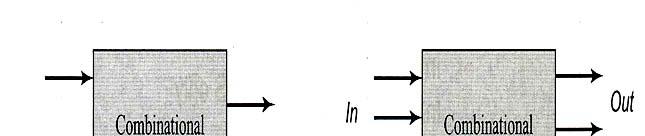
 igital Integrated Circuits esign Perspective esigning Combinational Logic Circuits 1 Combinational vs. Sequential Logic In Combinational Logic Circuit Out In Combinational Logic Circuit Out State Combinational
EECS 141 F01 Lecture 17
 EECS 4 F0 Lecture 7 With major inputs/improvements From Mary-Jane Irwin (Penn State) Dynamic CMOS In static circuits at every point in time (except when switching) the output is connected to either GND
Digital Integrated Circuits A Design Perspective
 Digital Integrated Circuits Design Perspective Designing Combinational Logic Circuits Fuyuzhuo School of Microelectronics,SJTU Introduction Digital IC Dynamic Logic Introduction Digital IC 2 EE141 Dynamic
COMP 103. Lecture 16. Dynamic Logic
 COMP 03 Lecture 6 Dynamic Logic Reading: 6.3, 6.4 [ll lecture notes are adapted from Mary Jane Irwin, Penn State, which were adapted from Rabaey s Digital Integrated Circuits, 2002, J. Rabaey et al.] COMP03
Digital Integrated Circuits Designing Combinational Logic Circuits. Fuyuzhuo
 Digital Integrated Circuits Designing Combinational Logic Circuits Fuyuzhuo Introduction Digital IC Dynamic Logic Introduction Digital IC EE141 2 Dynamic logic outline Dynamic logic principle Dynamic logic
Pass-Transistor Logic
 -all 26 Digital tegrated ircuits nnouncements No new homework this week roject phase one due on Monday Midterm 2 next Thursday Review session on Tuesday Lecture 8 Logic Dynamic Logic EE4 EE4 2 lass Material
Integrated Circuits & Systems
 Federal University of Santa Catarina Center for Technology Computer Science & Electronics Engineering Integrated Circuits & Systems INE 5442 Lecture 16 CMOS Combinational Circuits - 2 guntzel@inf.ufsc.br
CMPEN 411 VLSI Digital Circuits Spring 2011 Lecture 07: Pass Transistor Logic
 CMPEN 411 VLSI Digital Circuits Spring 2011 Lecture 07: Pass Transistor Logic [dapted from Rabaey s Digital Integrated Circuits, Second Edition, 2003 J. Rabaey,. Chandrakasan,. Nikolic] Sp11 CMPEN 411
Topics. Dynamic CMOS Sequential Design Memory and Control. John A. Chandy Dept. of Electrical and Computer Engineering University of Connecticut
 Topics Dynamic CMOS Sequential Design Memory and Control Dynamic CMOS In static circuits at every point in time (except when switching) the output is connected to either GND or V DD via a low resistance
Miscellaneous Lecture topics. Mary Jane Irwin [Adapted from Rabaey s Digital Integrated Circuits, 2002, J. Rabaey et al.]
![Miscellaneous Lecture topics. Mary Jane Irwin [Adapted from Rabaey s Digital Integrated Circuits, 2002, J. Rabaey et al.]](/thumbs/81/84503671.jpg "Miscellaneous Lecture topics. Mary Jane Irwin [Adapted from Rabaey s Digital Integrated Circuits, 2002, J. Rabaey et al.]") Miscellaneous Lecture topics Mary Jane Irwin [dapted from Rabaey s Digital Integrated Circuits, 2002, J. Rabaey et al.] MOS Switches MOS transistors can be viewed as simple switches. In an N-Switch, the
Miscellaneous Lecture topics Mary Jane Irwin [dapted from Rabaey s Digital Integrated Circuits, 2002, J. Rabaey et al.] MOS Switches MOS transistors can be viewed as simple switches. In an N-Switch, the
ΗΜΥ 307 ΨΗΦΙΑΚΑ ΟΛΟΚΛΗΡΩΜΕΝΑ ΚΥΚΛΩΜΑΤΑ Εαρινό Εξάμηνο 2018
 ΗΜΥ 307 ΨΗΦΙΑΚΑ ΟΛΟΚΛΗΡΩΜΕΝΑ ΚΥΚΛΩΜΑΤΑ Εαρινό Εξάμηνο 2018 ΔΙΑΛΕΞΗ 11: Dynamic CMOS Circuits ΧΑΡΗΣ ΘΕΟΧΑΡΙΔΗΣ (ttheocharides@ucy.ac.cy) (ack: Prof. Mary Jane Irwin and Vijay Narayanan) [Προσαρμογή από
CMOS Digital Integrated Circuits Lec 10 Combinational CMOS Logic Circuits
 Lec 10 Combinational CMOS Logic Circuits 1 Combinational vs. Sequential Logic In Combinational Logic circuit Out In Combinational Logic circuit Out State Combinational The output is determined only by
Based on slides/material by. Topic 3-4. Combinational Logic. Outline. The CMOS Inverter: A First Glance
 ased on slides/material by Topic 3 J. Rabaey http://bwrc.eecs.berkeley.edu/lasses/icook/instructors.html Digital Integrated ircuits: Design Perspective, Prentice Hall D. Harris http://www.cmosvlsi.com/coursematerials.html
CMOS logic gates. João Canas Ferreira. March University of Porto Faculty of Engineering
 CMOS logic gates João Canas Ferreira University of Porto Faculty of Engineering March 2016 Topics 1 General structure 2 General properties 3 Cell layout João Canas Ferreira (FEUP) CMOS logic gates March
CPE/EE 427, CPE 527 VLSI Design I Pass Transistor Logic. Review: CMOS Circuit Styles
 PE/EE 427, PE 527 VLI Design I Pass Transistor Logic Department of Electrical and omputer Engineering University of labama in Huntsville leksandar Milenkovic ( www.ece.uah.edu/~milenka ) Review: MO ircuit
EEC 118 Lecture #6: CMOS Logic. Rajeevan Amirtharajah University of California, Davis Jeff Parkhurst Intel Corporation
 EEC 118 Lecture #6: CMOS Logic Rajeevan mirtharajah University of California, Davis Jeff Parkhurst Intel Corporation nnouncements Quiz 1 today! Lab 2 reports due this week Lab 3 this week HW 3 due this
CPE/EE 427, CPE 527 VLSI Design I L18: Circuit Families. Outline
 CPE/EE 47, CPE 57 VLI Design I L8: Circuit Families Department of Electrical and Computer Engineering University of labama in Huntsville leksandar Milenkovic ( www.ece.uah.edu/~milenka ) www.ece.uah.edu/~milenka/cpe57-05f
Static CMOS Circuits
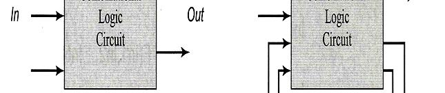
 Static MOS ircuits l onventional (ratio-less) static MOS» overed so far l Ratio-ed logic (depletion load, pseudo nmos) l ass transistor logic ombinational vs. Sequential Logic In Logic ircuit In Logic
EE 466/586 VLSI Design. Partha Pande School of EECS Washington State University
 EE 466/586 VLSI Design Partha Pande School of EECS Washington State University pande@eecs.wsu.edu Lecture 9 Propagation delay Power and delay Tradeoffs Follow board notes Propagation Delay Switching Time
Static CMOS Circuits. Example 1
 Static CMOS Circuits Conventional (ratio-less) static CMOS Covered so far Ratio-ed logic (depletion load, pseudo nmos) Pass transistor logic ECE 261 Krish Chakrabarty 1 Example 1 module mux(input s, d0,
EEC 116 Lecture #5: CMOS Logic. Rajeevan Amirtharajah Bevan Baas University of California, Davis Jeff Parkhurst Intel Corporation
 EEC 116 Lecture #5: CMOS Logic Rajeevan mirtharajah Bevan Baas University of California, Davis Jeff Parkhurst Intel Corporation nnouncements Quiz 1 today! Lab 2 reports due this week Lab 3 this week HW
CPE/EE 427, CPE 527 VLSI Design I Delay Estimation. Department of Electrical and Computer Engineering University of Alabama in Huntsville
 CPE/EE 47, CPE 57 VLSI Design I Delay Estimation Department of Electrical and Computer Engineering University of labama in Huntsville leksandar Milenkovic ( www.ece.uah.edu/~milenka ) Review: CMOS Circuit
Announcements. EE141-Spring 2007 Digital Integrated Circuits. CMOS SRAM Analysis (Read/Write) Class Material. Layout. Read Static Noise Margin
 Class Material. Layout. Read Static Noise Margin") Vo l ta ge ri s e [ V] EE-Spring 7 Digital Integrated ircuits Lecture SRM Project Launch nnouncements No new labs next week and week after Use labs to work on project Homework #6 due Fr. pm Project updated
Vo l ta ge ri s e [ V] EE-Spring 7 Digital Integrated ircuits Lecture SRM Project Launch nnouncements No new labs next week and week after Use labs to work on project Homework #6 due Fr. pm Project updated
CPE/EE 427, CPE 527 VLSI Design I L07: CMOS Logic Gates, Pass Transistor Logic. Review: CMOS Circuit Styles
 PE/EE 427, PE 527 VLI esign I L07: MO Logic Gates, Pass Transistor Logic epartment of Electrical and omputer Engineering University of labama in Huntsville leksandar Milenkovic ( www.ece.uah.edu/~milenka
5.0 CMOS Inverter. W.Kucewicz VLSICirciuit Design 1
 5.0 CMOS Inverter W.Kucewicz VLSICirciuit Design 1 Properties Switching Threshold Dynamic Behaviour Capacitance Propagation Delay nmos/pmos Ratio Power Consumption Contents W.Kucewicz VLSICirciuit Design
Dynamic Combinational Circuits. Dynamic Logic
 Dynamic Combinational Circuits Dynamic circuits Charge sharing, charge redistribution Domino logic np-cmos (zipper CMOS) Krish Chakrabarty 1 Dynamic Logic Dynamic gates use a clocked pmos pullup Two modes:
MOSFET and CMOS Gate. Copy Right by Wentai Liu
 MOSFET and CMOS Gate CMOS Inverter DC Analysis - Voltage Transfer Curve (VTC) Find (1) (2) (3) (4) (5) (6) V OH min, V V OL min, V V IH min, V V IL min, V OHmax OLmax IHmax ILmax NM L = V ILmax V OL max
Lecture 4: CMOS review & Dynamic Logic
 Lecture 4: CMOS review & Dynamic Logic Reading: ch5, ch6 Overview CMOS basics Power and energy in CMOS Dynamic logic 1 CMOS Properties Full rail-to-rail swing high noise margins Logic levels not dependent
THE INVERTER. Inverter
 THE INVERTER DIGITAL GATES Fundamental Parameters Functionality Reliability, Robustness Area Performance» Speed (delay)» Power Consumption» Energy Noise in Digital Integrated Circuits v(t) V DD i(t) (a)
B.Supmonchai August 1st, q In-depth discussion of CMOS logic families. q Optimizing gate metrics. q High Performance circuit-design techniques
 ugust st, 4 Goals of This hapter hapter 6 Static MOS ircuits oonchuay Supmonchai Integrated esign pplication Research (IR) Laboratory ugust, 4; Revised - June 8, 5 In-depth discussion of MOS logic families
MASSACHUSETTS INSTITUTE OF TECHNOLOGY Department of Electrical Engineering and Computer Sciences
 MSSCHUSETTS INSTITUTE OF TECHNOLOGY Department of Electrical Engineering and Computer Sciences nalysis and Design of Digital Integrated Circuits (6.374) - Fall 2003 Quiz #1 Prof. nantha Chandrakasan Student
The CMOS Inverter: A First Glance
 The CMOS Inverter: A First Glance V DD S D V in V out C L D S CMOS Inverter N Well V DD V DD PMOS 2λ PMOS Contacts In Out In Out Metal 1 NMOS Polysilicon NMOS GND CMOS Inverter: Steady State Response V
CHAPTER 15 CMOS DIGITAL LOGIC CIRCUITS
 CHAPTER 5 CMOS DIGITAL LOGIC CIRCUITS Chapter Outline 5. CMOS Logic Gate Circuits 5. Digital Logic Inverters 5.3 The CMOS Inverter 5.4 Dynamic Operation of the CMOS Inverter 5.5 Transistor Sizing 5.6 Power
Power Dissipation. Where Does Power Go in CMOS?
 Power Dissipation [Adapted from Chapter 5 of Digital Integrated Circuits, 2003, J. Rabaey et al.] Where Does Power Go in CMOS? Dynamic Power Consumption Charging and Discharging Capacitors Short Circuit
CPE/EE 427, CPE 527 VLSI Design I L06: CMOS Inverter, CMOS Logic Gates. Course Administration. CMOS Inverter: A First Look
 CPE/EE 47, CPE 57 VLSI esign I L6: CMOS Inverter, CMOS Logic Gates epartment of Electrical and Computer Engineering University of labama in Huntsville leksandar Milenkovic ( www.ece.uah.edu/~milenka )
Digital Integrated Circuits 2nd Inverter
 Digital Integrated Circuits The Inverter The CMOS Inverter V DD Analysis Inverter complex gate Cost V in V out complexity & Area Integrity and robustness C L Static behavior Performance Dynamic response
Lecture 6: Circuit design part 1
 Lecture 6: Circuit design part 6. Combinational circuit design 6. Sequential circuit design 6.3 Circuit simulation 6.4. Hardware description language Combinational Circuit Design. Combinational circuit
Dynamic Combinational Circuits. Dynamic Logic
 Dynamic Combinational Circuits Dynamic circuits Charge sharing, charge redistribution Domino logic np-cmos (zipper CMOS) Krish Chakrabarty 1 Dynamic Logic Dynamic gates use a clocked pmos pullup Two modes:
ENEE 359a Digital VLSI Design
 SLIDE 1 ENEE 359a Digital VLSI Design Prof. blj@eng.umd.edu Credit where credit is due: Slides contain original artwork ( Jacob 2004) as well as material taken liberally from Irwin & Vijay s CSE477 slides
EEE 421 VLSI Circuits
 EEE 421 CMOS Properties Full rail-to-rail swing high noise margins» Logic levels not dependent upon the relative device sizes transistors can be minimum size ratioless Always a path to V dd or GND in steady
The CMOS Inverter: A First Glance
 The CMOS Inverter: A First Glance V DD V in V out C L CMOS Properties Full rail-to-rail swing Symmetrical VTC Propagation delay function of load capacitance and resistance of transistors No static power
Interconnect (2) Buffering Techniques. Logical Effort
 Buffering Techniques. Logical Effort") Interconnect (2) Buffering Techniques. Logical Effort Lecture 14 18-322 Fall 2002 Textbook: [Sections 4.2.1, 8.2.3] A few announcements! M1 is almost over: The check-off is due today (by 9:30PM) Students
Interconnect (2) Buffering Techniques. Logical Effort Lecture 14 18-322 Fall 2002 Textbook: [Sections 4.2.1, 8.2.3] A few announcements! M1 is almost over: The check-off is due today (by 9:30PM) Students
CARNEGIE MELLON UNIVERSITY DEPARTMENT OF ELECTRICAL AND COMPUTER ENGINEERING DIGITAL INTEGRATED CIRCUITS FALL 2002
 CARNEGIE MELLON UNIVERSITY DEPARTMENT OF ELECTRICAL AND COMPUTER ENGINEERING 18-322 DIGITAL INTEGRATED CIRCUITS FALL 2002 Final Examination, Monday Dec. 16, 2002 NAME: SECTION: Time: 180 minutes Closed
ESE 570: Digital Integrated Circuits and VLSI Fundamentals
 ESE 570: Digital Integrated Circuits and VLSI Fundamentals Lec 18: March 27, 2018 Dynamic Logic, Charge Injection Lecture Outline! Sequential MOS Logic " D-Latch " Timing Constraints! Dynamic Logic " Domino
CMOS Inverter (static view)
") Review: Design Abstraction Levels SYSTEM CMOS Inverter (static view) + MODULE GATE [Adapted from Chapter 5. 5.3 CIRCUIT of G DEVICE Rabaey s Digital Integrated Circuits,, J. Rabaey et al.] S D Review:
Review: Design Abstraction Levels SYSTEM CMOS Inverter (static view) + MODULE GATE [Adapted from Chapter 5. 5.3 CIRCUIT of G DEVICE Rabaey s Digital Integrated Circuits,, J. Rabaey et al.] S D Review:
Logical Effort: Designing for Speed on the Back of an Envelope David Harris Harvey Mudd College Claremont, CA
 Logical Effort: Designing for Speed on the Back of an Envelope David Harris David_Harris@hmc.edu Harvey Mudd College Claremont, CA Outline o Introduction o Delay in a Logic Gate o Multi-stage Logic Networks
ECE 546 Lecture 10 MOS Transistors
 ECE 546 Lecture 10 MOS Transistors Spring 2018 Jose E. Schutt-Aine Electrical & Computer Engineering University of Illinois jesa@illinois.edu NMOS Transistor NMOS Transistor N-Channel MOSFET Built on p-type
CMOS Inverter: CPE/EE 427, CPE 527 VLSI Design I L06: CMOS Inverter, CMOS Logic Gates. Course Administration. CMOS Properties.
 CMOS Inverter: Steady State Response CPE/EE 47, CPE 57 VLSI esign I L6: CMOS Inverter, CMOS Logic Gates R p V OL = V OH = V M = f(r n, R p ) epartment of Electrical and Computer Engineering University
CMPEN 411 VLSI Digital Circuits. Lecture 04: CMOS Inverter (static view)
") CMPEN 411 VLSI Digital Circuits Lecture 04: CMOS Inverter (static view) Kyusun Choi [Adapted from Rabaey s Digital Integrated Circuits, Second Edition, 2003 J. Rabaey, A. Chandrakasan, B. Nikolic] CMPEN
CMPEN 411 VLSI Digital Circuits Lecture 04: CMOS Inverter (static view) Kyusun Choi [Adapted from Rabaey s Digital Integrated Circuits, Second Edition, 2003 J. Rabaey, A. Chandrakasan, B. Nikolic] CMPEN
Lecture 14: Circuit Families
 Introduction to CMOS VLSI Design Lecture 4: Circuit Families David Harris, Harvey Mudd College Kartik Mohanram and Steven Levitan University of Pittsburgh Outline q Pseudo-nMOS Logic q Dynamic Logic q
ECE 438: Digital Integrated Circuits Assignment #4 Solution The Inverter
 ECE 438: Digital Integrated Circuits Assignment #4 The Inverter Text: Chapter 5, Digital Integrated Circuits 2 nd Ed, Rabaey 1) Consider the CMOS inverter circuit in Figure P1 with the following parameters.
Dynamic operation 20
 Dynamic operation 20 A simple model for the propagation delay Symmetric inverter (rise and fall delays are identical) otal capacitance is linear t p Minimum length devices R W C L t = 0.69R C = p W L 0.69
Hw 6 due Thursday, Nov 3, 5pm No lab this week
 EE141 Fall 2005 Lecture 18 dders nnouncements Hw 6 due Thursday, Nov 3, 5pm No lab this week Midterm 2 Review: Tue Nov 8, North Gate Hall, Room 105, 6:30-8:30pm Exam: Thu Nov 10, Morgan, Room 101, 6:30-8:00pm
ECE 342 Solid State Devices & Circuits 4. CMOS
 ECE 34 Solid State Devices & Circuits 4. CMOS Jose E. Schutt-Aine Electrical & Computer Engineering University of Illinois jschutt@emlab.uiuc.edu ECE 34 Jose Schutt Aine 1 Digital Circuits V IH : Input
2007 Fall: Electronic Circuits 2 CHAPTER 10. Deog-Kyoon Jeong School of Electrical Engineering
 007 Fall: Electronic Circuits CHAPTER 10 Digital CMOS Logic Circuits Deog-Kyoon Jeong dkjeong@snu.ac.kr k School of Electrical Engineering Seoul lnational luniversity it Introduction In this chapter, we
Lecture 8: Combinational Circuit Design
 Lecture 8: Combinational Circuit Design Mark McDermott Electrical and Computer Engineering The University of Texas at ustin 9/5/8 Verilog to Gates module mux(input s, d0, d, output y); assign y = s? d
Topics to be Covered. capacitance inductance transmission lines
 Topics to be Covered Circuit Elements Switching Characteristics Power Dissipation Conductor Sizes Charge Sharing Design Margins Yield resistance capacitance inductance transmission lines Resistance of
Digital Integrated Circuits A Design Perspective
 Digital Integrated Circuits A Design Perspective Jan M. Rabaey Anantha Chandrakasan Borivoje Nikolic Designing Sequential Logic Circuits November 2002 Sequential Logic Inputs Current State COMBINATIONAL
Spiral 2 7. Capacitance, Delay and Sizing. Mark Redekopp
 2-7.1 Spiral 2 7 Capacitance, Delay and Sizing Mark Redekopp 2-7.2 Learning Outcomes I understand the sources of capacitance in CMOS circuits I understand how delay scales with resistance, capacitance
VLSI Design, Fall Logical Effort. Jacob Abraham
 6. Logical Effort 6. Logical Effort Jacob Abraham Department of Electrical and Computer Engineering The University of Texas at Austin VLSI Design Fall 207 September 20, 207 ECE Department, University of
EECS 141: FALL 05 MIDTERM 1
 University of California College of Engineering Department of Electrical Engineering and Computer Sciences D. Markovic TuTh 11-1:3 Thursday, October 6, 6:3-8:pm EECS 141: FALL 5 MIDTERM 1 NAME Last SOLUTION
Lecture 5: DC & Transient Response
 Lecture 5: DC & Transient Response Outline q Pass Transistors q DC Response q Logic Levels and Noise Margins q Transient Response q RC Delay Models q Delay Estimation 2 Activity 1) If the width of a transistor
MODULE 5 Chapter 7. Clocked Storage Elements
 MODULE 5 Chapter 7 Clocked Storage Elements 3/9/2015 1 Outline Background Clocked Storage Elements Timing, terminology, classification Static CSEs Latches Registers Dynamic CSEs Latches Registers 3/9/2015
ENGR890 Digital VLSI Design Fall Lecture 4: CMOS Inverter (static view)
") ENGR89 Digital VLSI Design Fall 5 Lecture 4: CMOS Inverter (static view) [Adapted from Chapter 5 of Digital Integrated Circuits, 3, J. Rabaey et al.] [Also borrowed from Vijay Narayanan and Mary Jane Irwin]
ENGR89 Digital VLSI Design Fall 5 Lecture 4: CMOS Inverter (static view) [Adapted from Chapter 5 of Digital Integrated Circuits, 3, J. Rabaey et al.] [Also borrowed from Vijay Narayanan and Mary Jane Irwin]
Very Large Scale Integration (VLSI)
") Very Large Scale Integration (VLSI) Lecture 4 Dr. Ahmed H. Madian Ah_madian@hotmail.com Dr. Ahmed H. Madian-VLSI Contents Delay estimation Simple RC model Penfield-Rubenstein Model Logical effort Delay
Very Large Scale Integration (VLSI) Lecture 4 Dr. Ahmed H. Madian Ah_madian@hotmail.com Dr. Ahmed H. Madian-VLSI Contents Delay estimation Simple RC model Penfield-Rubenstein Model Logical effort Delay
Integrated Circuits & Systems
 Federal University of Santa Catarina Center for Technology Computer Science & Electronics Engineering Integrated Circuits & Systems INE 5442 Lecture 14 The CMOS Inverter: dynamic behavior (sizing, inverter
EE213, Spr 2017 HW#3 Due: May 17 th, in class. Figure 1
 RULES: Please try to work on your own. Discussion is permissible, but identical submissions are unacceptable! Please show all intermediate steps: a correct solution without an explanation will get zero
Chapter 5. The Inverter. V1. April 10, 03 V1.1 April 25, 03 V2.1 Nov Inverter
 Chapter 5 The Inverter V1. April 10, 03 V1.1 April 25, 03 V2.1 Nov.12 03 Objective of This Chapter Use Inverter to know basic CMOS Circuits Operations Watch for performance Index such as Speed (Delay calculation)
EECS 427 Lecture 8: Adders Readings: EECS 427 F09 Lecture 8 1. Reminders. HW3 project initial proposal: due Wednesday 10/7
 EECS 427 Lecture 8: dders Readings: 11.1-11.3.3 3 EECS 427 F09 Lecture 8 1 Reminders HW3 project initial proposal: due Wednesday 10/7 You can schedule a half-hour hour appointment with me to discuss your
CMOS INVERTER. Last Lecture. Metrics for qualifying digital circuits. »Cost» Reliability» Speed (delay)»performance
»performance") CMOS INVERTER Last Lecture Metrics for qualifying digital circuits»cost» Reliability» Speed (delay)»performance 1 Today s lecture The CMOS inverter at a glance An MOS transistor model for manual analysis
CMOS INVERTER Last Lecture Metrics for qualifying digital circuits»cost» Reliability» Speed (delay)»performance 1 Today s lecture The CMOS inverter at a glance An MOS transistor model for manual analysis
MODULE III PHYSICAL DESIGN ISSUES
 VLSI Digital Design MODULE III PHYSICAL DESIGN ISSUES 3.2 Power-supply and clock distribution EE - VDD -P2006 3:1 3.1.1 Power dissipation in CMOS gates Power dissipation importance Package Cost. Power
and V DS V GS V T (the saturation region) I DS = k 2 (V GS V T )2 (1+ V DS )
 I DS = k 2 (V GS V T )2 (1+ V DS )") ECE 4420 Spring 2005 Page 1 FINAL EXAMINATION NAME SCORE /100 Problem 1O 2 3 4 5 6 7 Sum Points INSTRUCTIONS: This exam is closed book. You are permitted four sheets of notes (three of which are your sheets
ECE 4420 Spring 2005 Page 1 FINAL EXAMINATION NAME SCORE /100 Problem 1O 2 3 4 5 6 7 Sum Points INSTRUCTIONS: This exam is closed book. You are permitted four sheets of notes (three of which are your sheets
Lecture 6: DC & Transient Response
 Lecture 6: DC & Transient Response Slides courtesy of Deming Chen Slides based on the initial set from David Harris CMOS VLSI Design Outline Pass Transistors DC Response Logic Levels and Noise Margins
9/18/2008 GMU, ECE 680 Physical VLSI Design
 ECE680: Physical VLSI esign Chapter IV esigning Sequential Logic Circuits (Chapter 7) 1 Sequential Logic Inputs Current State COMBINATIONAL LOGIC Registers Outputs Next state 2 storage mechanisms positive
Lecture Outline. ESE 570: Digital Integrated Circuits and VLSI Fundamentals. Review: 1st Order RC Delay Models. Review: Two-Input NOR Gate (NOR2)
") ESE 570: Digital Integrated Circuits and VLSI Fundamentals Lec 14: March 1, 2016 Combination Logic: Ratioed and Pass Logic Lecture Outline! CMOS Gates Review " CMOS Worst Case Analysis! Ratioed Logic Gates!
ESE 570: Digital Integrated Circuits and VLSI Fundamentals Lec 14: March 1, 2016 Combination Logic: Ratioed and Pass Logic Lecture Outline! CMOS Gates Review " CMOS Worst Case Analysis! Ratioed Logic Gates!
DC and Transient Responses (i.e. delay) (some comments on power too!)
 (some comments on power too!)") DC and Transient Responses (i.e. delay) (some comments on power too!) Michael Niemier (Some slides based on lecture notes by David Harris) 1 Lecture 02 - CMOS Transistor Theory & the Effects of Scaling
DC and Transient Responses (i.e. delay) (some comments on power too!) Michael Niemier (Some slides based on lecture notes by David Harris) 1 Lecture 02 - CMOS Transistor Theory & the Effects of Scaling
GMU, ECE 680 Physical VLSI Design
 ECE680: Physical VLSI esign Chapter IV esigning Sequential Logic Circuits (Chapter 7) 1 Sequential Logic Inputs Current State COMBINATIONAL LOGIC Registers Outputs Next state 2 storage mechanisms positive
EE 466/586 VLSI Design. Partha Pande School of EECS Washington State University
 EE 466/586 VLSI Design Partha Pande School of EECS Washington State University pande@eecs.wsu.edu Lecture 8 Power Dissipation in CMOS Gates Power in CMOS gates Dynamic Power Capacitance switching Crowbar
Logic Gate Sizing. The method of logical effort. João Canas Ferreira. March University of Porto Faculty of Engineering
 Logic Gate Sizing The method of logical effort João Canas Ferreira University of Porto Faculty of Engineering March 016 Topics 1 Modeling CMOS Gates Chain of logic gates João Canas Ferreira (FEUP) Logic
Announcements. EE141- Spring 2003 Lecture 8. Power Inverter Chain
 - Spring 2003 Lecture 8 Power Inverter Chain Announcements Homework 3 due today. Homework 4 will be posted later today. Special office hours from :30-3pm at BWRC (in lieu of Tuesday) Today s lecture Power
VLSI Design I; A. Milenkovic 1
 ourse dministration PE/EE 47, PE 57 VLI esign I L6: omplementary MO Logic Gates epartment of Electrical and omputer Engineering University of labama in Huntsville leksandar Milenkovic ( www.ece.uah.edu/~milenka
EE241 - Spring 2000 Advanced Digital Integrated Circuits. Announcements
 EE241 - Spring 2000 Advanced Digital Integrated Circuits Lecture 3 Circuit Optimization for Speed Announcements Tu 2/8/00 class will be pre-taped on Friday, 2/4, 4-5:30 203 McLaughlin Class notes are available
VLSI Design I; A. Milenkovic 1
 PE/EE 47, PE 57 VLI esign I L6: tatic MO Logic epartment of Electrical and omputer Engineering University of labama in Huntsville leksandar Milenkovic ( www. ece.uah.edu/~milenka ) www. ece.uah.edu/~milenka/cpe57-3f
C.K. Ken Yang UCLA Courtesy of MAH EE 215B
 Decoders: Logical Effort Applied C.K. Ken Yang UCLA yang@ee.ucla.edu Courtesy of MAH 1 Overview Reading Rabaey 6.2.2 (Ratio-ed logic) W&H 6.2.2 Overview We have now gone through the basics of decoders,
Digital Microelectronic Circuits ( ) The CMOS Inverter. Lecture 4: Presented by: Adam Teman
 The CMOS Inverter. Lecture 4: Presented by: Adam Teman") Digital Microelectronic Circuits (361-1-301 ) Presented by: Adam Teman Lecture 4: The CMOS Inverter 1 Last Lectures Moore s Law Terminology» Static Properties» Dynamic Properties» Power The MOSFET Transistor»
Digital Microelectronic Circuits (361-1-301 ) Presented by: Adam Teman Lecture 4: The CMOS Inverter 1 Last Lectures Moore s Law Terminology» Static Properties» Dynamic Properties» Power The MOSFET Transistor»
EE5311- Digital IC Design
 EE5311- Digital IC Design Module 3 - The Inverter Janakiraman V Assistant Professor Department of Electrical Engineering Indian Institute of Technology Madras Chennai September 6, 2017 Janakiraman, IITM
CMOS Digital Integrated Circuits Lec 13 Semiconductor Memories
 Lec 13 Semiconductor Memories 1 Semiconductor Memory Types Semiconductor Memories Read/Write (R/W) Memory or Random Access Memory (RAM) Read-Only Memory (ROM) Dynamic RAM (DRAM) Static RAM (SRAM) 1. Mask
EE141-Fall 2012 Digital Integrated Circuits. Announcements. Homework #3 due today. Homework #4 due next Thursday EECS141 EE141
 EE4-Fall 0 Digital Integrated Circuits Lecture 7 Gate Delay and Logical Effort nnouncements Homework #3 due today Homework #4 due next Thursday Class Material Last lecture Inverter delay optimization Today
Midterm. ESE 570: Digital Integrated Circuits and VLSI Fundamentals. Lecture Outline. Pass Transistor Logic. Restore Output.
 ESE 570: Digital Integrated Circuits and VLSI Fundamentals Lec 16: March 21, 2017 Transmission Gates, Euler Paths, Energy Basics Review Midterm! Midterm " Mean: 79.5 " Standard Dev: 14.5 2 Lecture Outline!
ESE 570: Digital Integrated Circuits and VLSI Fundamentals
 ESE 570: Digital Integrated Circuits and VLSI Fundamentals Lec 19: March 29, 2018 Memory Overview, Memory Core Cells Today! Charge Leakage/Charge Sharing " Domino Logic Design Considerations! Logic Comparisons!
Logical Effort. Sizing Transistors for Speed. Estimating Delays
 Logical Effort Sizing Transistors for Speed Estimating Delays Would be nice to have a back of the envelope method for sizing gates for speed Logical Effort Book by Sutherland, Sproull, Harris Chapter 1
EE241 - Spring 2000 Advanced Digital Integrated Circuits. Announcements
 EE241 - Spring 2 Advanced Digital Integrated Circuits Lecture 11 Low Power-Low Energy Circuit Design Announcements Homework #2 due Friday, 3/3 by 5pm Midterm project reports due in two weeks - 3/7 by 5pm