SMG2305L. P-Channel Enhancement Mode Power Mos.FET WILLAS ELECTRONIC CORP. Description. Features. Applications. Absolute Maximum Ratings
|
|
|
- Helena Robbins
- 5 years ago
- Views:
Transcription

1 P-Channel Enhancement Mde Pwer Ms.FET Descriptin The prvide the designer with the best cmbinatin f fast switching, lw n-resistance and cst-effectiveness. The is universally preferred fr all cmmercial industrial surface munt applicatin and suited fr lw vltage applicatins such as DC/DC cnverters. Features S L Tp iew 1 G B D C J SC-59 Dim Min Max B C D G H J * Super high dense cell design fr extremely lw RDS(ON) * Reliable and rugged pplicatins H Gate Drain Surce K D K L S ll Dimensin in mm * Pwer Management in Ntebk Cmputer * Prtable Equipment * Battery Pwered System G Marking : 05 S bslute Maximum Ratings Parameter Symbl Ratings Unit Drain-Surce ltage DS -0 Gate-Surce ltage GS ±1 Cntinuus Drain Current ID@T=5 C -4. Cntinuus Drain Current ID@T=70 C -.4 Pulsed Drain Current IDM -10 Ttal Pwer Dissipatin PD@T=5 C 1.8 W Linear Derating Factr 0.01 W / C Operating Junctin and Strage Temperature Range Tj, Tstg -55~+150 C Thermal Data Parameter Symbl Ratings Unit Thermal Resistance Junctin-ambient Rthj-a 90 C /W
2 P-Channel Enhancement Mde Pwer Ms.FET Electrical Characteristics( Tj=5 C Unless therwise specified) Parameter Symbl Min. Typ. Max. Unit Test Cnditin Drain-Surce Breakdwn ltage BDSS -0 GS=0, ID=-50u Breakdwn ltage Temp. Cefficient BDS/ Tj -0.1 / Reference t 5 C,ID=-1m Gate Threshld ltage GS(th) -0.5 DS=GS, ID=-50u Gate-Surce Leakage Current IGSS ± 100 n GS= ±1 Drain-Surce Leakage Current (Tj=5 C) Drain-Surce Leakage Current (Tj=70 C) IDSS u u DS=-0,GS=0 DS=-16,GS=0 0 5 GS=-4.5, ID=-4.0 Static Drain-Surce On-Resistance RDS(ON) 6 4 GS=-.5, ID=-4.0 m GS=-1.8, ID=- 60 GS=-1.5, ID=-1 Ttal Gate Charge Gate-Surce Charge Gate-Drain ("Miller") Charge Qg Qgs Qgd nc ID=-4. DS=-16 GS=-4.5 Turn-n Delay Time Rise Time Turn-ff Delay Time Fall Time Td(ON) Tr Td(Off) Tf ns DS=-15 ID=-4. GS=-10 RG=6 RD=.6 Input Capacitance Output Capacitance Reverse Transfer Capacitance Ciss Css Crss pf GS=0 DS=-15 f=1.0mhz Frward Transcnductance Gfs 9 S DS=-5, ID=-.8 Surce-Drain Dide Parameter Symbl Min. Typ. Max. Unit Test Cnditin Frward On ltage SD -1. IS=-1., GS=0. Reverse Recvery Time Trr Reverse Recvery Charge Qrr nc 7.7 ns Is=-4.,GS=0 dl/dt=100/us Ntes: 1.Pulse width limited by Max. junctin temperature..pulse width 00us, dutycycle %..Surface munted n 1 inch cpper pad f FR4 bard; 70 C/W when munted n min. cpper pad.

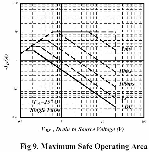
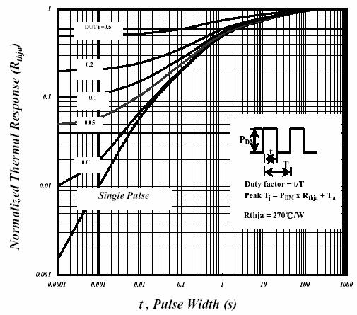
3 P-Channel Enhancement Mde Pwer Ms.FET Characteristics Curve
4 P-Channel Enhancement Mde Pwer Ms.FET
5 P-Channel Enhancement Mde Pwer Ms.FET Ordering Infrmatin: Device PN Packing T (1) G () WS Tape&Reel: Kpcs/Reel Nte: (1) Packing cde, Tape & Reel () RHS prduct fr packing cde suffix G ;Halgen free prduct fr packing cde suffix H ***Disclaimer*** WILLS reserves the right t make changes withut ntice t any prduct specificatin herein, t make crrectins, mdificatins, enhancements r ther changes. WILLS r anyne n its behalf assumes n respnsibility r liability fr any errrs r inaccuracies. Data sheet specificatins and its infrmatin cntained are intended t prvide a prduct descriptin nly. "Typical" parameters which may be included n WILLS data sheets and/ r specificatins can and d vary in different applicatins and actual perfrmance may vary ver time. WILLS des nt assume any liability arising ut f the applicatin r use f any prduct r circuit. WILLS prducts are nt designed, intended r authrized fr use in medical, life saving implant r ther applicatins intended fr life sustaining r ther related applicatins where a failure r malfunctin f cmpnent r circuitry may directly r indirectly cause injury r threaten a life withut expressed written apprval f WILLS. Custmers using r selling WILLS cmpnents fr use in such applicatins d s at their wn risk and shall agree t fully indemnify WILLS Inc and its subsidiaries harmless against all claims, damages and expenditures.
SINGLE-PHASE GLASS PASSIVATED SILICON BRIDGE RECTIFIER. VOLTAGE RANGE 50 to 1000 Volts CURRENT 10 Amperes VRRM VRMS VDC IFSM
 SINGLE-PHASE GLASS PASSIVATED SILICON BRIDGE RECTIFIER VOLTAGE RANGE 5 t CURRENT Amperes RSM THRU RS7M FEATURES * Lw leakage * Lw frward vltage * Munting psitin : Any * Surge verlad rating: Amperes peak
N-Channel ENHANCEMENT MODE POWER MOSFET 0V
 PRIMARY CHARACTERISTICS BVD DSS 0V PR-PAK PACKAGE R DS(ON) I D. mω A FEATURES Low On-Resistance Low Input Capacitance Green Device Available Low Miller Charge 100% EAS and 100% Rg Guaranteed DESCRIPTION
List... Package outline... Features Mechanical data... Maximum ratings... Rating and characteristic curves... Pinning information...
 List List... Package utline... 1 2 Features... 2 Mechanical data... Maximum ratings... Rating and characteristic curves... 2 2~3 4 Pinning infrmatin... 5 Marking... Suggested slder pad layut... 5 5 Packing
DISCRETE SEMICONDUCTORS DATA SHEET. BF996S N-channel dual-gate MOS-FET. Product specification File under Discrete Semiconductors, SC07
 DISCRETE SEMICONDUCTORS DATA SHEET File under Discrete Semicnductrs, SC7 April 1991 FEATURES Prtected against excessive input vltage surges by integrated back-t-back dides between gates and surce. DESCRIPTION
Description Absolute Maximum Ratings Parameter Max. Units Thermal Resistance Parameter Typ. Max. Units
 l l l l l Advanced Prcess Technlgy Dynamic dv/dt Rating 175 C Operating Temperature Fast Switching Fully Avalanche Rated Descriptin Fifth Generatin HEXFETs frm Internatinal Rectifier utilize advanced prcessing
Description Absolute Maximum Ratings Parameter Max. Units Thermal Resistance Parameter Typ. Max. Units
 l Advanced Prcess Technlgy l Dynamic dv/dt Rating l 175 C Operating Temperature l Fast Switching l Fully Avalanche Rated l Lead-Free Descriptin Fifth Generatin HEXFETs frm Internatinal Rectifier utilize
C Soldering Temperature, for 10 seconds 300 (1.6mm from case )
") l l l l l l Advanced Prcess Technlgy Dynamic dv/dt Rating 175 C Operating Temperature Fast Switching Fully Avalanche Rated Lead-Free Descriptin Fifth Generatin HEXFET Pwer MOSFETs frm Internatinal Rectifier
l l l l l l Advanced Prcess Technlgy Dynamic dv/dt Rating 175 C Operating Temperature Fast Switching Fully Avalanche Rated Lead-Free Descriptin Fifth Generatin HEXFET Pwer MOSFETs frm Internatinal Rectifier
SSM9435. P-Channel Enhancement Mode MOSFET FEATURES. Product Summary SO-8. ABSOLUTE MAXIMUM RATINGS (TA = 25 C unless otherwise noted)
") Phnnel Enhncement Mde MOSFET Prduct Summry SO DS () ID () RDS(ON) (mω) Mx 7. @GS = 9 @GS =. D (,, 7, ) FETURES Super high density cell design fr lw RDS(ON). Rugged nd relible. SO pckge. Pb free. G () S(,,
Phnnel Enhncement Mde MOSFET Prduct Summry SO DS () ID () RDS(ON) (mω) Mx 7. @GS = 9 @GS =. D (,, 7, ) FETURES Super high density cell design fr lw RDS(ON). Rugged nd relible. SO pckge. Pb free. G () S(,,
List... Package outline... Features Mechanical data... Maximum ratings... Electrical characteristics... Rating and characteristic curves...
 List List... Package utline... 1 2 Features... 2 Mechanical data... Maximum ratings... Electrical characteristics... Rating and characteristic curves... 2 2 3 4 Pinning infrmatin... 5 Marking... Suggested
BF908; BF908R IMPORTANT NOTICE. use
 Rev. 3 14 Nvember 27 Prduct data sheet IMPORTANT NOTICE Dear custmer, As frm Octber 1st, 26 Philips Semicnductrs has a new trade name - NXP Semicnductrs, which will be used in future data sheets tgether
T0521SB. Applications. Features. Mechanical Characteristics. Circuit Diagram I/O_1. Description. Pin Configuration
 Features Transient prtectin fr high-speed data lines IEC 61000-4-2 (ESD) ±25kV (Air) ±20kV (Cntact) IEC 61000-4-2 (EFT)40A(5/50 ns) Cable Discharge Event (CDE) Package ptimized fr high-speed lines Ultra-small
400V N-Channel MOSFET GENERAL DESCRIPTION VDSS RDS(ON) ID. Features. Ordering Information 400V 0.55Ω 10.5A. This Power MOSFET is produced using
 ID. Features. Ordering Information 400V 0.55Ω 10.5A. This Power MOSFET is produced using") 400V N-Channel MOSFET GENERAL DESCRIPTION This Power MOSFET is produced using advanced planar stripe DMOS technology. This advanced technology has been especially tailored to minimize on-state resistance,
400V N-Channel MOSFET GENERAL DESCRIPTION This Power MOSFET is produced using advanced planar stripe DMOS technology. This advanced technology has been especially tailored to minimize on-state resistance,
List... Package outline... Features Mechanical data... Maximum ratings... Electrical characteristics... 3~4
 List List... Package utline... 1 2 Features... 2 Mechanical data... Maximum ratings... 2 2 Electrical characteristics... 3~4 Switching time equivalent test circuits... Rating and characteristic curves...
List... Package outline... Features Mechanical data... Maximum ratings and Electrical characteristics Rating and characteristic curves...
 Frmsa MS List List... Package utline... 1 2 Features... 2 Mechanical data... 2 Maximum ratings and Electrical characteristics... 2 Rating and characteristic curves... 3 Pinning infrmatin... 4 Marking...
List... Package outline... Features Mechanical data... Maximum ratings... Rating and characteristic curves... Pinning information...
 SMD Switching Dide V9WS THRU VWS rmsa MS List List... Package utline... eatures... Mechanical data... Maximum ratings... Rating and characteristic curves... 3 Pinning infrmatin... 4 Marking... Suggested
List... Package outline... Features Mechanical data... Maximum ratings... Switching time equivalent test circuits...
 SMD NPN Transistr Frmsa MS List List... Package utline... 1 2 Features... 2 Mechanical data... Maximum ratings... Switching time equivalent test circuits... Rating and characteristic curves... 2 2~3 4
Photocoupler Product Data Sheet LTV (M, S, S-TA, S-TA1, S-TP) Series Spec No.: DS Effective Date: 06/28/2011 LITE-ON DCC
 Series Spec No.: DS Effective Date: 06/28/2011 LITE-ON DCC") Phtcupler Prduct Data Sheet LTV-814 824 844 (M, S, S-TA, S-TA1, S-TP) Series Spec N.: DS-7-96-13 Effective Date: 6/28/211 Revisin: F LITE-ON DCC RELEASE BNS-OD-FC1/A4 LITE-ON Technlgy Crp. / Optelectrnics
Phtcupler Prduct Data Sheet LTV-814 824 844 (M, S, S-TA, S-TA1, S-TP) Series Spec N.: DS-7-96-13 Effective Date: 6/28/211 Revisin: F LITE-ON DCC RELEASE BNS-OD-FC1/A4 LITE-ON Technlgy Crp. / Optelectrnics
PPM3T60V2 P-Channel MOSFET
 P-Channel MOSFET Description The enhancement mode MOS is extremely high density cell and low on-resistance. D(3) MOSFET Product Summary V DS (V) R DS(on) (Ω) I D (A) 0.11 @ V GS =-10V -60 0.13 @ V GS =-4.5V
BSS84 P-Channel Enhancement Mode Field-Effect Transistor
 BSS8 P-Channel Enhancement Mode Field-Effect Transistor Features -. A, - V, R DS(ON) = Ω at V GS = - V Voltage-Controlled P-Channel Small-Signal Switch High-Density Cell Design for Low R DS(ON) High Saturation
Features. T A =25 o C unless otherwise noted
 NDS65 NDS65 P-Channel Enhancement Mode Field Effect Transistor General Description These P-Channel enhancement mode field effect transistors are produced using ON Semiconductor s proprietary, high cell
NTJD4105C. Small Signal MOSFET. 20 V / 8.0 V, Complementary, A / A, SC 88
 NTJD5C Small Signal MOSFET V / 8. V, Complementary, +.63 A /.775 A, SC 88 Features Complementary N and P Channel Device Leading 8. V Trench for Low R DS(on) Performance ESD Protected Gate ESD Rating: Class
Battery Disconnect Switch
 New Product Battery Disconnect Switch Solution for Bi-Directional Blocking Bi-Directional Conduction Switch 6- to 30-V Operation Ground Referenced Logic Level Inputs Integrated Low r DS(on) MOSFET Level-Shifted
PDM6UT20V08E N-Channel and P-Channel,20V,Small signal MOSFET
 N-Channel and P-Channel,2V,Small signal MOSFET Description The enhancement mode MOS is extremely high density cell and low on-resistance. D1 G2 S2 MOSFET Product Summary V DS (V) R DS(on) (Ω) I D (A).3@
P-channel enhancement mode MOS transistor
 FEATURES SYMBOL QUICK REFERENCE DATA Very low threshold voltage s V DS = 2 V Fast switching Logic level compatible I D =.2 A Subminiature surface mount g package R DS(ON). Ω (V GS =. V) GENERAL DESCRIPTION
PowerMOS transistor PINNING - SOT428 PIN CONFIGURATION SYMBOL. tab
 PHDE GENERAL DESCRIPTION QUICK REFERENCE DATA Nchannel enhancement mode SYMBOL PARAMETER MAX. UNIT fieldeffect power transistor in a plastic envelope suitable for surface V DS Drainsource voltage 6 V mounting
1/11. Photocoupler LTV-354T series 1. DESCRIPTION. 1.1 Features. 1.2 Applications
 Phtcupler 1. DESCRIPTION 1.1 Features AC input respnse Current transfer rati ( CTR : MIN. 2% at I F = ±1mA, V CE = 5V ) Current transfer rati ( CTR : 1% ~ 3% at I F = ±1mA, V CE = 5V ) High input-utput
Property of LITE-ON Only
 Prperty f LITE-ON Only FEATURES * Current transfer rati ( CTR : MIN. 5% at IF = 5mA, VCE = 5V ) * High input-utput islatin vltage ( Vis = 3,75Vrms ) * High cllectr-emitter vltage ( VCEO = 8V ) * Emplys
BAW56TB,BAV70TB,BAV99TB,BAL99TB
 SURFACE MUNT SWITCHING DIDES LTAGE olt PWER 200mWatt ST-523 Unit: inch(mm) FEATURES Fast switching speed. Surface mount package Ideally Suited for Automatic insertion Electrically Identical to Standard
2N7002DW N-Channel Enhancement Mode Field Effect Transistor
 2N7002DW N-Channel Enhancement Mode Field Effect Transistor Features Dual N-Channel MOSFET Low On-Resistance Low Gate Threshold Voltage Low Input Capacitance Fast Switching Speed Low Input/Output Leakage
Photocoupler Product Data Sheet 4N35/ 4N37 (M, S, S-TA1) Spec No.: DS Effective Date: 12/13/2011 LITE-ON DCC RELEASE
 Spec No.: DS Effective Date: 12/13/2011 LITE-ON DCC RELEASE") Phtcupler Prduct Data Sheet 4N3/ 4N37 (M, S, S-TA1) Spec N.: DS-7-99-12 Effective Date: 12/13/211 Revisin: C LITE-ON DCC RELEASE BNS-OD-FC1/A4 LITE-ON Technlgy Crp. / Optelectrnics N.9,Chien 1 Rad, Chung
Phtcupler Prduct Data Sheet 4N3/ 4N37 (M, S, S-TA1) Spec N.: DS-7-99-12 Effective Date: 12/13/211 Revisin: C LITE-ON DCC RELEASE BNS-OD-FC1/A4 LITE-ON Technlgy Crp. / Optelectrnics N.9,Chien 1 Rad, Chung
List... Package outline... Features Mechanical data Maximum ratings... Electrical characteristics... 2
 List List... Package utline... 1 2 Features... 2 Mechanical data... 2 Maximum ratings... 2 Electrical characteristics... 2 Rating and characteristic curves... 3 Pinning infrmatin... 4 Marking... Suggested
 Distributed by: www.jamec.cm 1-8-831-4242 The cntent and cpyrights f the attached material are the prperty f its wner. FEATURES * Current transfer rati ( CTR : MIN. 5% at IF = 5mA, VCE = 5V ) * High input-utput
N-Channel Lateral DMOS FETs
 N-Channel Lateral DMOS FETs (Available Only In Extended Hi-Rel Flow) Part Number V (BR)DS Min (V) V GS(th) Max (V) r DS(on) Max ( ) C rss Max (pf) t ON Max (ns) SDDE- 3.5 5 @ V GS = V.5 SD3DE-.5 5 @ V
EPC2108 Enhancement-Mode GaN Power Transistor Half-Bridge with Integrated Synchronous Bootstrap
 EPC8 Enhancement-Mode GaN Power Transistor Half-Bridge with Integrated Synchronous Bootstrap V DSS, 6 V R DS(on), m I D,.7 A EFFICIENT POWER CONVERSION HAL EPC8 Gallium Nitride is grown on Silicon Wafers
N-channel TrenchMOS logic level FET
 M3D315 Rev. 3 23 January 24 Product data 1. Description N-channel enhancement mode field-effect transistor in a plastic package using TrenchMOS technology. 2. Features Low on-state resistance Fast switching
BSS123. Rev K/W. R thja
 Thermal Characteristics Parameter Symbol Values Unit min. typ. max. Characteristics Thermal resistance, junction - ambient at minimum footprint R thj - - 35 K/W Electrical Characteristics, at T j = 25
List... Package outline... Features Mechanical data... Maximum ratings... Rating and characteristic curves... Pinning information...
 SMD Small Signal Schttky Dide Frmsa MS List List... Package utline... 1 Features... Mechanical data... Maximum ratings... Rating and characteristic curves... 3 Pinning infrmatin... 4 Marking... Suggested
DF452. Fast Recovery Diode DF452 APPLICATIONS KEY PARAMETERS V RRM 1600V I F(AV) 540A I FSM. 5000A Q r t rr FEATURES VOLTAGE RATINGS
 540A I FSM. 5000A Q r t rr FEATURES VOLTAGE RATINGS") Fast Recvery Dide Replaces January 2000 versin, DS4213-4.0 DS4213-5.0 June 2004 APPLICATIONS Inductin Heating A.C. Mtr Drives Inverters And Chppers Welding High Frequency Rectificatin UPS KEY PARAMETERS
Fast Recvery Dide Replaces January 2000 versin, DS4213-4.0 DS4213-5.0 June 2004 APPLICATIONS Inductin Heating A.C. Mtr Drives Inverters And Chppers Welding High Frequency Rectificatin UPS KEY PARAMETERS
430mA -304mA -263mA D 1 G 2 S 1 G 1. Bottom View
 DMCDSVQ COMPLEMENTARY PAIR ENHANCEMENT MODE MOSFET Product Summary Device BV DSS R DS(ON) Max Q V Q -5V I D Max T A = +5 C.7Ω @ V GS = V 57mA Ω @ V GS =.5V Ω @ V GS = -V Ω @ V GS = -5V Description and
List... Package outline... Features Mechanical data... Maximum ratings... Electrical characteristics... 3
 Dual NPN Epitaxial Planar Transistr Frmsa MS List List... Package utline... 1 2 Features... 2 Mechanical data... Maximum ratings... 2 2 Electrical characteristics... 3 Switching time equivalent test circuits...
Type Package Pb-free Tape and Reel Information SN7002N PG-SOT-23 Yes H6327: 3000 pcs/reel SN7002N
 SN72N SIPMOS Small-Signal-Transistor Feature N-Channel Enhancement mode Logic Level dv/dt rated Qualified according to EC Q Halogen-free according to IEC6249-2-2 Gate pin Product Summary V DS 6 V R DS(on)
N-Channel Lateral DMOS FETs
 N-Channel Lateral DMOS FETs (Available Only In Extended Hi-Rel Flow) Part Number V (BR)DS Min (V) V GS(th) Max (V) r DS(on) Max ( ) C rss Max (pf) t ON Max (ns) SDDE- 3.5 5 @ V GS = V.5 SDDE-.5 5 @ V GS
Preliminary data. Maximum Ratings, at T C = 25 C, unless otherwise specified Parameter Symbol Value Unit Continuous drain current
 Cool MOS =Power Transistor Feature =New revolutionary high voltage technology Ultra low gate charge =Periodic avalanche rated Extreme dv/dt rated =Ultra low effective capacitances SPW47N6C3 Product Summary
C unless otherwise noted) CONDITIONS. 8.3ms single half sine-wave superimposed on rate load (JEDEC methode) f=1mhz and applied 4V DC reverse voltage
 CONDITIONS. 8.3ms single half sine-wave superimposed on rate load (JEDEC methode) f=1mhz and applied 4V DC reverse voltage") rwnp Technlgy 1. Surface Munt Fast Recvery Rectifiers--1V Features atch prcess design, excellent pwer dissipatin ffers better reverse leakage current and thermal resistance. Lw prfile surface munted applicatin
rwnp Technlgy 1. Surface Munt Fast Recvery Rectifiers--1V Features atch prcess design, excellent pwer dissipatin ffers better reverse leakage current and thermal resistance. Lw prfile surface munted applicatin
Features. Low gate charge. Symbol Parameter Q1 Q2 Units. Pulsed 8 8 Power Dissipation for Single Operation (Note 1a) (Note 1b) 0.
 (Note 1b) 0.") FDCC FDCC V N & P-Channel PowerTrench MOSFETs General Description Features These N & P-Channel MOSFETs are produced using ON Semiconductor s advanced PowerTrench process that has been especially tailored
FDCC FDCC V N & P-Channel PowerTrench MOSFETs General Description Features These N & P-Channel MOSFETs are produced using ON Semiconductor s advanced PowerTrench process that has been especially tailored
BAS70W / BAS70W-04 / BAS70W-05 / BAS70W-06. List... Package outline... Features Mechanical data... Maximum ratings...
 SMD Small Signal Schttky Dide Frmsa MS S7W / S7W-4 / S7W-5 / S7W-6 List List... Package utline... Features... Mechanical data... Maximum ratings... Rating and characteristic curves... 3 Pinning infrmatin...
FEATURES SYMBOL QUICK REFERENCE DATA
 FEATURES SYMBOL QUICK REFERENCE DATA Trench technology Low on-state resistance Fast switching d g s V DSS = 2 V I D = 7.6 A R DS(ON) 23 mω GENERAL DESCRIPTION N-channel enhancement mode field-effect power
-3.3A -2.8A. Part Number Case Packaging DMC2057UVT-7 TSOT / Tape & Reel DMC2057UVT-13 TSOT / Tape & Reel
 YM COMPLEMENTARY PAIR ENHANCEMENT MODE MOSFET Product Summary Device BV DSS R DS(ON) N-Channel V P-Channel -V I D T A = +5 C 4mΩ @ V GS= 4.5V 4.A mω @ V GS=.5V 3.5A 7mΩ @ V GS= -4.5V mω @ V GS= -.5V -3.3A
PMV56XN. 1. Product profile. 2. Pinning information. µtrenchmos extremely low level FET. 1.1 Description. 1.2 Features. 1.
 M3D88 Rev. 2 24 June 24 Product data 1. Product profile 1.1 Description N-channel enhancement mode field-effect transistor in a plastic package using TrenchMOS technology. 1.2 Features TrenchMOS technology
Dual N-/Dual P-Channel 30-V (D-S) MOSFETs
 MOSFETs") Dual N-/Dual P-Channel 3-V (D-S) MOSFETs V (BR)DSS Min (V) r DS(on) Max ( ) V GS(th) (V) I D (A) N-Channel 3 @ V GS = 2 V.8 to 2.5.85 P-Channel 3 2 @ V GS = 2 V 2 to 4.5.6 Low On-Resistance:.8/.6 Low Threshold:.5/
Dual N-/Dual P-Channel 3-V (D-S) MOSFETs V (BR)DSS Min (V) r DS(on) Max ( ) V GS(th) (V) I D (A) N-Channel 3 @ V GS = 2 V.8 to 2.5.85 P-Channel 3 2 @ V GS = 2 V 2 to 4.5.6 Low On-Resistance:.8/.6 Low Threshold:.5/
Complementary (N- and P-Channel) MOSFET
 MOSFET") Complementary (N- and P-Channel) MOSFET Si45BDY PRODUCT SUMMARY V DS (V) R DS(on) ( ) I D (A) a Q g (Typ.) N-Channel 3.7 at V GS = V 2.2 at V GS = 4.5 V 7.9 P-Channel -.27 at V GS = - 4.5 V -.37 at V GS
Complementary (N- and P-Channel) MOSFET Si45BDY PRODUCT SUMMARY V DS (V) R DS(on) ( ) I D (A) a Q g (Typ.) N-Channel 3.7 at V GS = V 2.2 at V GS = 4.5 V 7.9 P-Channel -.27 at V GS = - 4.5 V -.37 at V GS
List... Package outline... Features Mechanical data... Maximum ratings... Switching time equivalent test circuits...
 Dual NPN Epitaxial Planar Transistr Frmsa MS List List... Package utline... 1 2 Features... 2 Mechanical data... Maximum ratings... Switching time equivalent test circuits... Rating and characteristic
Data Sheet. ACPL-8x7 Multi-Channel Full-Pitch Phototransistor Optocoupler. Description. Features. ACPL-827 pin layout.
 ACPL-8x7 Multi-Channel ull-pitch Phttransistr Optcupler Data Sheet Lead (Pb) ree RHS 6 fully cmpliant RHS 6 fully cmpliant ptins available; -xxxe dentes a lead-free prduct Descriptin The ACPL-827 is a
Photocoupler Product Data Sheet LTV-817/ 827/ 847 ( M, S, S-TA, S-TA1, S-TP ) Series Spec No.: DS Effective Date: 03/04/2010 LITE-ON DCC
 Series Spec No.: DS Effective Date: 03/04/2010 LITE-ON DCC") Phtcupler Prduct Data Sheet LTV-817/ 827/ 847 ( M, S, S-TA, S-TA1, S-TP ) Series Spec N.: DS-7-96-16 Effective Date: 3/4/2 Revisin: K LITE-ON DCC RELEASE BNS-OD-FC1/A4 LITE-ON Technlgy Crp. / Optelectrnics
Phtcupler Prduct Data Sheet LTV-817/ 827/ 847 ( M, S, S-TA, S-TA1, S-TP ) Series Spec N.: DS-7-96-16 Effective Date: 3/4/2 Revisin: K LITE-ON DCC RELEASE BNS-OD-FC1/A4 LITE-ON Technlgy Crp. / Optelectrnics
PMV40UN. 1. Product profile. 2. Pinning information. TrenchMOS ultra low level FET. 1.1 Description. 1.2 Features. 1.
 M3D88 Rev. 1 5 August 23 Product data 1. Product profile 1.1 Description N-channel enhancement mode field-effect transistor in a plastic package using TrenchMOS technology. Product availability: in SOT23.
List... Package outline... Features Mechanical data... Maximum ratings... Electrical characteristics Rating and characteristic curves...
 SMD Transient Vltage Suppressr Fr ESD Prtectin Frmsa MS List List... Package utline... 1 Features... Mechanical data... imum ratings... Electrical characteristics... Rating and characteristic curves...
Technical Data Sheet Super Oval Type with Wide Angle LED
 Features High luminus intensity utput Oval Shape Well defined spatial radiatin Wide viewing angle (2θ 1/2 ) : 7 / 4 The prduct itself will remain within RHS cmpliant versin ESD-withstand vltage: up t 4KV
TrenchMOS ultra low level FET
 M3D32 Rev. 1 27 September 22 Product data 1. Description N-channel enhancement mode field-effect transistor in a plastic package using TrenchMOS technology. Product availability: in SOT457 (TSOP6). 2.
PMN40LN. 1. Description. 2. Features. 3. Applications. 4. Pinning information. TrenchMOS logic level FET
 M3D32 Rev. 1 13 November 22 Product data 1. Description N-channel logic level field-effect power transistor in a plastic package using TrenchMOS technology. Product availability: in SOT457 (TSOP6). 2.
PRELIMINARY. TO-220 FULLPAK standard TO-220 product. The Fullpak is mounted to a heatsink using a single clip or by a single screw fixing.
 l dvanced Prcess Technlgy l Islated Package l High Vltage Islatin = 2.5KVRMS l Sink t Lead Creepage Dist. = 4.8mm l Fully valanche Rated Descriptin Fifth Generatin HEXFETs frm Internatinal Rectifier utilize
-202mA. Pin 1 D1. Diode. Part Number Case Packaging DMC21D1UDA-7B X2-DFN ,000/Tape & Reel
 DMCDUDA COMPLEMENTARY PAIR ENHANCEMENT MODE MOSFET Product Summary Device BV DSS R DS(ON) max I D max T A = + C.99Ω @ V GS =.V ma Q V.Ω @ V GS =.V ma.8ω @ V GS =.8V 8mA.Ω @ V GS =.V 9mA Features and Benefits
List... Package outline... Features Mechanical data... Rating and characteristic curves... Pinning information Marking...
 Glass Sealed SMD Switching Dide Frmsa MS List List... Package utline... 1 2 Features... 2 Mechanical data... 2 Maximum ratings and Electrical characteristics... 2 Rating and characteristic curves... 3
FEATURES SYMBOL QUICK REFERENCE DATA
 FEATURES SYMBOL QUICK REFERENCE DATA Trench technology Low on-state resistance Fast switching Low thermal resistance g d s V DSS = V I D = 8 A R DS(ON) 9 mω GENERAL DESCRIPTION N-channel enhancement mode
2SJ332(L), 2SJ332(S)
, 2SJ332(S)") Silicon P-Channel MOS FET November 1996 Application High speed power switching Features Low on-resistance High speed switching Low drive current 4 V gate drive device can be driven from V source Suitable
Silicon P-Channel MOS FET November 1996 Application High speed power switching Features Low on-resistance High speed switching Low drive current 4 V gate drive device can be driven from V source Suitable
Matched N-Channel JFET Pairs
 Matched N-Channel JFET Pairs N// PRODUCT SUMMARY Part Number V GS(off) (V) V (BR)GSS Min (V) g fs Min I G Typ (pa) V GS V GS Max (mv) N. to 7. N. to 7. N. to 7. FEATURES BENEFITS APPLICATIONS Two-Chip
Final data. Maximum Ratings Parameter Symbol Value Unit Continuous drain current T C = 25 C T C = 100 C
 SPW47N6C3 Cool MOS Power Transistor V DS @ T jmax 65 V Feature R DS(on).7 Ω New revolutionary high voltage technology Worldwide best R DS(on) in TO 47 I D 47 Ultra low gate charge Periodic avalanche rated
SOT-563 Q 1 Q 2 BOTTOM VIEW. Characteristic Symbol Value Unit Drain Source Voltage V DSS 20 V Gate-Source Voltage V GSS ±8 V T A = 25 C T A = 85 C
 COMPLEMENTARY PAIR ENHANCEMENT MODE FIELD EFFECT TRANSISTOR Features Mechanical Data Low On-Resistance Low Gate Threshold Voltage V GS(th)
SPECIFICATIONS (T J = 25 C, unless otherwise noted)
") N-Channel V (D-S) MOSFET PRODUCT SUMMARY V DS (V) R DS(on) () I D (A) a, e Q g (Typ.). at V GS = V. at V GS = 4.5 V nc DFN 3x3 EP Top View Bottom View FEATURES APPLICATIONS Top View D 3 4 8 7 6 5 G Pin
N-Channel V (D-S) MOSFET PRODUCT SUMMARY V DS (V) R DS(on) () I D (A) a, e Q g (Typ.). at V GS = V. at V GS = 4.5 V nc DFN 3x3 EP Top View Bottom View FEATURES APPLICATIONS Top View D 3 4 8 7 6 5 G Pin
N-channel µtrenchmos ultra low level FET. Top view MBK090 SOT416 (SC-75)
") M3D73 Rev. 3 March 24 Product data. Product profile. Description N-channel enhancement mode field-effect transistor in a plastic package using TrenchMOS technology..2 Features Surface mounted package Low
M3D73 Rev. 3 March 24 Product data. Product profile. Description N-channel enhancement mode field-effect transistor in a plastic package using TrenchMOS technology..2 Features Surface mounted package Low
NDF08N50Z, NDP08N50Z. N-Channel Power MOSFET. Low ON Resistance Low Gate Charge 100% Avalanche Tested These Devices are Pb Free and are RoHS Compliant
 N-Channel Power MOSFET 500 V, 0.69 Features Low ON Resistance Low Gate Charge 0% Avalanche Tested These Devices are Pb Free and are RoHS Compliant ABSOLUTE MAXIMUM RATINGS (T C = 25 C unless otherwise
BSS 223PW. ESD Class; JESD22-A114-HBM Class 0. Product Summary V DS -20 V R DS(on) 1.2 Ω I D A. Qualified according to AEC Q101
 1.2 Ω I D A. Qualified according to AEC Q101") OptiMOS -P Small-Signal-Transistor Feature P-Channel Enhancement mode Super Logic Level (2.5 V rated) 5 C operating temperature valanche rated dv/dt rated Product Summary V DS -2 V R DS(on).2 Ω I D -.39
OptiMOS -P Small-Signal-Transistor Feature P-Channel Enhancement mode Super Logic Level (2.5 V rated) 5 C operating temperature valanche rated dv/dt rated Product Summary V DS -2 V R DS(on).2 Ω I D -.39
BSL211SP. Rev 2.0. Product Summary V DS -20 V R DS(on) 67 mω I D -4.7 A. Type Package Tape and reel BSL211SP P-TSOP6-6 H6327: 3000pcs/r.
 67 mω I D -4.7 A. Type Package Tape and reel BSL211SP P-TSOP6-6 H6327: 3000pcs/r.") OptiMOS -P Small-Signal-Transistor Feature P-Channel Enhancement mode Super Logic Level (.5 V rated) 5 C operating temperature valanche rated dv/dt rated Pb-free lead plating; RoHS compliant Qualified
OptiMOS -P Small-Signal-Transistor Feature P-Channel Enhancement mode Super Logic Level (.5 V rated) 5 C operating temperature valanche rated dv/dt rated Pb-free lead plating; RoHS compliant Qualified
2N7000 / 2N7002 / NDS7002A N-Channel Enhancement Mode Field Effect Transistor
 N7000 / N700 / NS700A N-Channel Enhancement Mode Field Effect Transistor Features High ensity Cell esign for Low R S(ON) Voltage Controlled Small Signal Switch Rugged and Reliable High Saturation Current
List... Package outline... Features Mechanical data Maximum ratings... Electrical Characteristics... 3
 SMD Switching Dide Frmsa MS List List... Package utline... 1 2 Features... 2 Mechanical data... 2 Maximum ratings... 2 Thermal haracteristics... 3 Electrical haracteristics... 3 Rating and characteristic
LITE-ON TECHNOLOGY CORPORATION
 FEATURES 1. This specificatin shall be applied t phtcupler. Mdel N. LTV-816 as an ptin. 2. Applicable Mdels (Business dealing name) * Dual-in-line package : LTV816-V : 1-channel type / LTV826-V : 2-channel
N-Channel Lateral DMOS FETs
 N-Channel Lateral DMOS FETs (Available Only In Extended Hi-Rel Flow) SDDE-/DE- Part Number V (BR)DS Min (V) V GS(th) Max (V) r DS(on) Max ( ) C rss Max (pf) t ON Max (ns) SDDE- 3.5 5 @ V GS = V.5 SDDE-.5
Rev 1.2. Maximum Ratings, at T j = 25 C, unless otherwise specified Parameter Symbol Value Unit Continuous drain current I D.
 SIPMOS Small-Signal-Transistor Feature N-Channel Enhancement mode dv/dt rated Pb-free lead plating; RoHS compliant Product Summary V DS 6 V R DS(on).3 W I D.8 PG-SOT-223 4 2 3 VPS563 Type Package Tape
I D Max T A = 25 C (Notes 3 & 5) -6.8A -5.8A. Top View
 -6.8A -5.8A. Top View") Product Line of 2 COMPLEMENTRY PIR ENHNCEMENT MODE MOSFET Product Summary Device (BR)DSS R DS(on) max Q1 2 Q2-2 I D Max T = 2 C (Notes 3 & ) 2mΩ @ = 4. 8. 28mΩ @ = 2. 7.2 33mΩ @ = -4. 4mΩ @ = -2. Description
Product Line of 2 COMPLEMENTRY PIR ENHNCEMENT MODE MOSFET Product Summary Device (BR)DSS R DS(on) max Q1 2 Q2-2 I D Max T = 2 C (Notes 3 & ) 2mΩ @ = 4. 8. 28mΩ @ = 2. 7.2 33mΩ @ = -4. 4mΩ @ = -2. Description
SPN03N60C3. Cool MOS Power Transistor V T jmax 650 V
 SPNN6C Cool MOS Power Transistor V DS @ T jmax 65 V Feature New revolutionary high voltage technology Ultra low gate charge Extreme dv/dt rated Ultra low effective capacitances R DS(on). Ω I D.7 A SOT-
SOT-363 Q 1 Q 2 TOP VIEW. Characteristic Symbol Value Unit I D. Characteristic Symbol Value Unit Drain Source Voltage V DSS -20 V
 COMPLEMENTARY PAIR ENHANCEMENT MODE FIELD EFFECT TRANSISTOR Features Low On-Resistance Low Gate Threshold Voltage V GS(th) < 1V Low Input Capacitance Fast Switching Speed Low Input/Output Leakage Complementary
PHP7NQ60E; PHX7NQ60E
 Rev. 1 2 August 22 Product data 1. Description N-channel, enhancement mode field-effect power transistor. Product availability: PHP7NQ6E in TO-22AB (SOT78) PHX7NQ6E in isolated TO-22AB. 2. Features Very
NTF Power MOSFET 3.0 Amps, 60 Volts. N Channel SOT A, 60 V R DS(on) = 110 m
 = 110 m") NTF55 Preferred Device Power MOSFET. Amps, Volts NChannel SOT Designed for low voltage, high speed switching applications in power supplies, converters and power motor controls and bridge circuits. Features
NTF55 Preferred Device Power MOSFET. Amps, Volts NChannel SOT Designed for low voltage, high speed switching applications in power supplies, converters and power motor controls and bridge circuits. Features
OptiMOS -5 Power-Transistor
 IPCN4S5L-R9 OptiMOS -5 Power-Transistor Product Summary V DS 4 V R DS(on),max.9 mw Features OptiMOS - power MOSFET for automotive applications I D A PG-TDSON-8-34 N-channel - Enhancement mode - Logic Level
Maximum Ratings, at T A = 25 C, unless otherwise specified Parameter Symbol Value Unit Continuous drain current E AS. P tot 0.36 W
 SIPMOS Small-Signal-Transistor Feature P-Channel Enhancement mode Logic Level valanche rated dv/dt rated Product Summary V DS -6 V R DS(on) 8 W I D -.17 PG-SOT-3 3 Type Package Tape and Reel Marking 1
BSS84P. SIPMOS Small-Signal-Transistor Feature P-Channel Enhancement mode Logic Level Avalanche rated dv/dt rated. Class 0
 SIPMOS Small-Signal-Transistor Feature P-Channel Enhancement mode Logic Level valanche rated dv/dt rated Product Summary V DS -6 V R DS(on) 8 W I D -.17 PG-SOT-3 3 Qualified according to EC Q11 Halogen-free
Symbol Parameter Value Unit. Tstg Storage and operating junction temperature range - 40, T j - 40, + 125
 SxH SENSTVE GATE SCR FEATURES T(RMS) =A V DRM = V t V Lw GT < µa K A G DESCRPTON The SxH series f SCRs uses a high perfrmance MESA GLASS PNPN technlgy. These parts are intended fr general purpse applicatins
Monolithic N-Channel JFET Dual
 SST Monolithic N-Channel JFET Dual V GS(off) (V) V (BR)GSS Min (V) Min (ms) I G Typ (pa) V GS V GS Max (mv) to 6. Monolithic Design High Slew Rate Low Offset/Drift Voltage Low Gate Leakage: pa Low Noise
µtrenchmos standard level FET Low on-state resistance in a small surface mount package. DC-to-DC primary side switching.
 M3D88 Rev. 2 19 February 23 Product data 1. Product profile 1.1 Description N-channel enhancement mode field-effect transistor in a plastic package using TrenchMOS technology. Product availability: in
2N4401 TO - 92 BIPOLAR TRANSISTORS TRANSISTOR(NPN) (TO-92) FEATURES
 (TO-92) FEATURES") 2N441 TO 92 BIPOLAR TRANSISTORS TRANSISTOR(NPN) FEATURES * Power dissipation PCM:.6 W(Tamb=25 O C) * Collector current ICM:.6 A * Collectorbase voltage V (BR)CBO : 6 V * Operating and storage junction
2N441 TO 92 BIPOLAR TRANSISTORS TRANSISTOR(NPN) FEATURES * Power dissipation PCM:.6 W(Tamb=25 O C) * Collector current ICM:.6 A * Collectorbase voltage V (BR)CBO : 6 V * Operating and storage junction
N-channel TrenchMOS transistor
 PSMN2-5W FEATURES SYMBOL QUICK REFERENCE DATA Trench technology Very low on-state resistance Fast switching Low thermal resistance g d s V DSS = 5 V I D = 73 A R DS(ON) 2 mω GENERAL DESCRIPTION PINNING
LITE-ON TECHNOLOGY CORPORATION
 Prperty f LITE-ON Only FEATURES * AC input respnse * High input-utput islatin vltage ( Vis = 5,Vrms ) * Lw cllectr dark current ( ICEO : MAX. 1-7 A at VCE = 2V ) * Current transfer rati ( CTR : MIN. 2%
Preliminary data. Type Package Ordering Code Tape and Reel Information BSS 192 P SOT89 Q67042-S4168 -
 SIPMOS Small-Signal-Transistor Feature P-Channel Enhancement mode Logic Level dv/dt rated Gate pin Product Summary V DS -25 V R DS(on) 2 Ω I D -.9 Drain pin 2 Source pin 3 3 SOT89 2 2 VPS562 Type Package
Photocoupler Product Data Sheet LTV-357T Spec No.: DS Effective Date: 09/01/2016 LITE-ON DCC RELEASE
 Phtcupler Prduct Data Sheet LTV-357T Spec N.: DS7-21-12 Effective Date: 9/1/216 Revisin: N LITE-ON DCC RELEASE BNS-OD-FC1/A4 LITE-ON Technlgy Crp. / Optelectrnics N.9,Chien 1 Rad, Chung H, New Taipei City
PHD110NQ03LT. 1. Product profile. 2. Pinning information. N-channel TrenchMOS logic level FET. 1.1 Description. 1.2 Features. 1.
 M3D3 Rev. 1 16 June 24 Product data 1. Product profile 1.1 Description N-channel enhancement mode field-effect transistor in a plastic package using TrenchMOS technology. 1.2 Features Logic level threshold
List... Package outline... Features Mechanical data... Maximum ratings... Rating and characteristic curves... Pinning information...
 SMD NPN Transistr Frmsa MS List List... Package utline... 1 2 Features... 2 Mechanical data... Maximum ratings... Rating and characteristic curves... 2 2~3 4~6 Pinning infrmatin... 7 Marking... Suggested
Maximum Ratings, at T j = 25 C, unless otherwise specified Parameter Symbol Value Unit Continuous drain current I D. I D puls 0.68.
 SIPMOS Small-Signal-Transistor Feature N-Channel Enhancement mode Logic Level dv/dt rated Gate pin1 Product Summary V DS 1 V R DS(on) 6 Ω I D.17 Drain pin 3 Source pin 2 PG-SOT23 3 1 2 VPS5161 Type Package
AONR V P-Channel MOSFET
 3V PChannel MOSFET General Description Latest Advanced Trench Technology Low R DS(ON) High Current Capability RoHS and HalogenFree Compliant Product Summary V DS 3V I D (at V GS =V) A R DS(ON) (at V GS
IR Emitter and Detector Product Data Sheet LTE-C9306 Spec No.: DS Effective Date: 04/20/2007 LITE-ON DCC RELEASE
 IR Emitter and Detectr Prduct Data Sheet LTE-C936 Spec N.: DS5-27-1 Effective Date: 4/2/27 Revisin: - LITE-ON DCC RELEASE BNS-OD-FC1/A4 LITE-ON Technlgy Crp. / Optelectrnics N.9,Chien 1 Rad, Chung H, New
General Purpose Transistors
 PNP Silicon Moisture Sensitivity Level: 1 ESD Rating Human Body Model: >4 ESD Rating Machine Model: >4 We declare that the material of product compliance with RoHS requirements. 3 1 2 SO23 MAXIMUM RAINGS
NTD30N02T4G. Power MOSFET 30 Amps, 24 Volts. N Channel DPAK. 30 AMPERES 24 VOLTS R DS(on) = 11.2 m (Typ.)
 = 11.2 m (Typ.)") NTDN Power MOSFET Amps, Volts NChannel Designed for low voltage, high speed switching applications in power supplies, converters and power motor controls and bridge circuits. Features PbFree Packages are
NTDN Power MOSFET Amps, Volts NChannel Designed for low voltage, high speed switching applications in power supplies, converters and power motor controls and bridge circuits. Features PbFree Packages are