University of Texas Arlington Department of Electrical Engineering. Nanotechnology Microelectromechanical Systems Ph.D. Diagnostic Examination
|
|
|
- Joel Hodges
- 5 years ago
- Views:
Transcription
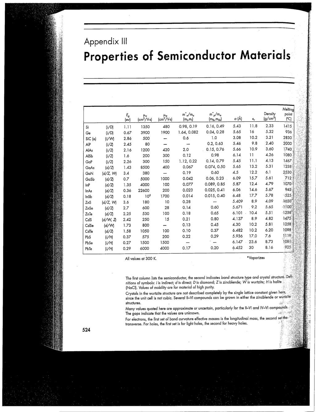
1 University of Texas Arlington Department of Electrical Engineering Nanotechnology Microelectromechanical Systems Ph.D. Diagnostic Examination Fall 2011 November 19, 2011 Question # To be filled by the student Check to have this question graded. Check only 2. To be filled by the graders Grade Grade Average TOTAL: GRADE OUT of 100: THIS EXAM PACKET HAS 9 SHEETS INCLUDING THE HELPFUL EQUATIONS AND CONSTANTS.
2 1. (50 pts) Following plot shows a typical spectral content of a lamp used for optical lithography. (a) Identify the DUV and UV regions on the plot? (10 points) (b) What wavelength of the lamp output should be most suitable for the 250 nm technology and below? (10 points) (c) Considering NA 0.5 and using phase-shifting mask, what minimum feature size can be achieved with the wavelength of question (b)? (15 points) (d) What would be expected depth of field for this system? (15 points)
3 2. (50 points) Congratulations, you have just discovered a new semiconductor, utaium which has a cubic crystal structure. The E-k relationship is shown in the figure below. The conduction bands A and B have the same energy minima E c. Conduction Band B Conduction Band A E c E v Valence Band L [111] [100] X a) Draw the constant energy surface(s) for electrons near the conduction band minima in k-space. b) Given the following inverse effective mass tensor data measured by cyclotron resonance at 4 K. Calculate the density of states effective mass for the conduction band, m n *. Conduction Band A m o m* m o =9.1 x kg Conduction Band B m o m* c) Given the effective mass data for the valence bands are m hh =0.347m o, m lh =0.0429m o, and m so =0.077m o ; determine the density of states effective mass for holes in the valence band m p *. Assume parabolic constant energy surfaces at the band minima. 2 4 ab Note: The volume of a prolate spheroid is where 2a and 2b are the 3 lengths of the major and minor axes respectively of the rotated ellipse.
4 3. (50 pts) Crystalline silicon has a lattice constant of Å and an atomic weight of gm/mole. a) What is the Bravais lattice of Si? b) What is the crystal structure of Si? c) What is the crystal system of Si? d) What are the symmetry properties of Si? e) How many atoms are there per unit cell? f) What is the mass density of Si?
5 COLOR CHART FOR THERMALLY GROWN SiO 2 FILMS (OBSERVED PERPENDICULARLY UNDER DAYLIGHT FLURORESCENT LIGHTING) OXIDE NITRIDE Film Thickness Order (Microns) (5450 A) Color and Comments A Tan Brown Dark Violet to red violet Royal blue Light blue to metallic blue Metallic to very light yellow-green Light gold or yellow slightly metallic Gold with slight yellow-orange Orange to Melon Red-Violet Blue to violet-blue Blue Blue to blue-green Light green Green to yellow-green Yellow-green Green- yellow Yellow Light orange Carnation pink Violet-red Red-violet Violet Blue Violet Blue Blue-green Green (Broad) Yellow-green Green-yellow Yellow to Yellowish (not yellow but is in the position where yellow is to be expected. At times is appears to be light creamy gray or metallic) Light orange or yellow to pink borderline Carnation pink Violet-red OXIDE NITRIDE Film Thickness Order (Microns) (5450 A) Bluish (Not blue but borderline between violet and blue-green. It appears more like a Mixture between violet -red and blue-green and over-all looks grayish Blue-green to green (quite broad Yellowish Orange (rather broad for orange) Salmon Dull, light red-violet Violet Blue-violet Blue Blue-green Dull yellow-green Yellow to Yellowish Orange Carnation Pink Violet-red Red-violet Violet Blue-violet Green Yellow-green Green Violet Red-violet Violet-red Carnation Pink-Salmon Orange Yellowish Sky blue to green-blue Orange Violet Blue-violet 1.50 Blue Dull Yellow-green
6 Physical Constants (in units frequently used in semiconductor electronics) Electronic charge q x C Speed of light in vacuum c x cm s -1 Permittivity of vacuum ε x F cm -1 Free electron mass m x kg Planck's constant h x J s x ev s Boltzmann's constant k 1.38 x J K x 10-5 ev K -1 Avogadro's number A x molecules (g mole) -1 Thermal voltage V t =kt/q at 80.6 F (300K) mv 68 F (293K) mv Conversion Factors 1 Ǻ = 10-8 cm = 0.1nm 1 mil = 10-3 inch = 25.4 µm 1 ev = x J 1 J = 10 7 erg
7
8
9
UNIVERSITY OF CALIFORNIA College of Engineering Department of Electrical Engineering and Computer Sciences. Professor Ali Javey. Spring 2009.
 UNIVERSITY OF CALIFORNIA College of Engineering Department of Electrical Engineering and Computer Sciences EE143 Professor Ali Javey Spring 2009 Exam 1 Name: SID: Closed book. One sheet of notes is allowed.
Quiz #1 Practice Problem Set
 Name: Student Number: ELEC 3908 Physical Electronics Quiz #1 Practice Problem Set? Minutes January 22, 2016 - No aids except a non-programmable calculator - All questions must be answered - All questions
UNIVERSITY OF CALIFORNIA College of Engineering Department of Electrical Engineering and Computer Sciences. Professor Ali Javey. Fall 2009.
 UNIVERSITY OF CALIFORNIA College of Engineering Department of Electrical Engineering and Computer Sciences EE143 Professor Ali Javey Fall 2009 Exam 1 Name: SID: Closed book. One sheet of notes is allowed.
Midterm I - Solutions
 UNIVERSITY OF CALIFORNIA College of Engineering Department of Electrical Engineering and Computer Sciences EECS 130 Spring 2008 Professor Chenming Hu Midterm I - Solutions Name: SID: Grad/Undergrad: Closed
UNIVERSITY OF CALIFORNIA College of Engineering Department of Electrical Engineering and Computer Sciences. Fall Exam 1
 UNIVERSITY OF CALIFORNIA College of Engineering Department of Electrical Engineering and Computer Sciences EECS 143 Fall 2008 Exam 1 Professor Ali Javey Answer Key Name: SID: 1337 Closed book. One sheet
UNIVERSITY OF CALIFORNIA, BERKELEY College of Engineering Department of Electrical Engineering and Computer Sciences
 UNIVERSITY OF CALIFORNIA, BERKELEY College of Engineering Department of Electrical Engineering and Computer Sciences EE 105: Microelectronic Devices and Circuits Spring 2008 MIDTERM EXAMINATION #1 Time
1 Name: Student number: DEPARTMENT OF PHYSICS AND PHYSICAL OCEANOGRAPHY MEMORIAL UNIVERSITY OF NEWFOUNDLAND. Fall :00-11:00
 1 Name: DEPARTMENT OF PHYSICS AND PHYSICAL OCEANOGRAPHY MEMORIAL UNIVERSITY OF NEWFOUNDLAND Final Exam Physics 3000 December 11, 2012 Fall 2012 9:00-11:00 INSTRUCTIONS: 1. Answer all seven (7) questions.
3.15 Electrical, Optical, and Magnetic Materials and Devices Caroline A. Ross Fall Term, 2005
 3.15 Electrical, Optical, and Magnetic Materials and Devices Caroline A. Ross Fall Term, 2005 Exam 2 (5 pages) Closed book exam. Formulae and data are on the last 3.5 pages of the exam. This takes 80 min
UNIVERSITY OF CALIFORNIA College of Engineering Department of Electrical Engineering and Computer Sciences. Professor Chenming Hu.
 UNIVERSITY OF CALIFORNIA College of Engineering Department of Electrical Engineering and Computer Sciences EECS 130 Spring 2009 Professor Chenming Hu Midterm I Name: Closed book. One sheet of notes is
ECEN 3320 Semiconductor Devices Final exam - Sunday December 17, 2000
 Your Name: ECEN 3320 Semiconductor Devices Final exam - Sunday December 17, 2000 1. Review questions a) Illustrate the generation of a photocurrent in a p-n diode by drawing an energy band diagram. Indicate
LN 3 IDLE MIND SOLUTIONS
 IDLE MIND SOLUTIONS 1. Let us first look in most general terms at the optical properties of solids with band gaps (E g ) of less than 4 ev, semiconductors by definition. The band gap energy (E g ) can
UNIVERSITY OF CALIFORNIA College of Engineering Department of Electrical Engineering and Computer Sciences. EECS 130 Professor Ali Javey Fall 2006
 UNIVERSITY OF CALIFORNIA College of Engineering Department of Electrical Engineering and Computer Sciences EECS 130 Professor Ali Javey Fall 2006 Midterm 2 Name: SID: Closed book. Two sheets of notes are
2.57/2.570 Midterm Exam No. 1 April 4, :00 am -12:30 pm
 Name:.57/.570 Midterm Exam No. April 4, 0 :00 am -:30 pm Instructions: ().57 students: try all problems ().570 students: Problem plus one of two long problems. You can also do both long problems, and one
UNIVERSITY OF CALIFORNIA, BERKELEY College of Engineering Department of Electrical Engineering and Computer Sciences
 UNIVERSITY OF CALIFORNIA, BERKELEY College of Engineering Department of Electrical Engineering and Computer Sciences EECS 40 Spring 2000 Introduction to Microelectronic Devices Prof. King MIDTERM EXAMINATION
EPL213 Problem sheet 1
 Fundamentals of Semiconductors EPL213 Problem sheet 1 1 Aim: understanding unit cell, crystal structures, Brillouin zone, symmetry representation 1. Sketch the unit cell in these two examples. Can you
Solution 11:00 AM, Wednesday February 10, 2010, 108 Nedderman Hall 80 minutes allowed (last four digits of your student #) ( if new)
 ( if new)") MidTerm - EE 5342 (print last name) (print first name) Solution 11:00 AM, Wednesday February 10, 2010, 108 Nedderman Hall 80 minutes allowed (last four digits of your student #) (e-mail if new) Instructions:
MidTerm - EE 5342 (print last name) (print first name) Solution 11:00 AM, Wednesday February 10, 2010, 108 Nedderman Hall 80 minutes allowed (last four digits of your student #) (e-mail if new) Instructions:
3.15 Electrical, Optical, and Magnetic Materials and Devices Caroline A. Ross Fall Term, 2006
 3.15 Electrical, Optical, and Magnetic Materials and Devices Caroline A. Ross Fall Term, 2006 Exam 2 (6 pages) Closed book exam. Formulae and data are on the last 4 pages of the exam. This takes 80 min
Module 6 : PHYSICS OF SEMICONDUCTOR DEVICES Lecture 32 : Bonding in Solids
 Module 6 : PHYSICS OF SEMICONDUCTOR DEVICES Lecture 32 : Bonding in Solids Objectives In this course you will learn the following Bonding in solids. Ionic and covalent bond. Structure of Silicon Concept
ELECTRONIC DEVICES AND CIRCUITS SUMMARY
 ELECTRONIC DEVICES AND CIRCUITS SUMMARY Classification of Materials: Insulator: An insulator is a material that offers a very low level (or negligible) of conductivity when voltage is applied. Eg: Paper,
Self-study problems and questions Processing and Device Technology, FFF110/FYSD13
 Self-study problems and questions Processing and Device Technology, FFF110/FYSD13 Version 2016_01 In addition to the problems discussed at the seminars and at the lectures, you can use this set of problems
Electron Energy, E E = 0. Free electron. 3s Band 2p Band Overlapping energy bands. 3p 3s 2p 2s. 2s Band. Electrons. 1s ATOM SOLID.
 Electron Energy, E Free electron Vacuum level 3p 3s 2p 2s 2s Band 3s Band 2p Band Overlapping energy bands Electrons E = 0 1s ATOM 1s SOLID In a metal the various energy bands overlap to give a single
UNIVERSITY OF CALIFORNIA College of Engineering Department of Electrical Engineering and Computer Sciences. EECS 130 Professor Ali Javey Fall 2006
 UNIVERSITY OF CALIFORNIA College of Engineering Department of Electrical Engineering and Computer Sciences EECS 130 Professor Ali Javey Fall 2006 Midterm I Name: Closed book. One sheet of notes is allowed.
Chemistry 1A Midterm Exam 1 February 12, Potentially Useful Information. Violet Blue Green Yellow Orange Red Wavelength (nm)
") Chemistry 1A Midterm Exam 1 February 12, 2013 Professor Pines 5 pages total Student Name: Student ID#: Potentially Useful Information Violet Blue Green Yellow Orange Red 400 500 600 700 Wavelength (nm)
Chemistry 1A Midterm Exam 1 February 12, 2013 Professor Pines 5 pages total Student Name: Student ID#: Potentially Useful Information Violet Blue Green Yellow Orange Red 400 500 600 700 Wavelength (nm)
Lecture contents. Stress and strain Deformation potential. NNSE 618 Lecture #23
 1 Lecture contents Stress and strain Deformation potential Few concepts from linear elasticity theory : Stress and Strain 6 independent components 2 Stress = force/area ( 3x3 symmetric tensor! ) ij ji
A Wave of Cooperation
 A Wave of Cooperation The students will peer teach in cooperative learning groups some basic topics regarding waves. Materials: Student sheets Note sheets Procedure: 1. Place students into home teams of
Two-dimensional lattice
 Two-dimensional lattice a 1 *, k x k x =0,k y =0 X M a 2, y Γ X a 2 *, k y a 1, x Reciprocal lattice Γ k x = 0.5 a 1 *, k y =0 k x = 0, k y = 0.5 a 2 * k x =0.5a 1 *, k y =0.5a 2 * X X M k x = 0.25 a 1
UNIVERSITY OF CALIFORNIA. College of Engineering. Department of Electrical Engineering and Computer Sciences. Professor Ali Javey.
 UNIVERSITY OF CALIFORNIA College of Engineering Department of Electrical Engineering and Computer Sciences EE 143 Professor Ali Javey Spring 2009 Exam 2 Name: SID: Closed book. One sheet of notes is allowed.
Lecture 18: Semiconductors - continued (Kittel Ch. 8)
") Lecture 18: Semiconductors - continued (Kittel Ch. 8) + a - Donors and acceptors J U,e e J q,e Transport of charge and energy h E J q,e J U,h Physics 460 F 2006 Lect 18 1 Outline More on concentrations
Lecture 18: Semiconductors - continued (Kittel Ch. 8) + a - Donors and acceptors J U,e e J q,e Transport of charge and energy h E J q,e J U,h Physics 460 F 2006 Lect 18 1 Outline More on concentrations
FYS 3028/8028 Solar Energy and Energy Storage. Calculator with empty memory Language dictionaries
 Faculty of Science and Technology Exam in: FYS 3028/8028 Solar Energy and Energy Storage Date: 11.05.2016 Time: 9-13 Place: Åsgårdvegen 9 Approved aids: Type of sheets (sqares/lines): Number of pages incl.
Chemistry 6 10:00 Section Time limit = 3 hours Spring There are two sections to this exam. Please read the instructions carefully.
 Chemistry 6 10:00 Section Final Exam Time limit = 3 hours Spring 2005 Name There are two sections to this exam. Please read the instructions carefully. In the first section, there are 13 multiple choice
Electrons are shared in covalent bonds between atoms of Si. A bound electron has the lowest energy state.
 Photovoltaics Basic Steps the generation of light-generated carriers; the collection of the light-generated carriers to generate a current; the generation of a large voltage across the solar cell; and
6.012 Electronic Devices and Circuits
 Page 1 of 10 YOUR NAME Department of Electrical Engineering and Computer Science Massachusetts Institute of Technology 6.012 Electronic Devices and Circuits Exam No. 2 Thursday, November 5, 2009 7:30 to
Chem 1A, Fall 2015, Midterm Exam 1. Version A September 21, 2015 (Prof. Head-Gordon) 2
 2") Chem 1A, Fall 2015, Midterm Exam 1. Version A September 21, 2015 (Prof. Head-Gordon) 2 Name: Student ID: TA: Contents: 9 pages A. Multiple choice (7 points) B. Stoichiometry (10 points) C. Photoelectric
Chem 1A, Fall 2015, Midterm Exam 1. Version A September 21, 2015 (Prof. Head-Gordon) 2 Name: Student ID: TA: Contents: 9 pages A. Multiple choice (7 points) B. Stoichiometry (10 points) C. Photoelectric
Practical 1P4 Energy Levels and Band Gaps
 Practical 1P4 Energy Levels and Band Gaps What you should learn from this practical Science This practical illustrates some of the points from the lecture course on Elementary Quantum Mechanics and Bonding
MCQs E M WAVES. Physics Without Fear.
 MCQs E M WAVES Physics Without Fear Electromagnetic Waves At A Glance Ampere s law B. dl = μ 0 I relates magnetic fields due to current sources. Maxwell argued that this law is incomplete as it does not
Lecture 3: Optical Properties of Insulators, Semiconductors, and Metals. 5 nm
 Metals Lecture 3: Optical Properties of Insulators, Semiconductors, and Metals 5 nm Course Info Next Week (Sept. 5 and 7) no classes First H/W is due Sept. 1 The Previous Lecture Origin frequency dependence
Two-dimensional lattice
 1 Two-dimensional lattice a 1 *, k x k x = 0, k y = 0 X M a 2, y a 1, x Γ X a 2 *, k y k x = 0.5 a 1 *, k y = 0 k x = 0, k y = 0.5 a 2 * Γ k x = 0.5 a 1 *, k y = 0.5 a 2 * X X M k x = 0.25 a 1 *, k y =
MSE410/ECE 340: Electrical Properties of Materials Fall 2016 School of Materials Science and Engineering Boise State University
 MSE410/ECE 340: Electrical Properties of Materials Fall 2016 School of Materials Science and Engineering Boise State University Practice Midterm Exam October 2016 Read the questions carefully Label all
Kavli Workshop for Journalists. June 13th, CNF Cleanroom Activities
 Kavli Workshop for Journalists June 13th, 2007 CNF Cleanroom Activities Seeing nm-sized Objects with an SEM Lab experience: Scanning Electron Microscopy Equipment: Zeiss Supra 55VP Scanning electron microscopes
LECTURE 5 SUMMARY OF KEY IDEAS
 LECTURE 5 SUMMARY OF KEY IDEAS Etching is a processing step following lithography: it transfers a circuit image from the photoresist to materials form which devices are made or to hard masking or sacrificial
Observation of Atomic Spectra
 Observation of Atomic Spectra Introduction In this experiment you will observe and measure the wavelengths of different colors of light emitted by atoms. You will first observe light emitted from excited
Lecture 3: Heterostructures, Quasielectric Fields, and Quantum Structures
 Lecture 3: Heterostructures, Quasielectric Fields, and Quantum Structures MSE 6001, Semiconductor Materials Lectures Fall 2006 3 Semiconductor Heterostructures A semiconductor crystal made out of more
ET3034TUx Utilization of band gap energy
 ET3034TUx - 3.3.1 - Utilization of band gap energy In the last two weeks we have discussed the working principle of a solar cell and the external parameters that define the performance of a solar cell.
LM-79 Report TEST REPORT NO. L523A
 LM-79 Report TEST REPORT NO. L523A Test Result Summary Luminaire Manufacturer Pioneer Engineering Inc. Luminaire Model Number S ST-0246-5L-5K-120 Input Voltage RMS (V) 120.03 Input Current RMS (A) 0.28
p = {470.5 [1+(N i 2.23E17) ]}+44.9, in cm 2 /V-sec. 14. For electrons in silicon doped primarily with phosphorous, assume
![p = {470.5 [1+(N i 2.23E17) ]}+44.9, in cm 2 /V-sec. 14. For electrons in silicon doped primarily with phosphorous, assume](/thumbs/88/117111080.jpg "p = {470.5 [1+(N i 2.23E17) ]}+44.9, in cm 2 /V-sec. 14. For electrons in silicon doped primarily with phosphorous, assume") Final - EE 5340/001 (print last name) (print first name) SOLUTION Wednesday, December 15, 2010, 11:00 AM, 108 Nedderman Hall 2 hr 30 min allowed (last four digits of your student #) (e-mail if new) Instructions:
Final - EE 5340/001 (print last name) (print first name) SOLUTION Wednesday, December 15, 2010, 11:00 AM, 108 Nedderman Hall 2 hr 30 min allowed (last four digits of your student #) (e-mail if new) Instructions:
Supporting Information. Direct n- to p-type Channel Conversion in Monolayer/Few-Layer WS 2 Field-Effect Transistors by Atomic Nitrogen Treatment
 Supporting Information Direct n- to p-type Channel Conversion in Monolayer/Few-Layer WS 2 Field-Effect Transistors by Atomic Nitrogen Treatment Baoshan Tang 1,2,, Zhi Gen Yu 3,, Li Huang 4, Jianwei Chai
Practical 1P4 Energy Levels and Band Gaps
 Practical 1P4 Energy Levels and Band Gaps What you should learn from this practical Science This practical illustrates some of the points from the lecture course on Elementary Quantum Mechanics and Bonding
n from which can be derived that
 page 1 of 10 Name Last 5 digits of Student Number: XXX X (may be the same as your social security number) Chem 103 Sample Examination #3 This exam consists of ten (10) pages, including this cover page.
ACTIVITY 2 Exploring Light Patterns
 Name: Class: SOLIDS & Visual Quantum Mechanics LIGHT ACTIVITY 2 Exploring Light Patterns Goal We will continue to investigate the properties of LEDs and the incandescent lamp by observing and exploring
OPSE FINAL EXAM Fall 2015 YOU MUST SHOW YOUR WORK. ANSWERS THAT ARE NOT JUSTIFIED WILL BE GIVEN ZERO CREDIT.
 CLOSED BOOK. Equation Sheet is provided. YOU MUST SHOW YOUR WORK. ANSWERS THAT ARE NOT JUSTIFIED WILL BE GIVEN ZERO CREDIT. ALL NUMERICAL ANSERS MUST HAVE UNITS INDICATED. (Except dimensionless units like
Chem 115 Sample Examination #3
 _ Chem 115 Sample Examination #3 Student Number: This exam consists of seven (7) pages, including this cover page. Be sure your copy is complete before beginning your work. If this test packet is defective,
Write the electron configuration for Chromium (Cr):
:") Write the electron configuration for Chromium (Cr): Energy level Aufbau Principle Atomic orbital Quantum Hund s Rule Atomic number Electron Configuration Whole number Pauli Exlcusion Principle Quantum
Write the electron configuration for Chromium (Cr): Energy level Aufbau Principle Atomic orbital Quantum Hund s Rule Atomic number Electron Configuration Whole number Pauli Exlcusion Principle Quantum
PH 102 Exam III SOLUTION
 PH 102 Exam III SOLUTION Part I: Multiple choice (50%) November 30, 2007 P. LeClair 1. Answer all multiple choice problems. 2. No partial credit will be given for multiple choice questions. 1. What energy
Sample Exam # 2 ECEN 3320 Fall 2013 Semiconductor Devices October 28, 2013 Due November 4, 2013
 Sample Exam # 2 ECEN 3320 Fall 203 Semiconductor Devices October 28, 203 Due November 4, 203. Below is the capacitance-voltage curve measured from a Schottky contact made on GaAs at T 300 K. Figure : Capacitance
Optical Properties of Solid from DFT
 Optical Properties of Solid from DFT 1 Prof.P. Ravindran, Department of Physics, Central University of Tamil Nadu, India & Center for Materials Science and Nanotechnology, University of Oslo, Norway http://folk.uio.no/ravi/cmt15
Examination Radiation Physics - 8N120, 2 November
 Examination Radiation Physics - 8N0, November 0-4.00-7.00 Four general remarks: This exam consists of 6 assignments on a total of pages. There is a table on page listing the maximum number of that can
Topics in the November 2014 Exam Paper for CHEM1101
 November 2014 Topics in the November 2014 Exam Paper for CHEM1101 Click on the links for resources on each topic. 2014-N-2: 2014-N-3: 2014-N-4: 2014-N-5: 2014-N-7: 2014-N-8: 2014-N-9: 2014-N-10: 2014-N-11:
Lecture 3b. Bonding Model and Dopants. Reading: (Cont d) Notes and Anderson 2 sections
 Notes and Anderson 2 sections") Lecture 3b Bonding Model and Dopants Reading: (Cont d) Notes and Anderson 2 sections 2.3-2.7 The need for more control over carrier concentration Without help the total number of carriers (electrons and
Lecture 3b Bonding Model and Dopants Reading: (Cont d) Notes and Anderson 2 sections 2.3-2.7 The need for more control over carrier concentration Without help the total number of carriers (electrons and
Junction Diodes. Tim Sumner, Imperial College, Rm: 1009, x /18/2006
 Junction Diodes Most elementary solid state junction electronic devices. They conduct in one direction (almost correct). Useful when one converts from AC to DC (rectifier). But today diodes have a wide
Lecture 1. Introduction to Electronic Materials. Reading: Pierret 1.1, 1.2, 1.4,
 Lecture 1 Introduction to Electronic Materials Reading: Pierret 1.1, 1.2, 1.4, 2.1-2.6 Atoms to Operational Amplifiers The goal of this course is to teach the fundamentals of non-linear circuit elements
Chapter Two. Energy Bands and Effective Mass
 Chapter Two Energy Bands and Effective Mass Energy Bands Formation At Low Temperature At Room Temperature Valence Band Insulators Metals Effective Mass Energy-Momentum Diagrams Direct and Indirect Semiconduction
Fall 2012 Qualifying Exam. Part I
 Fall 2012 Qualifying Exam Part I Calculators are allowed. No reference material may be used. Please clearly mark the problems you have solved and want to be graded. Do only mark the required number of
Variation of Energy Bands with Alloy Composition E
 Variation of Energy Bands with Alloy Composition E 3.0 E.8.6 L 0.3eV Al x GaAs AlAs 1- xas 1.43eV.16eV X k.4 L. X.0 X 1.8 L 1.6 1.4 0 0. 0.4 0.6 X 0.8 1 1 Carriers in intrinsic Semiconductors Ec 4º 1º
Lab 4: Mineral Identification April 14, 2009
 Name: Lab 4: Mineral Identification April 14, 2009 While about 3000 minerals have been recognized as valid species, very few of these are commonly seen. Comprehensive mineralogy texts typically deal with
ASSESSMENT UNIT PH5: FIELDS, FORCES AND NUCLEI. A.M. WEDNESDAY, 11 June hours
 Candidate Name Centre Number 2 Candidate Number GCE A level 545/0 PHYSICS ASSESSMENT UNIT PH5: FIELDS, FORCES AND NUCLEI A.M. WEDNESDAY, June 2008 2 hours ADDITIONAL MATERIALS In addition to this paper,
Cosmology. Distinction Course. Modules 4, 5, 6 and 7 (including Residential 2) 2005 HIGHER SCHOOL CERTIFICATE EXAMINATION. Total marks 120.
 2005 HIGHER SCHOOL CERTIFICATE EXAMINATION. Total marks 120.") 2005 HIGHER SCHOOL CERTIFICATE EXAMINATION Cosmology Distinction Course Modules 4, 5, 6 and 7 (including Residential 2) Total marks 120 Section I Page 2 General Instructions Reading time 5 minutes Working
2005 HIGHER SCHOOL CERTIFICATE EXAMINATION Cosmology Distinction Course Modules 4, 5, 6 and 7 (including Residential 2) Total marks 120 Section I Page 2 General Instructions Reading time 5 minutes Working
Laboratory Atomic Emission Spectrum
 Laboratory Atomic Emission Spectrum Pre-Lab Questions: Answer the following questions in complete sentences by reading through the Overview and Background sections below. 1. What is the purpose of the
Lecture 2. Unit Cells and Miller Indexes. Reading: (Cont d) Anderson 2 1.8,
 Anderson 2 1.8,") Lecture 2 Unit Cells and Miller Indexes Reading: (Cont d) Anderson 2 1.8, 2.1-2.7 Unit Cell Concept The crystal lattice consists of a periodic array of atoms. Unit Cell Concept A building block that can
Lecture 2 Unit Cells and Miller Indexes Reading: (Cont d) Anderson 2 1.8, 2.1-2.7 Unit Cell Concept The crystal lattice consists of a periodic array of atoms. Unit Cell Concept A building block that can
Topics in the November 2009 Exam Paper for CHEM1101
 November 2009 Topics in the November 2009 Exam Paper for CHEM1101 Click on the links for resources on each topic. 2009-N-2: 2009-N-3: 2009-N-4: 2009-N-5: 2009-N-6: 2009-N-7: 2009-N-8: 2009-N-9: 2009-N-10:
Chapter VI: Ionizations and excitations
 Chapter VI: Ionizations and excitations 1 Content Introduction Ionization in gases Ionization in solids Fano factor 2 Introduction (1) Ionizations created by charged particles (incident particles or particles
Lecture 6 Plasmas. Chapters 10 &16 Wolf and Tauber. ECE611 / CHE611 Electronic Materials Processing Fall John Labram 1/68
 Lecture 6 Plasmas Chapters 10 &16 Wolf and Tauber 1/68 Announcements Homework: Homework will be returned to you on Thursday (12 th October). Solutions will be also posted online on Thursday (12 th October)
EXPERIMENT 17: Atomic Emission
 EXPERIMENT 17: Atomic Emission PURPOSE: To construct an energy level diagram of the hydrogen atom To identify an element from its line spectrum. PRINCIPLES: White light, such as emitted by the sun or an
OLIVINES, PYROXENES, AND AMPHIBOLES PLEOCHROISM, INTERFERENCE COLORS AND EXTINCTION ANGLES
 GLY 4200C Lab Exercise 12 Pleochroism OLIVINES, PYROXENES, AND AMPHIBOLES PLEOCHROISM, INTERFERENCE COLORS AND EXTINCTION ANGLES When minerals are viewed under PP they may show color. Many minerals are
AS PHYSICS. Electricity Homework Questions. moulsham high school
 moulsham high school AS PHYSCS Electricity Homework Questions Work with other memebrs of the group to complete at least the first 5 questions using your text books and your knowledge from GCSE. 1.List
Science Lab I Properties of Light
 Art & Science of Light Fall 2007 Science Lab I Properties of Light Prepared by: Dr. Dharshi Bopegedera 1 Using the Filtergraph (15 minutes) 1. Turn on the filtergraph, place a card on it and look at the
The Emission Spectra of Light
 The Emission Spectra of Light Objectives: Theory: 1.... measured the wavelength limits of the color bands in the visible spectrum, 2.... measured the wavelengths of the emission lines of the hydrogen Balmer
Atomic Spectroscopy. Objectives
 Atomic Spectroscopy Name Objectives explain the difference between emission and absorption spectra calculate the energy of orbits in the Bohr model of hydrogen calculate E for energy transitions in the
NNIN Nanotechnology Education
 NNIN Nanotechnology Education Teacher s Preparatory Guide Modeling Self-Assembly, Part II: The Water Maze Purpose The Water Maze is a reinforcement challenge activity to The Fly Prison, and relates to
LM-79 Report TEST REPORT NO.M037D
 LM-79 Report TEST REPORT NO.M037D Test Result Summary Luminaire Manufacturer Luminaire Model Number Input Voltage RMS (V) 120.0 Input Current RMS (A) 0.231 Input Power (W) 27.47 Light Output (lm) 3524
Resistivity and Temperature Coefficients (at 20 C)
") Homework # 4 Resistivity and Temperature Coefficients (at 0 C) Substance Resistivity, Temperature ( m) Coefficient, (C ) - Conductors Silver.59 x 0-0.006 Copper.6 x 0-0.006 Aluminum.65 x 0-0.0049 Tungsten
Homework # 4 Resistivity and Temperature Coefficients (at 0 C) Substance Resistivity, Temperature ( m) Coefficient, (C ) - Conductors Silver.59 x 0-0.006 Copper.6 x 0-0.006 Aluminum.65 x 0-0.0049 Tungsten
THE UNIVERSITY OF NEW SOUTH WALES SCHOOL OF PHYSICS FINAL EXAMINATION JUNE/JULY PHYS3080 Solid State Physics
 THE UNIVERSITY OF NEW SOUTH WALES SCHOOL OF PHYSICS FINAL EXAMINATION JUNE/JULY 006 PHYS3080 Solid State Physics Time Allowed hours Total number of questions - 5 Answer ALL questions All questions are
ECE 442. Spring, Lecture -2
 ECE 442 Power Semiconductor Devices and Integrated circuits Spring, 2006 University of Illinois at Chicago Lecture -2 Semiconductor physics band structures and charge carriers 1. What are the types of
University of California, Berkeley Physics H7C Spring 2011 (Yury Kolomensky) THE FINAL EXAM Monday, May 9, 7 10pm. Maximum score: 200 points
 THE FINAL EXAM Monday, May 9, 7 10pm. Maximum score: 200 points") 1 University of California, Berkeley Physics H7C Spring 2011 (Yury Kolomensky) THE FINAL EXAM Monday, May 9, 7 10pm Maximum score: 200 points NAME: SID #: You are given 180 minutes for this exam. You are
1 University of California, Berkeley Physics H7C Spring 2011 (Yury Kolomensky) THE FINAL EXAM Monday, May 9, 7 10pm Maximum score: 200 points NAME: SID #: You are given 180 minutes for this exam. You are
(2) A two-dimensional solid has an electron energy band of the form, . [1]
![(2) A two-dimensional solid has an electron energy band of the form, . [1]](/thumbs/96/128751828.jpg "(2) A two-dimensional solid has an electron energy band of the form, . [1]") (1) The figure shows a two-dimensional periodic lattice, containing A atoms (white) and B atoms (black). The section of lattice shown makes a 3a 4a rectangle, as shown (measured from A atom to A atom).
(1) The figure shows a two-dimensional periodic lattice, containing A atoms (white) and B atoms (black). The section of lattice shown makes a 3a 4a rectangle, as shown (measured from A atom to A atom).
CHEM N-2 November Write down an equation representing the decay mechanism of 14 C.
 CHEM1101 2008-N-2 November 2008 Write down an equation representing the decay mechanism of 14 C. 14 C 14 N + 0 6 7 1 6 The half-life of 14 C is 5730 years. What is the activity of precisely 1 g of this
1. The most important aspects of the quantum theory.
 Lecture 5. Radiation and energy. Objectives: 1. The most important aspects of the quantum theory: atom, subatomic particles, atomic number, mass number, atomic mass, isotopes, simplified atomic diagrams,
Optical Spectroscopies of Thin Films and Interfaces. Dietrich R. T. Zahn Institut für Physik, Technische Universität Chemnitz, Germany
 Optical Spectroscopies of Thin Films and Interfaces Dietrich R. T. Zahn Institut für Physik, Technische Universität Chemnitz, Germany 1. Introduction 2. Vibrational Spectroscopies (Raman and Infrared)
Mark Lundstrom 2/10/2013. SOLUTIONS: ECE 606 Homework Week 5 Mark Lundstrom Purdue University (corrected 3/26/13)
") SOLUIONS: ECE 606 Homework Week 5 Mark Lundstrom Purdue University corrected 6/13) Some of the problems below are taken/adapted from Chapter 4 in Advanced Semiconductor Fundamentals, nd. Ed. By R.F. Pierret.
SOLUIONS: ECE 606 Homework Week 5 Mark Lundstrom Purdue University corrected 6/13) Some of the problems below are taken/adapted from Chapter 4 in Advanced Semiconductor Fundamentals, nd. Ed. By R.F. Pierret.
ESE 372 / Spring 2013 / Lecture 5 Metal Oxide Semiconductor Field Effect Transistor
 Metal Oxide Semiconductor Field Effect Transistor V G V G 1 Metal Oxide Semiconductor Field Effect Transistor We will need to understand how this current flows through Si What is electric current? 2 Back
PŘEVODNÍK ARIADNA-DMC
 1500 3865 99,22 Winter White 1538 893 94,34 Carnation Light 1501 3823 99,61 Yelow Ultra Pale 1539 351 97,02 Coral 1502 744 98,40 Yelow Pale 1540 356 97,72 Terra Cota Medium 1503 743 97,02 Yelow Medium
Student Lab Investigation
 Student Lab Investigation Prediction: You have seen that white light has a definite spectrum. Would you predict that different colors of light have different spectra from each other? Will they be different
MSE 310/ECE 340: Electrical Properties of Materials Fall 2014 Department of Materials Science and Engineering Boise State University
 MSE 310/ECE 340: Electrical Properties of Materials Fall 2014 Department of Materials Science and Engineering Boise State University Practice Final Exam 1 Read the questions carefully Label all figures
Supplementary Figures
 Supplementary Figures 8 6 Energy (ev 4 2 2 4 Γ M K Γ Supplementary Figure : Energy bands of antimonene along a high-symmetry path in the Brillouin zone, including spin-orbit coupling effects. Empty circles
5.111 Lecture Summary #4 Wednesday, September 10, 2014
 5.111 Lecture Summary #4 Wednesday, September 10, 2014 Reading for today: Section 1.5 and Section 1.6. (Same sections in 5 th and 4 th editions) Read for Lecture #5: Section 1.3 Atomic Spectra, Section
GRAPHENE ON THE Si-FACE OF SILICON CARBIDE USER MANUAL
 GRAPHENE ON THE Si-FACE OF SILICON CARBIDE USER MANUAL 1. INTRODUCTION Silicon Carbide (SiC) is a wide band gap semiconductor that exists in different polytypes. The substrate used for the fabrication
Oxide growth model. Known as the Deal-Grove or linear-parabolic model
 Oxide growth model Known as the Deal-Grove or linear-parabolic model Important elements of the model: Gas molecules (oxygen or water) are incident on the surface of the wafer. Molecules diffuse through
Name: unid: Foundations of Astronomy ASTR/PHYS Final Exam
 Name: unid: Physical Constants * Foundations of Astronomy ASTR/PHYS 2500 Final Exam Gravitational constant G 6.673 x 10⁻¹¹ m 3 kg - 1 s - 2 Elementary charge e 1.602 x 10⁻¹⁹ C Vacuum permittivity ε 0 8.854
Direct and Indirect Semiconductor
 Direct and Indirect Semiconductor Allowed values of energy can be plotted vs. the propagation constant, k. Since the periodicity of most lattices is different in various direction, the E-k diagram must
Textbook: Section B, Chapter 1
 Atoms and the Periodic Table Review Sheet Textbook: Section B, Chapter 1 1. What is the Atomic number of nitrogen? 2. How many protons does nitrogen have? 3. How many electrons does nitrogen have? 4. How
sin[( t 2 Home Problem Set #1 Due : September 10 (Wed), 2008
, 2008") Home Problem Set #1 Due : September 10 (Wed), 008 1. Answer the following questions related to the wave-particle duality. (a) When an electron (mass m) is moving with the velocity of υ, what is the wave
Home Problem Set #1 Due : September 10 (Wed), 008 1. Answer the following questions related to the wave-particle duality. (a) When an electron (mass m) is moving with the velocity of υ, what is the wave