Unit 7 Sequential Circuits (Flip Flop, Registers)
|
|
|
- Estella Chandler
- 5 years ago
- Views:
Transcription
1 College of Computer and Information Sciences Department of Computer Science CSC 220: Computer Organization Unit 7 Sequential Circuits (Flip Flop, Registers)
2 2
, and is labelled S and another which will")
3 SR Flip-Flop The SR flip-flop, also known as a SR Latch, can be considered as one of the most basic sequential logic circuit possible. This simple flip-flop is basically a one-bit memory bistable device It has two inputs, one which will SET the device (meaning the output = 1 ), and is labelled S and another which will RESET the device (meaning the output = 0 ), labelled R. 3
4 4
5 5
6 6
7 7
8 8
9 9
10 Give Examples 10

11 The output of the flip flop would always change on every pulse applied to this data input. To avoid this an additional input called the CLOCK or ENABLE input is used to isolate the data input from the flip flop s latching circuitry after the desired data has been stored. The effect is that D input condition is only copied to the output Q when the clock input is active. This then forms the basis of another sequential device called a D Flip Flop. 11
12 12
. In other words the circuit produces frequency division as it now divides the input frequency by a factor of two (an octave) as Q = 1 once every two clock cycles.")
13 It can be seen from the frequency waveforms above, that by feeding back the output from Q to the input terminal D, the output pulses at Q have a frequency that are exactly one half ( ƒ/2 ) that of the input clock frequency, ( ƒ IN ). In other words the circuit produces frequency division as it now divides the input frequency by a factor of two (an octave) as Q = 1 once every two clock cycles. 13

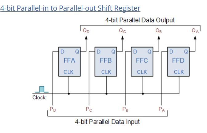
14 D Flip Flops as Data Latches A data latch can be used as a device to hold or remember the data present on its data input, thereby acting a bit like a single bit memory device and IC s such as the TTL 74LS74 or the CMOS 4042 are available in Quad format exactly for this purpose. By connecting together four, 1-bit data latches so that all their clock inputs are connected together and are clocked at the same time, a simple 4-bit Data latch can be made as shown below. 14


15 Both the S and the R inputs of the previous SR bistable have now been replaced by two inputs called the J and K inputs, respectively after its inventor Jack Kilby. Then this equates to: J = S and K = R.
16 16
17 17
18 18
19 19
20 20 Regisrers
21 21
22 22 Dr Mohamed A Berbar
23 23
24 24
25 25
26 26 Dr Mohamed A Berbar
27 MUX 2-1 MUX
28 28
29 29 Serial-in to Serial-out (SISO) Shift Register
30 30
31 Serial Parallel MUX 2-1 MUX Dr Mohamed A Berbar
32 32
33 33
34 S1 S No change Shift left (down 1 0 (Shift right (up 1 1 Parallel load 34 Dr Mohamed A Berbar
35 Other types of shift registers Logical shifts Standard shifts like we just saw. In the absence of a SI input, 0 occupies the vacant position. Left: > 1100 Right: > 0011 Circular shifts (also called ring counters or rotates) The shifted out bit wraps around to the vacant position. Left: > 0011 Right: > 1100 Switch-tail ring counter (aka Johnson counter) Similar to the ring counter, but the serial input is the complement of the serial output. Left: > 0010 Right: > 0100 Arithmetical shifts Left shifting is the same as a logical shift. Right shifting however maintains the MSB. Left: > 1100 Right: > 0011; >
36 Consider a 4-bit register with the following inputs parallel data inputs ABCD = 0011 left serial input LSI = 1 (This is the serial input for a left shift.) right serial input RSI = 0 (This is the serial input for a right shift.) The three control inputs S 2, S 1, S 0 operate as shown in the table to the right. Let the initial register content be Q A Q B Q C Q D = 0101 Example S2 S1 S0 Operation left shift circular left shift right shift circular right shift no change parallel load complement each bit set to
37 Example S2 S1 S0 Q A Q B Q C Q D S2 S1 S0 Operation left shift circular left shift right shift circular right shift no change parallel load complement each bit set to 1111 Other Information Parallel Load ABCD = 0011 LS1 1 RSI 0
38 Example S2 S1 S0 Q A Q B Q C Q D S2 S1 S0 Operation left shift circular left shift right shift circular right shift no change parallel load complement each bit set to 1111 Other Information Parallel Load ABCD = 0011 LS1 1 RSI 0
39 Example S2 S1 S0 Q A Q B Q C Q D S2 S1 S0 Operation left shift circular left shift right shift circular right shift no change parallel load complement each bit set to 1111 Other Information Parallel Load ABCD = 0011 LS1 1 RSI 0
40 Example S2 S1 S0 Q A Q B Q C Q D S2 S1 S0 Operation left shift circular left shift right shift circular right shift no change parallel load complement each bit set to 1111 Other Information Parallel Load ABCD = 0011 LS1 1 RSI 0
41 Example S2 S1 S0 Q A Q B Q C Q D S2 S1 S0 Operation left shift circular left shift right shift circular right shift no change parallel load complement each bit set to 1111 Other Information Parallel Load ABCD = 0011 LS1 1 RSI 0
42 Example S2 S1 S0 Q A Q B Q C Q D S2 S1 S0 Operation left shift circular left shift right shift circular right shift no change parallel load complement each bit set to 1111 Other Information Parallel Load ABCD = 0011 LS1 1 RSI 0
43 Example S2 S1 S0 Q A Q B Q C Q D S2 S1 S0 Operation left shift circular left shift right shift circular right shift no change parallel load complement each bit set to 1111 Other Information Parallel Load ABCD = 0011 LS1 1 RSI 0
44 Example S2 S1 S0 Q A Q B Q C Q D S2 S1 S0 Operation left shift circular left shift right shift circular right shift no change parallel load complement each bit set to 1111 Other Information Parallel Load ABCD = 0011 LS1 1 RSI 0
45 Example S2 S1 S0 Q A Q B Q C Q D S2 S1 S0 Operation left shift circular left shift right shift circular right shift no change parallel load complement each bit set to 1111 Other Information Parallel Load ABCD = 0011 LS1 1 RSI 0
46 Example S2 S1 S0 Q A Q B Q C Q D S2 S1 S0 Operation left shift circular left shift right shift circular right shift no change parallel load complement each bit set to 1111 Other Information Parallel Load ABCD = 0011 LS1 1 RSI 0
47 Example S2 S1 S0 Q A Q B Q C Q D S2 S1 S0 Operation left shift circular left shift right shift circular right shift no change parallel load complement each bit set to 1111 Other Information Parallel Load ABCD = 0011 LS1 1 RSI 0
LOGIC CIRCUITS. Basic Experiment and Design of Electronics. Ho Kyung Kim, Ph.D.
 Basic Experiment and Design of Electronics LOGIC CIRCUITS Ho Kyung Kim, Ph.D. hokyung@pusan.ac.kr School of Mechanical Engineering Pusan National University Digital IC packages TTL (transistor-transistor
Sample Test Paper - I
 Scheme G Sample Test Paper - I Course Name : Computer Engineering Group Marks : 25 Hours: 1 Hrs. Q.1) Attempt any THREE: 09 Marks a) Define i) Propagation delay ii) Fan-in iii) Fan-out b) Convert the following:
Boolean Algebra and Digital Logic 2009, University of Colombo School of Computing
 IT 204 Section 3.0 Boolean Algebra and Digital Logic Boolean Algebra 2 Logic Equations to Truth Tables X = A. B + A. B + AB A B X 0 0 0 0 3 Sum of Products The OR operation performed on the products of
Menu. Excitation Tables (Bonus Slide) EEL3701 EEL3701. Registers, RALU, Asynch, Synch
 EEL3701 EEL3701. Registers, RALU, Asynch, Synch") Menu Registers >Storage Registers >Shift Registers More LSI Components >Arithmetic-Logic Units (ALUs) > Carry-Look-Ahead Circuitry (skip this) Asynchronous versus Synchronous Look into my... 1 Excitation
Menu Registers >Storage Registers >Shift Registers More LSI Components >Arithmetic-Logic Units (ALUs) > Carry-Look-Ahead Circuitry (skip this) Asynchronous versus Synchronous Look into my... 1 Excitation
Sequential Logic Circuits
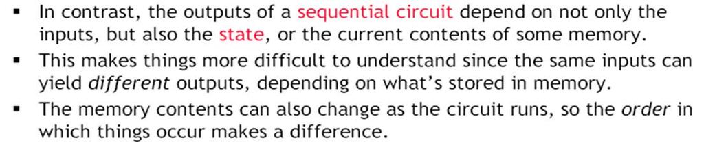
 Chapter 4 Sequential Logic Circuits 4 1 The defining characteristic of a combinational circuit is that its output depends only on the current inputs applied to the circuit. The output of a sequential circuit,
ELCT201: DIGITAL LOGIC DESIGN
 ELCT201: DIGITAL LOGIC DESIGN Dr. Eng. Haitham Omran, haitham.omran@guc.edu.eg Dr. Eng. Wassim Alexan, wassim.joseph@guc.edu.eg Lecture 6 Following the slides of Dr. Ahmed H. Madian محرم 1439 ه Winter
PGT104 Digital Electronics. PGT104 Digital Electronics
 1 Part 6 Sequential Logic ircuits Disclaimer: Most of the contents (if not all) are extracted from resources available for Digital Fundamentals 10 th Edition 2 Basic Shift Register Operations A shift register
Sequential Logic. Rab Nawaz Khan Jadoon DCS. Lecturer COMSATS Lahore Pakistan. Department of Computer Science
 Sequential Logic Rab Nawaz Khan Jadoon DCS COMSATS Institute of Information Technology Lecturer COMSATS Lahore Pakistan Digital Logic and Computer Design Sequential Logic Combinational circuits with memory
LOGIC CIRCUITS. Basic Experiment and Design of Electronics
 Basic Experiment and Design of Electronics LOGIC CIRCUITS Ho Kyung Kim, Ph.D. hokyung@pusan.ac.kr School of Mechanical Engineering Pusan National University Outline Combinational logic circuits Output
Lecture 17: Designing Sequential Systems Using Flip Flops
 EE210: Switching Systems Lecture 17: Designing Sequential Systems Using Flip Flops Prof. YingLi Tian April 11, 2019 Department of Electrical Engineering The City College of New York The City University
Shift Register Counters
 Shift Register Counters Shift register counter: a shift register with the serial output connected back to the serial input. They are classified as counters because they give a specified sequence of states.
Chapter 4. Sequential Logic Circuits
 Chapter 4 Sequential Logic Circuits 1 2 Chapter 4 4 1 The defining characteristic of a combinational circuit is that its output depends only on the current inputs applied to the circuit. The output of
CSE370 HW6 Solutions (Winter 2010)
") SE370 HW6 Solutions (Winter 2010) 1. L2e, 6.10 For this problem we are given a blank waveform with clock and input and asked to draw out the how different flip-flops and latches would behave. LK a) b)
SE370 HW6 Solutions (Winter 2010) 1. L2e, 6.10 For this problem we are given a blank waveform with clock and input and asked to draw out the how different flip-flops and latches would behave. LK a) b)
Introduction EE 224: INTRODUCTION TO DIGITAL CIRCUITS & COMPUTER DESIGN. Lecture 6: Sequential Logic 3 Registers & Counters 5/9/2010
 EE 224: INTROUCTION TO IGITAL CIRCUITS & COMPUTER ESIGN Lecture 6: Sequential Logic 3 Registers & Counters 05/10/2010 Avinash Kodi, kodi@ohio.edu Introduction 2 A Flip-Flop stores one bit of information
Design of Sequential Circuits
 Design of Sequential Circuits Seven Steps: Construct a state diagram (showing contents of flip flop and inputs with next state) Assign letter variables to each flip flop and each input and output variable
Chapter 7. Sequential Circuits Registers, Counters, RAM
 Chapter 7. Sequential Circuits Registers, Counters, RAM Register - a group of binary storage elements suitable for holding binary info A group of FFs constitutes a register Commonly used as temporary storage
Latches. October 13, 2003 Latches 1
 Latches The second part of CS231 focuses on sequential circuits, where we add memory to the hardware that we ve already seen. Our schedule will be very similar to before: We first show how primitive memory
King Fahd University of Petroleum and Minerals College of Computer Science and Engineering Computer Engineering Department
 King Fahd University of Petroleum and Minerals College of Computer Science and Engineering Computer Engineering Department Page of COE 22: Digital Logic Design (3--3) Term (Fall 22) Final Exam Sunday January
Philadelphia University Student Name: Student Number:
 Philadelphia University Student Name: Student Number: Faculty of Engineering Serial Number: Final Exam, First Semester: 2017/2018 Dept. of Computer Engineering Course Title: Logic Circuits Date: 29/01/2018
 Distributed by: www.jameco.com 1-800-831-4242 The content and copyrights of the attached material are the property of its owner. INTEGRATED CIRCUITS DATA SHEET For a complete data sheet, please also download:
Chapter 14 Sequential logic, Latches and Flip-Flops
 Chapter 14 Sequential logic, Latches and Flip-Flops Flops Lesson 4 JK Flip Flop Ch14L4-"Digital Principles and Design", Raj Kamal, Pearson Education, 2006 2 JK Flip-Flop ve edge triggered Output Q and
Digital Electronics Circuits 2017
 JSS SCIENCE AND TECHNOLOGY UNIVERSITY Digital Electronics Circuits (EC37L) Lab in-charge: Dr. Shankraiah Course outcomes: After the completion of laboratory the student will be able to, 1. Simplify, design
CHW 261: Logic Design
 CHW 26: Logic Design Instructors: Prof. Hala Zayed Dr. Ahmed Shalaby http://www.bu.edu.eg/staff/halazayed4 http://bu.edu.eg/staff/ahmedshalaby4# Slide Digital Fundamentals CHAPTER 8 Counters Slide 2 Counting
Sequential Circuit Analysis
 Sequential Circuit Analysis Last time we started talking about latches and flip-flops, which are basic one-bit memory units. Today we ll talk about sequential circuit analysis and design. First, we ll
MAHALAKSHMI ENGINEERING COLLEGE TIRUCHIRAPALLI
 DEPARTMENT: ECE MAHALAKSHMI ENGINEERING COLLEGE TIRUCHIRAPALLI 6 QUESTION BANK SUBJECT NAME: DIGITAL ELECTRONICS UNIT : Design of Sequential Circuits PART A ( Marks). Draw the logic diagram 4: Multiplexer.(AUC
EECS150 - Digital Design Lecture 11 - Shifters & Counters. Register Summary
 EECS50 - Digital Design Lecture - Shifters & Counters February 24, 2003 John Wawrzynek Spring 2005 EECS50 - Lec-counters Page Register Summary All registers (this semester) based on Flip-flops: q 3 q 2
DE58/DC58 LOGIC DESIGN DEC 2014
 Q.2 a. In a base-5 number system, 3 digit representations is used. Find out (i) Number of distinct quantities that can be represented.(ii) Representation of highest decimal number in base-5. Since, r=5
ECE/Comp Sci 352 Digital Systems Fundamentals. Charles R. Kime Section 2 Fall Logic and Computer Design Fundamentals
 University of Wisconsin - Madison ECE/Comp Sci 352 Digital Systems Fundamentals Charles R. Kime Section 2 Fall 2001 Lecture 5 Registers & Counters Part 2 Charles Kime Counters Counters are sequential circuits
EE 209 Logic Cumulative Exam Name:
 EE 209 Logic Cumulative Exam Name: 1.) Answer the following questions as True or False a.) A 4-to-1 multiplexer requires at least 4 select lines: true / false b.) An 8-to-1 mux and no other logi can be
EECS150 - Digital Design Lecture 18 - Counters
 EECS150 - Digital Design Lecture 18 - Counters October 24, 2002 John Wawrzynek Fall 2002 EECS150 - Lec18-counters Page 1 Counters Special sequential circuits (FSMs) that sequence though a set outputs.
EECS150 - Digital Design Lecture 18 - Counters
 EECS50 - Digital Design Lecture 8 - Counters October 24, 2002 John Wawrzynek Fall 2002 EECS50 - Lec8-counters Page Counters Special sequential circuits (FSMs) that sequence though a set outputs. Examples:
UNIVERSITY OF BOLTON SCHOOL OF ENGINEERING BENG (HONS) ELECTRICAL & ELECTRONICS ENGINEERING EXAMINATION SEMESTER /2017
 ELECTRICAL & ELECTRONICS ENGINEERING EXAMINATION SEMESTER /2017") UNIVERSITY OF BOLTON TW35 SCHOOL OF ENGINEERING BENG (HONS) ELECTRICAL & ELECTRONICS ENGINEERING EXAMINATION SEMESTER 2-2016/2017 INTERMEDIATE DIGITAL ELECTRONICS AND COMMUNICATIONS MODULE NO: EEE5002
UNIVERSITY OF BOLTON TW35 SCHOOL OF ENGINEERING BENG (HONS) ELECTRICAL & ELECTRONICS ENGINEERING EXAMINATION SEMESTER 2-2016/2017 INTERMEDIATE DIGITAL ELECTRONICS AND COMMUNICATIONS MODULE NO: EEE5002
SIR C.R.REDDY COLLEGE OF ENGINEERING ELURU DIGITAL INTEGRATED CIRCUITS (DIC) LABORATORY MANUAL III / IV B.E. (ECE) : I - SEMESTER
 LABORATORY MANUAL III / IV B.E. (ECE) : I - SEMESTER") SIR C.R.REDDY COLLEGE OF ENGINEERING ELURU 534 007 DIGITAL INTEGRATED CIRCUITS (DIC) LABORATORY MANUAL III / IV B.E. (ECE) : I - SEMESTER DEPARTMENT OF ELECTRONICS AND COMMUNICATION ENGINEERING DIGITAL
SIR C.R.REDDY COLLEGE OF ENGINEERING ELURU 534 007 DIGITAL INTEGRATED CIRCUITS (DIC) LABORATORY MANUAL III / IV B.E. (ECE) : I - SEMESTER DEPARTMENT OF ELECTRONICS AND COMMUNICATION ENGINEERING DIGITAL
Combinatorial Logic Design Multiplexers and ALUs CS 64: Computer Organization and Design Logic Lecture #13
 Combinatorial Logic Design Multiplexers and ALUs CS 64: Computer Organization and Design Logic Lecture #13 Ziad Matni Dept. of Computer Science, UCSB Administrative Re: Midterm Exam #2 Graded! 5/22/18
Vidyalankar S.E. Sem. III [INFT] Analog and Digital Circuits Prelim Question Paper Solution
![Vidyalankar S.E. Sem. III [INFT] Analog and Digital Circuits Prelim Question Paper Solution](/thumbs/77/75121612.jpg "Vidyalankar S.E. Sem. III [INFT] Analog and Digital Circuits Prelim Question Paper Solution") . (a). (b) S.E. Sem. III [INFT] Analog and Digital Circuits Prelim Question Paper Solution Practical Features of OpAmp (A 74) i) Large voltage gain (of the order of 2 0 5 ) ii) Very high input resistance
. (a). (b) S.E. Sem. III [INFT] Analog and Digital Circuits Prelim Question Paper Solution Practical Features of OpAmp (A 74) i) Large voltage gain (of the order of 2 0 5 ) ii) Very high input resistance
King Fahd University of Petroleum and Minerals College of Computer Science and Engineering Computer Engineering Department
 King Fahd University of Petroleum and Minerals College of Computer Science and Engineering Computer Engineering Department Page 1 of 13 COE 202: Digital Logic Design (3-0-3) Term 112 (Spring 2012) Final
EECS150 - Digital Design Lecture 17 - Sequential Circuits 3 (Counters)
") EECS150 - Digital Design Lecture 17 - Sequential Circuits 3 (Counters) March 19&21, 2002 John Wawrzynek Spring 2002 EECS150 - Lec13-seq3 version 2 Page 1 Counters Special sequential circuits (FSMs) that
EECS150 - Digital Design Lecture 17 - Sequential Circuits 3 (Counters) March 19&21, 2002 John Wawrzynek Spring 2002 EECS150 - Lec13-seq3 version 2 Page 1 Counters Special sequential circuits (FSMs) that
MAHARASHTRA STATE BOARD OF TECHNICAL EDUCATION (Autonomous) (ISO/IEC Certified) State any two Boolean laws. (Any 2 laws 1 mark each)
 (ISO/IEC Certified) State any two Boolean laws. (Any 2 laws 1 mark each)") Subject Code: 17333 Model Answer Page 1/ 27 Important Instructions to examiners: 1) The answers should be examined by key words and not as word-to-word as given in the model answer scheme. 2) The model
Subject Code: 17333 Model Answer Page 1/ 27 Important Instructions to examiners: 1) The answers should be examined by key words and not as word-to-word as given in the model answer scheme. 2) The model
Topic 8: Sequential Circuits
 Topic 8: Sequential Circuits Readings : Patterson & Hennesy, Appendix B.4 - B.6 Goals Basic Principles behind Memory Elements Clocks Applications of sequential circuits Introduction to the concept of the
Vidyalankar S.E. Sem. III [CMPN] Digital Logic Design and Analysis Prelim Question Paper Solution
![Vidyalankar S.E. Sem. III [CMPN] Digital Logic Design and Analysis Prelim Question Paper Solution](/thumbs/90/103673562.jpg "Vidyalankar S.E. Sem. III [CMPN] Digital Logic Design and Analysis Prelim Question Paper Solution") . (a) (i) ( B C 5) H (A 2 B D) H S.E. Sem. III [CMPN] Digital Logic Design and Analysis Prelim Question Paper Solution ( B C 5) H (A 2 B D) H = (FFFF 698) H (ii) (2.3) 4 + (22.3) 4 2 2. 3 2. 3 2 3. 2 (2.3)
. (a) (i) ( B C 5) H (A 2 B D) H S.E. Sem. III [CMPN] Digital Logic Design and Analysis Prelim Question Paper Solution ( B C 5) H (A 2 B D) H = (FFFF 698) H (ii) (2.3) 4 + (22.3) 4 2 2. 3 2. 3 2 3. 2 (2.3)
Digital Circuits and Systems
 EE201: Digital Circuits and Systems 4 Sequential Circuits page 1 of 11 EE201: Digital Circuits and Systems Section 4 Sequential Circuits 4.1 Overview of Sequential Circuits: Definition The circuit whose
Fundamentals of Digital Design
 Fundamentals of Digital Design Digital Radiation Measurement and Spectroscopy NE/RHP 537 1 Binary Number System The binary numeral system, or base-2 number system, is a numeral system that represents numeric
Integrated Circuits & Systems
 Federal University of Santa Catarina Center for Technology Computer Science & Electronics Engineering Integrated Circuits & Systems INE 5442 Lecture 18 CMOS Sequential Circuits - 1 guntzel@inf.ufsc.br
MODEL ANSWER SUMMER 17 EXAMINATION Subject Title: Principles of Digital Techniques
 MODEL ANSWER SUMMER 17 EXAMINATION Subject Title: Principles of Digital Techniques Subject Code: Important Instructions to examiners: 1) The answers should be examined by key words and not as word-to-word
PAST EXAM PAPER & MEMO N3 ABOUT THE QUESTION PAPERS:
 EKURHULENI TECH COLLEGE. No. 3 Mogale Square, Krugersdorp. Website: www. ekurhulenitech.co.za Email: info@ekurhulenitech.co.za TEL: 011 040 7343 CELL: 073 770 3028/060 715 4529 PAST EXAM PAPER & MEMO N3
COEN 312 DIGITAL SYSTEMS DESIGN - LECTURE NOTES Concordia University
 1 OEN 312 DIGIAL SYSEMS DESIGN - LEURE NOES oncordia University hapter 6: Registers and ounters NOE: For more examples and detailed description of the material in the lecture notes, please refer to the
ESE 570: Digital Integrated Circuits and VLSI Fundamentals
 ESE 570: Digital Integrated Circuits and VLSI Fundamentals Lec 17: March 23, 2017 Energy and Power Optimization, Design Space Exploration, Synchronous MOS Logic Lecture Outline! Energy and Power Optimization
Logic Design II (17.342) Spring Lecture Outline
 Spring Lecture Outline") Logic Design II (17.342) Spring 2012 Lecture Outline Class # 10 April 12, 2012 Dohn Bowden 1 Today s Lecture First half of the class Circuits for Arithmetic Operations Chapter 18 Should finish at least
Logic Design II (17.342) Spring 2012 Lecture Outline Class # 10 April 12, 2012 Dohn Bowden 1 Today s Lecture First half of the class Circuits for Arithmetic Operations Chapter 18 Should finish at least
DIGITAL LOGIC CIRCUITS
 DIGITAL LOGIC CIRCUITS Introduction Logic Gates Boolean Algebra Map Specification Combinational Circuits Flip-Flops Sequential Circuits Memory Components Integrated Circuits Digital Computers 2 LOGIC GATES
Dept. of ECE, CIT, Gubbi Page 1
 Verification: 1) A.B = A + B 7404 7404 7404 A B A.B A.B 0 0 0 1 0 1 0 1 1 0 0 1 1 1 1 0 A B A B A + B 0 0 1 1 1 0 1 1 0 1 1 0 0 1 1 1 1 0 0 0 2) A+B = A. B 7404 7404 7404 A B A+B A+B 0 0 0 1 0 1 1 0 1
EET 310 Flip-Flops 11/17/2011 1
 EET 310 Flip-Flops 11/17/2011 1 FF s and some Definitions Clock Input: FF s are controlled by a trigger or Clock signal. All FF s have a clock input. If a device which attempts to do a FF s task does not
MAHALAKSHMI ENGINEERING COLLEGE TIRUCHIRAPALLI
 MAHALAKSHMI ENGINEERING COLLEGE TIRUCHIRAPALLI 6 DEPARTMENT: EEE QUESTION BANK SUBJECT NAME: DIGITAL LOGIC CIRCUITS SUBJECT CODE: EE55 SEMESTER IV UNIT : Design of Synchronous Sequential Circuits PART
INTEGRATED CIRCUITS. For a complete data sheet, please also download:
 INTEGRATED CIRCUITS DATA SHEET For a complete data sheet, please also download: The IC06 74HC/HCT/HCU/HCMOS Logic Family Specifications The IC06 74HC/HCT/HCU/HCMOS Logic Package Information The IC06 74HC/HCT/HCU/HCMOS
State and Finite State Machines
 State and Finite State Machines See P&H Appendix C.7. C.8, C.10, C.11 Hakim Weatherspoon CS 3410, Spring 2013 Computer Science Cornell University Big Picture: Building a Processor memory inst register
Decoding A Counter. svbitec.wordpress.com 1
 ecoding A ounter ecoding a counter involves determining which state in the sequence the counter is in. ifferentiate between active-high and active-low decoding. Active-HIGH decoding: output HIGH if the
INTEGRATED CIRCUITS. For a complete data sheet, please also download:
 INTEGRATED CIRCUITS DATA SHEET For a complete data sheet, please also download: The IC06 74HC/HCT/HCU/HCMOS Logic Family Specifications The IC06 74HC/HCT/HCU/HCMOS Logic Package Information The IC06 74HC/HCT/HCU/HCMOS
UNIT 8A Computer Circuitry: Layers of Abstraction. Boolean Logic & Truth Tables
 UNIT 8 Computer Circuitry: Layers of bstraction 1 oolean Logic & Truth Tables Computer circuitry works based on oolean logic: operations on true (1) and false (0) values. ( ND ) (Ruby: && ) 0 0 0 0 0 1
CPE100: Digital Logic Design I
 Professor Brendan Morris, SEB 3216, brendan.morris@unlv.edu CPE100: Digital Logic Design I Midterm02 Review http://www.ee.unlv.edu/~b1morris/cpe100/ 2 Logistics Thursday Nov. 16 th In normal lecture (13:00-14:15)
MAHARASHTRA STATE BOARD OF TECHNICAL EDUCATION (Autonomous) (ISO/IEC Certified)
 (ISO/IEC Certified)") WINTER 17 EXAMINATION Subject Name: Digital Techniques Model Answer Subject Code: 17333 Important Instructions to examiners: 1) The answers should be examined by key words and not as word-to-word as given
WINTER 17 EXAMINATION Subject Name: Digital Techniques Model Answer Subject Code: 17333 Important Instructions to examiners: 1) The answers should be examined by key words and not as word-to-word as given
on candidate s understanding. 7) For programming language papers, credit may be given to any other program based on equivalent concept.
 For programming language papers, credit may be given to any other program based on equivalent concept.") WINTER 17 EXAMINATION Subject Name: Digital Techniques Model Answer Subject Code: 17333 Important Instructions to examiners: 1) The answers should be examined by key words and not as word-to-word as given
WINTER 17 EXAMINATION Subject Name: Digital Techniques Model Answer Subject Code: 17333 Important Instructions to examiners: 1) The answers should be examined by key words and not as word-to-word as given
Introduction to Digital Logic
 Introduction to Digital Logic Lecture 17: Latches Flip-Flops Problem w/ Bistables Output should have been at end of sequence Problem: Glitch was remembered Need some way to ignore inputs until they are
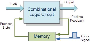
Sequential Circuits Sequential circuits combinational circuits state gate delay
 Sequential Circuits Sequential circuits are those with memory, also called feedback. In this, they differ from combinational circuits, which have no memory. The stable output of a combinational circuit
I. Motivation & Examples
 I. Motivation & Examples Output depends on current input and past history of inputs. State embodies all the information about the past needed to predict current output based on current input. State variables,
Lecture 13: Sequential Circuits, FSM
 Lecture 13: Sequential Circuits, FSM Today s topics: Sequential circuits Finite state machines Reminder: midterm on Tue 2/28 will cover Chapters 1-3, App A, B if you understand all slides, assignments,
Chapter 3 Digital Logic Structures
 Chapter 3 Digital Logic Structures Original slides from Gregory Byrd, North Carolina State University Modified by C. Wilcox, M. Strout, Y. Malaiya Colorado State University Computing Layers Problems Algorithms
Lecture 14: State Tables, Diagrams, Latches, and Flip Flop
 EE210: Switching Systems Lecture 14: State Tables, Diagrams, Latches, and Flip Flop Prof. YingLi Tian Nov. 6, 2017 Department of Electrical Engineering The City College of New York The City University
(Boolean Algebra, combinational circuits) (Binary Codes and -arithmetics)
 (Binary Codes and -arithmetics)") Task 1. Exercises: Logical Design of Digital Systems Seite: 1 Self Study (Boolean Algebra, combinational circuits) 1.1 Minimize the function f 1 a ab ab by the help of Boolean algebra and give an implementation
Task 1. Exercises: Logical Design of Digital Systems Seite: 1 Self Study (Boolean Algebra, combinational circuits) 1.1 Minimize the function f 1 a ab ab by the help of Boolean algebra and give an implementation
Chapter 7 Sequential Logic
 Chapter 7 Sequential Logic SKEE2263 Digital Systems Mun im/ismahani/izam {munim@utm.my,e-izam@utm.my,ismahani@fke.utm.my} March 28, 2016 Table of Contents 1 Intro 2 Bistable Circuits 3 FF Characteristics
3. Complete the following table of equivalent values. Use binary numbers with a sign bit and 7 bits for the value
 EGC22 Digital Logic Fundamental Additional Practice Problems. Complete the following table of equivalent values. Binary. Octal 35.77 33.23.875 29.99 27 9 64 Hexadecimal B.3 D.FD B.4C 2. Calculate the following
Arithme(c logic units and memory
 Arithme(c logic units and memory CSCI 255: Introduc/on to Embedded Systems Keith Vertanen Copyright 2011 Layers of abstrac-on abstrac(on building blocks examples computer components Macbook Pro components
S.Y. Diploma : Sem. III [CO/CM/IF/CD/CW] Digital Techniques
![S.Y. Diploma : Sem. III [CO/CM/IF/CD/CW] Digital Techniques](/thumbs/90/103932933.jpg "S.Y. Diploma : Sem. III [CO/CM/IF/CD/CW] Digital Techniques") S.Y. Diploma : Sem. III [CO/CM/IF/CD/CW] Digital Techniques Time: 3 Hrs.] Prelim Question Paper Solution [Marks : 100 Q.1(a) Attempt any SIX of the following : [12] Q.1(a) (i) Derive AND gate and OR gate
S.Y. Diploma : Sem. III [CO/CM/IF/CD/CW] Digital Techniques Time: 3 Hrs.] Prelim Question Paper Solution [Marks : 100 Q.1(a) Attempt any SIX of the following : [12] Q.1(a) (i) Derive AND gate and OR gate
Sequential vs. Combinational
 Sequential Circuits Sequential vs. Combinational Combinational Logic: Output depends only on current input TV channel selector (-9) inputs system outputs Sequential Logic: Output depends not only on current
L4: Sequential Building Blocks (Flip-flops, Latches and Registers)
") L4: Sequential Building Blocks (Flip-flops, Latches and Registers) Acknowledgements:., Materials in this lecture are courtesy of the following people and used with permission. - Randy H. Katz (University
L4: Sequential Building Blocks (Flip-flops, Latches and Registers) Acknowledgements:., Materials in this lecture are courtesy of the following people and used with permission. - Randy H. Katz (University
Lecture 10: Synchronous Sequential Circuits Design
 Lecture 0: Synchronous Sequential Circuits Design. General Form Input Combinational Flip-flops Combinational Output Circuit Circuit Clock.. Moore type has outputs dependent only on the state, e.g. ripple
CMPE12 - Notes chapter 2. Digital Logic. (Textbook Chapters and 2.1)"
") CMPE12 - Notes chapter 2 Digital Logic (Textbook Chapters 3.1-3.5 and 2.1)" Truth table" The most basic representation of a logic function." Brute force representation listing the output for all possible
CMPE12 - Notes chapter 2 Digital Logic (Textbook Chapters 3.1-3.5 and 2.1)" Truth table" The most basic representation of a logic function." Brute force representation listing the output for all possible
INTEGRATED CIRCUITS. For a complete data sheet, please also download:
 INTEGRATED CIRCUITS DATA SEET For a complete data sheet, please also download: The IC6 74C/CT/CU/CMOS Logic Family Specifications The IC6 74C/CT/CU/CMOS Logic Package Information The IC6 74C/CT/CU/CMOS
L4: Sequential Building Blocks (Flip-flops, Latches and Registers)
") L4: Sequential Building Blocks (Flip-flops, Latches and Registers) Acknowledgements: Lecture material adapted from R. Katz, G. Borriello, Contemporary Logic esign (second edition), Prentice-Hall/Pearson
L4: Sequential Building Blocks (Flip-flops, Latches and Registers) Acknowledgements: Lecture material adapted from R. Katz, G. Borriello, Contemporary Logic esign (second edition), Prentice-Hall/Pearson
CS/COE1541: Introduction to Computer Architecture. Logic Design Review. Sangyeun Cho. Computer Science Department University of Pittsburgh
 CS/COE54: Introduction to Computer Architecture Logic Design Review Sangyeun Cho Computer Science Department Logic design? Digital hardware is implemented by way of logic design Digital circuits process
Digital Fundamentals
 Digital Fundamentals Tenth Edition Floyd hapter 8 Modified by Yuttapong Jiraraksopakun Floyd, Digital Fundamentals, 10 th 2008 Pearson Education ENE, KMUTT ed 2009 ounting in Binary As you know, the binary
Lecture Outline. ESE 570: Digital Integrated Circuits and VLSI Fundamentals. Total Power. Energy and Power Optimization. Worksheet Problem 1
 ESE 570: Digital Integrated Circuits and VLSI Fundamentals Lec 16: March 20, 2018 Energy and Power Optimization, Design Space Exploration Lecture Outline! Energy and Power Optimization " Tradeoffs! Design
Digital Fundamentals
 Digital Fundamentals Tenth Edition Floyd Chapter 9 Sections 9-1 thru 9-5 2009 Pearson Education, Upper 2008 Pearson Saddle River, Education NJ 07458. All Rights Reserved ET285 Agenda Week 2 Quiz 0: Covered
GMU, ECE 680 Physical VLSI Design
 ECE680: Physical VLSI esign Chapter IV esigning Sequential Logic Circuits (Chapter 7) 1 Sequential Logic Inputs Current State COMBINATIONAL LOGIC Registers Outputs Next state 2 storage mechanisms positive
Unit II Chapter 4:- Digital Logic Contents 4.1 Introduction... 4
 Unit II Chapter 4:- Digital Logic Contents 4.1 Introduction... 4 4.1.1 Signal... 4 4.1.2 Comparison of Analog and Digital Signal... 7 4.2 Number Systems... 7 4.2.1 Decimal Number System... 7 4.2.2 Binary
Digital Logic: Boolean Algebra and Gates. Textbook Chapter 3
 Digital Logic: Boolean Algebra and Gates Textbook Chapter 3 Basic Logic Gates XOR CMPE12 Summer 2009 02-2 Truth Table The most basic representation of a logic function Lists the output for all possible
9/18/2008 GMU, ECE 680 Physical VLSI Design
 ECE680: Physical VLSI esign Chapter IV esigning Sequential Logic Circuits (Chapter 7) 1 Sequential Logic Inputs Current State COMBINATIONAL LOGIC Registers Outputs Next state 2 storage mechanisms positive
I. Motivation & Examples
 I. Motivation & Examples Output depends on current input and past history of inputs. State embodies all the information about the past needed to predict current output based on current input. State variables,
Logic design? Transistor as a switch. Layered design approach. CS/COE1541: Introduction to Computer Architecture. Logic Design Review.
 Logic design? CS/COE54: Introduction to Computer rchitecture Digital hardware is implemented by way of logic design Digital circuits process and produce two discrete values: and Example: -bit full adder
University of Toronto Faculty of Applied Science and Engineering Edward S. Rogers Sr. Department of Electrical and Computer Engineering
 University of Toronto Faculty of Applied Science and Engineering Edward S. Rogers Sr. Department of Electrical and Computer Engineering Final Examination ECE 241F - Digital Systems Examiners: J. Rose and
Digital Integrated Circuits A Design Perspective
 igital Integrated Circuits A esign Perspective Jan M. Rabaey Anantha Chandrakasan Borivoje Nikolic esigning Sequential Logic Circuits November 2002 Sequential Logic Inputs Current State COMBINATIONAL LOGIC
Computers also need devices capable of Storing data and information Performing mathematical operations on such data
 Sequential Machines Introduction Logic devices examined so far Combinational Output function of input only Output valid as long as input true Change input change output Computers also need devices capable
S.Y. Diploma : Sem. III [DE/ED/EI/EJ/EN/ET/EV/EX/IC/IE/IS/IU/MU] Principles of Digital Techniques
![S.Y. Diploma : Sem. III [DE/ED/EI/EJ/EN/ET/EV/EX/IC/IE/IS/IU/MU] Principles of Digital Techniques](/thumbs/82/86792063.jpg "S.Y. Diploma : Sem. III [DE/ED/EI/EJ/EN/ET/EV/EX/IC/IE/IS/IU/MU] Principles of Digital Techniques") S.Y. Diploma : Sem. III [DE/ED/EI/EJ/EN/ET/EV/EX/IC/IE/IS/IU/MU] Principles of Digital Techniques Time: 3 Hrs.] Prelim Question Paper Solution [Marks : 100 Q.1(a) Attempt any SIX of the following : [12]
S.Y. Diploma : Sem. III [DE/ED/EI/EJ/EN/ET/EV/EX/IC/IE/IS/IU/MU] Principles of Digital Techniques Time: 3 Hrs.] Prelim Question Paper Solution [Marks : 100 Q.1(a) Attempt any SIX of the following : [12]
Design at the Register Transfer Level
 Week-7 Design at the Register Transfer Level Algorithmic State Machines Algorithmic State Machine (ASM) q Our design methodologies do not scale well to real-world problems. q 232 - Logic Design / Algorithmic
ELEN Electronique numérique
 ELEN0040 - Electronique numérique Patricia ROUSSEAUX Année académique 2014-2015 CHAPITRE 3 Combinational Logic Circuits ELEN0040 3-4 1 Combinational Functional Blocks 1.1 Rudimentary Functions 1.2 Functions
Jan M. Rabaey Anantha Chandrakasan Borivoje Nikolic. November Digital Integrated Circuits 2nd Sequential Circuits
 igital Integrated Circuits A esign Perspective Jan M. Rabaey Anantha Chandrakasan Borivoje Nikolic esigning i Sequential Logic Circuits November 2002 Sequential Logic Inputs Current State COMBINATIONAL
EECS150 - Digital Design Lecture 25 Shifters and Counters. Recap
 EECS150 - Digital Design Lecture 25 Shifters and Counters Nov. 21, 2013 Prof. Ronald Fearing Electrical Engineering and Computer Sciences University of California, Berkeley (slides courtesy of Prof. John
Clocked Sequential Circuits UNIT 13 ANALYSIS OF CLOCKED SEQUENTIAL CIRCUITS. Analysis of Clocked Sequential Circuits. Signal Tracing and Timing Charts
 ed Sequential Circuits 2 Contents nalysis by signal tracing & timing charts State tables and graphs General models for sequential circuits sequential parity checker Reading Unit 3 asic unit Unit : Latch
Lecture 13: Sequential Circuits, FSM
 Lecture 13: Sequential Circuits, FSM Today s topics: Sequential circuits Finite state machines 1 Clocks A microprocessor is composed of many different circuits that are operating simultaneously if each
Roger L. Tokheim. Chapter 8 Counters Glencoe/McGraw-Hill
 Digital Electronics Principles & Applications Sixth Edition Roger L. Tokheim Chapter 8 Counters 2003 Glencoe/McGraw-Hill INTRODUCTION Overview of Counters Characteristics of Counters Ripple Up Counter
EE40 Lec 15. Logic Synthesis and Sequential Logic Circuits
 EE40 Lec 15 Logic Synthesis and Sequential Logic Circuits Prof. Nathan Cheung 10/20/2009 Reading: Hambley Chapters 7.4-7.6 Karnaugh Maps: Read following before reading textbook http://www.facstaff.bucknell.edu/mastascu/elessonshtml/logic/logic3.html
CpE358/CS381. Switching Theory and Logical Design. Summer
 Switching Theory and Logical Design - Class Schedule Monday Tuesday Wednesday Thursday Friday May 7 8 9 - Class 2 - Class 2 2 24 - Class 3 25 26 - Class 4 27 28 Quiz Commencement 3 June 2 - Class 5 3 -