EE143 Fall 2016 Microfabrication Technologies. Lecture 7: Ion Implantation Reading: Jaeger Chapter 5
|
|
|
- Diana Walters
- 5 years ago
- Views:
Transcription
1 EE143 Fall 016 Microfabrication Technologies Lecture 7: Ion Imlantation Reading: Jaeger Chater 5 Prof. Ming C. Wu wu@eecs.berkeley.edu 511 Sutardja Dai Hall (SDH) 1 Ion Imlantation - Overview Wafer is target in high energy accelerator Imurities shot into wafer Preferred method of adding imurities to wafers Wide range of imurity secies (almost anything) Tight dose control (A few % vs. 0-30% for high temerature re-deosition rocesses) Low temerature rocess Exensive systems Vacuum system 1
2 Equiment Force on charged article Magnetic Field Imlanted Dose F = q B = 1 Q = nqa ( v x B) mv qr T ò 0 I ( t)dt 3 Ion Imlantation + C(x) as-imlant deth rofile y Blocking mask Si x Equal-Concentration contours Deth x During imlantation, temerature is ambient. Post-imlant annealing ste (> 900 o C) is required to anneal out defects. 4
3 Advantages of Ion Imlantation Precise control of dose and deth rofile Low-temerature rocess (can use hotoresist as mask) Wide selection of masking materials e.g. hotoresist, oxide, oly-si, metal Less sensitive to surface cleaning rocedures Excellent lateral uniformity (< 1% variation across 1 wafer) Alication examle: self-aligned MOSFET source/drain regions As + As + As + Poly Si Gate n + -Si n + SiO 5 Ion Imlantation Energy Loss Mechanisms Nuclear stoing Si + Si + Crystalline Si substrate damaged by collision Electronic stoing e e + Si + Electronic excitation creates heat 6 3

4 Ion Energy Loss Characteristics Light ions/at higher energy à more electronic stoing Heavier ions/at lower energy à more nuclear stoing EXAMPLES Imlanting into Si: H + B + As + Electronic stoing dominates Electronic stoing dominates Nuclear stoing dominates 7 Simulation of 50 kev Boron imlanted into Si 8 4
5 Model for blanket imlantation Gaussian Profile R D R é N( x) = N exê - ê ë = Projected Range Dose = Straggle Q = ò 0 N ( x - R ) D R ù ú ú û ( x) dx = N D R 9 Projected Range and Straggle R and D R values are given in tables or charts e.g. see. 113 of Jaeger 0 nm 10 5
 Straggle (D R t or D R^ ) ΔR t ΔR D > 1 D R t D R D R t 1")
6 Selective Imlantation N F ( x, y) = N( x) F( y) ( y) D R ^ ( ) is one - dimensional solution N x 1 é æ y - a ö æ = ê erfcç - ç ç ê ë erfc ç è D R^ ø è = transverse straggle y + a D R ^ ö ù ú ø ú û Comlementary error function: erfc x = 1 erf x = A π = e>t dt x 11 Transverse (or Lateral) Straggle (D R t or D R^ ) ΔR t ΔR D > 1 D R t D R D R t 1 6

 at x = R y 13 Selective Imlantation Mask Thickness")

7 Feature Enlargement due to Lateral Straggle y x Mask x = R Lower concentrationhigher concentration Imlanted secies has lateral distribution, larger than mask oening C(y) at x = R y 13 Selective Imlantation Mask Thickness Desire imlanted imurity level under the mask should be much less than background doing N x 0 N x 0 or N B < N B
8 C(x) Transmission Factor of Imlantation Mask Mask material (e.g. hotoresist) Si substrate What fraction of dose gets into Si substrate? x=0 x=d C(x) Mask material with d= 15 x=0 x=d ò d ( ) ò ( ) T = C x dx - C x dx 0 Transmitted Fraction 1 ì erfc d - R ü = í ý î D R þ x - erfc( x) y = 1- ò e dy 0 0 Rule of thumb: Good masking thickness ( ) C x = d d = R D R ~ 10 C x R, D R are values of for ions into the masking material ( = R )
9 Junction Deth The junction deth is calculated from the oint at which the imlant rofile concentration = bulk concentration: N N x ( x ) j j = R = N ( x - R ) é j exê - ê ë D R B ± D R ù ú = N ú û æ N lnç è N B ö ø B 17 Channeling 18 9

10 Use of tilt to reduce channeling C(x) Random comonent channeled comonent Lucky ions fall into channel desite tilt x Random Planar Channeling Axial Channeling To minimize channeling, we tilt wafer by 7 o with resect to ion beam. 19 Prevention of Channeling by Preamorhization Ste 1 High dose Si+ imlantation to covert surface layer into amorhous Si Ste Imlantation of desired doant into amorhous surface layer Si + 1E15 /cm B + Si crystal Amorhous Si Si crystal Disadvantage: Needs an additional high-dose imlantation ste 0 10
11 Kinetic Energy of Multily Charged Ions With Accelerating Voltage = x kv Singly charged Doubly charged B + P + As + B ++ Kinetic Energy = x kev Kinetic Energy = x kev Trily charged B +++ Kinetic Energy = 3x kev Note: Kinetic energy is exressed in ev. An electronic charge q exeriencing a voltage dro of 1 Volt will gain a kinetic energy of 1 ev 1 Molecular Ion Imlantation Kinetic Energy = x kev BF + accelerating voltage + = x kv - B has 11 amu F has 19 amu Solid Surface B F F Molecular ion will dissociate immediately into atomic comonents after entering a solid. All atomic comonents will have same velocity after dissociation. Velocity v = v = v 1 K.E.of B = mb vb 1 K.E.of F = mf vb K.E.of B 11» = 0% + K.E.of BF B F F 11
12 Imlantation Damage 3 Amount and Tye of Crystalline Damage 4 1
13 Post-Imlantation Annealing Summary After imlantation, we need an annealing ste A tyical anneal will: 1. Restore Si crystallinity.. Place doants into Si substitutional sites for electrical activation 5 Deviation from Gaussian Theory Curves deviate from Gaussian for deeer imlants (> 00 kev) 6 13


14 Shallow Imlantation 7 Raid Thermal Annealing Raid Heating o C >50 o C/sec Very low doant diffusion (b) 8 14


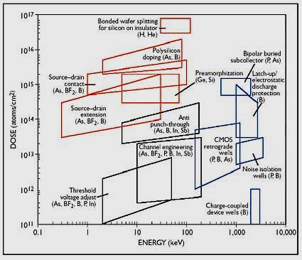
15 Dose-Energy Alication Sace 9 15
Section 6: Ion Implantation. Jaeger Chapter 5
 Section 6: Ion Imlantation Jaeger Chater 5 Ion Imlantation - Overview Wafer is Target in High Energy Accelerator Imurities Shot into Wafer Preferred Method of Adding Imurities to Wafers Wide Range of Imurity
Make sure the exam paper has 8 pages plus an appendix page at the end.
 UNIVERSITY OF CALIFORNIA College of Engineering Deartment of Electrical Engineering and Comuter Sciences Fall 2000 EE143 Midterm Exam #1 Family Name First name Signature Make sure the exam aer has 8 ages
EE 143 Microfabrication Technology Spring 2010
 EE 143 Microfabrication Technology Sring 010 Prof Clark T-C Nguyen Det of Electrical Engineering & Comuter Sciences University of California at Berkeley Berkeley, CA 9470 LecM 5 C Nguyen /14/10 1 Semiconductor
Introduction to Silvaco ATHENA Tool and Basic Concepts in Process Modeling Part - 1. Instructor: Dragica Vasileska
 Introduction to Silvaco ATHENA Tool and Basic Concets in Process Modeling Part - 1 Instructor: Dragica Vasileska Deartment of Electrical Engineering Arizona State University 1. Introduction to Process
Ion Implantation. alternative to diffusion for the introduction of dopants essentially a physical process, rather than chemical advantages:
 Ion Implantation alternative to diffusion for the introduction of dopants essentially a physical process, rather than chemical advantages: mass separation allows wide varies of dopants dose control: diffusion
Changing the Dopant Concentration. Diffusion Doping Ion Implantation
 Changing the Dopant Concentration Diffusion Doping Ion Implantation Step 11 The photoresist is removed with solvent leaving a ridge of polysilicon (the transistor's gate), which rises above the silicon
Ion Implantation ECE723
 Ion Implantation Topic covered: Process and Advantages of Ion Implantation Ion Distribution and Removal of Lattice Damage Simulation of Ion Implantation Range of Implanted Ions Ion Implantation is the
Make sure the exam paper has 7 pages (including cover page) + 3 pages of data for reference
 + 3 pages of data for reference") UNIVERSITY OF CALIFORNIA College of Engineering Department of Electrical Engineering and Computer Sciences Fall 2005 EE143 Midterm Exam #1 Family Name First name SID Signature Make sure the exam paper
UNIVERSITY OF CALIFORNIA College of Engineering Department of Electrical Engineering and Computer Sciences Fall 2005 EE143 Midterm Exam #1 Family Name First name SID Signature Make sure the exam paper
EE143 Fall 2016 Microfabrication Technologies. Lecture 6: Thin Film Deposition Reading: Jaeger Chapter 6
 EE143 Fall 2016 Microfabrication Technologies Lecture 6: Thin Film Deposition Reading: Jaeger Chapter 6 Prof. Ming C. Wu wu@eecs.berkeley.edu 511 Sutardja Dai Hall (SDH) 1 Vacuum Basics Units 1 atmosphere
EE 212 FALL ION IMPLANTATION - Chapter 8 Basic Concepts
 EE 212 FALL 1999-00 ION IMPLANTATION - Chapter 8 Basic Concepts Ion implantation is the dominant method of doping used today. In spite of creating enormous lattice damage it is favored because: Large range
Lecture 2. OUTLINE Basic Semiconductor Physics (cont d) PN Junction Diodes. Reading: Chapter Carrier drift and diffusion
 PN Junction Diodes. Reading: Chapter Carrier drift and diffusion") Lecture 2 OUTLIE Basic Semiconductor Physics (cont d) Carrier drift and diffusion P unction Diodes Electrostatics Caacitance Reading: Chater 2.1 2.2 EE105 Sring 2008 Lecture 1, 2, Slide 1 Prof. Wu, UC
Lecture 2 OUTLIE Basic Semiconductor Physics (cont d) Carrier drift and diffusion P unction Diodes Electrostatics Caacitance Reading: Chater 2.1 2.2 EE105 Sring 2008 Lecture 1, 2, Slide 1 Prof. Wu, UC
Make sure the exam paper has 9 pages (including cover page) + 3 pages of data for reference
 + 3 pages of data for reference") UNIVERSITY OF CALIFORNIA College of Engineering Department of Electrical Engineering and Computer Sciences Spring 2006 EE143 Midterm Exam #1 Family Name First name SID Signature Make sure the exam paper
UNIVERSITY OF CALIFORNIA College of Engineering Department of Electrical Engineering and Computer Sciences Spring 2006 EE143 Midterm Exam #1 Family Name First name SID Signature Make sure the exam paper
ION IMPLANTATION - Chapter 8 Basic Concepts
 ION IMPLANTATION - Chapter 8 Basic Concepts Ion implantation is the dominant method of doping used today. In spite of creating enormous lattice damage it is favored because: Large range of doses - 1 11
Ion Implant Part 1. Saroj Kumar Patra, TFE4180 Semiconductor Manufacturing Technology. Norwegian University of Science and Technology ( NTNU )
") 1 Ion Implant Part 1 Chapter 17: Semiconductor Manufacturing Technology by M. Quirk & J. Serda Spring Semester 2014 Saroj Kumar Patra,, Norwegian University of Science and Technology ( NTNU ) 2 Objectives
1 Ion Implant Part 1 Chapter 17: Semiconductor Manufacturing Technology by M. Quirk & J. Serda Spring Semester 2014 Saroj Kumar Patra,, Norwegian University of Science and Technology ( NTNU ) 2 Objectives
Lecture 5. Ion Implantation. Reading: Chapter 5
 Lecture 5 Ion Implantation Reading: Chapter 5 Shockley patented the concept of Ion Implantation for semiconductor doping in 956 ( years after Pfann patented the diffusion concept). First commercial implanters
Chapter 8 Ion Implantation
 Chapter 8 Ion Implantation 2006/5/23 1 Wafer Process Flow Materials IC Fab Metalization CMP Dielectric deposition Test Wafers Masks Thermal Processes Implant PR strip Etch PR strip Packaging Photolithography
EE143 LAB. Professor N Cheung, U.C. Berkeley
 EE143 LAB 1 1 EE143 Equipment in Cory 218 2 Guidelines for Process Integration * A sequence of Additive and Subtractive steps with lateral patterning Processing Steps Si wafer Watch out for materials compatibility
EE-612: Lecture 22: CMOS Process Steps
 EE-612: Lecture 22: CMOS Process Steps Mark Lundstrom Electrical and Computer Engineering Purdue University West Lafayette, IN USA Fall 2006 NCN www.nanohub.org Lundstrom EE-612 F06 1 outline 1) Unit Process
Processing of Semiconducting Materials Prof. Pallab Banerji Department of Metallurgy and Material Science Indian Institute of Technology, Kharagpur
 Processing of Semiconducting Materials Prof. Pallab Banerji Department of Metallurgy and Material Science Indian Institute of Technology, Kharagpur Lecture - 9 Diffusion and Ion Implantation III In my
MATHEMATICS OF DOPING PROFILES. C(x,t) t. = D 2 C(x,t) x 2. 4Dt dx '
 t. = D 2 C(x,t) x 2. 4Dt dx '") EE43 MATHEMATICS OF DOPING PROFILES N. Cheung The diffusion equation with constant D : has the general solution: C(x,t) = C(x,t) = D 2 C(x,t) 4πDt F(x ' ) e -(x-x' ) 2 4Dt dx ' - where F(x') is the C(x,t)
EE43 MATHEMATICS OF DOPING PROFILES N. Cheung The diffusion equation with constant D : has the general solution: C(x,t) = C(x,t) = D 2 C(x,t) 4πDt F(x ' ) e -(x-x' ) 2 4Dt dx ' - where F(x') is the C(x,t)
UNIVERSITY OF CALIFORNIA. College of Engineering. Department of Electrical Engineering and Computer Sciences. Professor Ali Javey.
 UNIVERSITY OF CALIFORNIA College of Engineering Department of Electrical Engineering and Computer Sciences EE 143 Professor Ali Javey Spring 2009 Exam 2 Name: SID: Closed book. One sheet of notes is allowed.
F O R SOCI AL WORK RESE ARCH
 7 TH EUROPE AN CONFERENCE F O R SOCI AL WORK RESE ARCH C h a l l e n g e s i n s o c i a l w o r k r e s e a r c h c o n f l i c t s, b a r r i e r s a n d p o s s i b i l i t i e s i n r e l a t i o n
Ion implantation Campbell, Chapter 5
 Ion implantation Campbell, Chapter 5 background why ion implant? elastic collisions nuclear and electronic stopping ion ranges: projected and lateral channeling ion-induced damage and amorphization basic
Fast Monte-Carlo Simulation of Ion Implantation. Binary Collision Approximation Implementation within ATHENA
 Fast Monte-Carlo Simulation of Ion Implantation Binary Collision Approximation Implementation within ATHENA Contents Simulation Challenges for Future Technologies Monte-Carlo Concepts and Models Atomic
ECE-305: Fall 2017 Metal Oxide Semiconductor Devices
 C-305: Fall 2017 Metal Oxide Semiconductor Devices Pierret, Semiconductor Device Fundamentals (SDF) Chapters 15+16 (pp. 525-530, 563-599) Professor Peter Bermel lectrical and Computer ngineering Purdue
VLSI Technology Dr. Nandita Dasgupta Department of Electrical Engineering Indian Institute of Technology, Madras
 VLSI Technology Dr. Nandita Dasgupta Department of Electrical Engineering Indian Institute of Technology, Madras Lecture - 20 Ion-implantation systems and damages during implantation So, in our discussion
Section 7: Diffusion. Jaeger Chapter 4. EE143 Ali Javey
 Section 7: Diffusion Jaeger Chapter 4 Surface Diffusion: Dopant Sources (a) Gas Source: AsH 3, PH 3, B 2 H 6 (b) Solid Source BN Si BN Si (c) Spin-on-glass SiO 2 +dopant oxide (d) Liquid Source. Fick s
EE105 Fall 2015 Microelectronic Devices and Circuits: Semiconductor Fabrication and PN Junctions
 EE105 Fall 2015 Microelectronic Devices and Circuits: Semiconductor Fabrication and PN Junctions Prof. Ming C. Wu wu@eecs.berkeley.edu 511 Sutardja Dai Hall (SDH) 1 pn Junction p-type semiconductor in
Properties of Error Function erf(z) And Complementary Error Function erfc(z)
 And Complementary Error Function erfc(z)") Properties of Error Function erf(z) And Complementary Error Function erfc(z) z erf (z) π e -y dy erfc (z) 1 - erf (z) erf () erf( ) 1 erf(- ) - 1 erf (z) d erf(z) dz π z for z
Properties of Error Function erf(z) And Complementary Error Function erfc(z) z erf (z) π e -y dy erfc (z) 1 - erf (z) erf () erf( ) 1 erf(- ) - 1 erf (z) d erf(z) dz π z for z
EE105 Fall 2014 Microelectronic Devices and Circuits. NMOS Transistor Capacitances: Saturation Region
 EE105 Fall 014 Microelectronic Devices and Circuits Prof. Ming C. Wu wu@eecs.berkeley.edu 511 Sutardja Dai Hall (SDH) 1 NMOS Transistor Capacitances: Saturation Region Drain no longer connected to channel
EE143 Fall 2016 Microfabrication Technologies. Evolution of Devices
 EE143 Fall 2016 Microfabrication Technologies Prof. Ming C. Wu wu@eecs.berkeley.edu 511 Sutardja Dai Hall (SDH) 1-1 Evolution of Devices Yesterday s Transistor (1947) Today s Transistor (2006) 1-2 1 Why
97.398*, Physical Electronics, Lecture 8. Diode Operation
 97.398*, Physical Electronics, Lecture 8 Diode Oeration Lecture Outline Have looked at basic diode rocessing and structures Goal is now to understand and model the behavior of the device under bias First
Modelling for Formation of Source/Drain Region by Ion Implantation and Diffusion Process for MOSFET Device
 Modelling for Formation of Source/Drain Region by Ion Implantation and Diffusion Process for MOSFET Device 1 Supratim Subhra Das 2 Ria Das 1,2 Assistant Professor, Mallabhum Institute of Technology, Bankura,
Lecture 12 Ion Implantation
 Lecture 12 Ion Implantation Chapter 9 Wolf and Tauber 1/98 Announcements Homework: Homework 3 is due at the start of class on Thursday (Nov 9 th ). Will be returned one week from Thursday (16 th Nov).
Dopant Diffusion. (1) Predeposition dopant gas. (2) Drive-in Turn off dopant gas. dose control. Doped Si region
 Predeposition dopant gas. (2) Drive-in Turn off dopant gas. dose control. Doped Si region") Dopant Diffusion (1) Predeposition dopant gas dose control SiO Si SiO Doped Si region () Drive-in Turn off dopant gas or seal surface with oxide profile control (junction depth; concentration) SiO SiO
Dopant Diffusion (1) Predeposition dopant gas dose control SiO Si SiO Doped Si region () Drive-in Turn off dopant gas or seal surface with oxide profile control (junction depth; concentration) SiO SiO
Semiconductor Integrated Process Design (MS 635)
") Semiconductor Integrated Process Design (MS 635) Instructor: Prof. Keon Jae Lee - Office: 응용공학동 #4306, Tel: #3343 - Email: keonlee@kaist.ac.kr Lecture: (Tu, Th), 1:00-2:15 #2425 Office hour: Tues & Thur
Semiconductor Integrated Process Design (MS 635) Instructor: Prof. Keon Jae Lee - Office: 응용공학동 #4306, Tel: #3343 - Email: keonlee@kaist.ac.kr Lecture: (Tu, Th), 1:00-2:15 #2425 Office hour: Tues & Thur
Motion and Recombination of Electrons and Holes
 Chater Motion and Recombination of Electrons and Holes OBJECTIVES. Understand how the electrons and holes resond to an electric field (drift).. Understand how the electrons and holes resond to a gradient
Dopant Diffusion Sources
 Dopant Diffusion (1) Predeposition dopant gas dose control SiO Si SiO Doped Si region () Drive-in Turn off dopant gas or seal surface with oide profile control (junction depth; concentration) SiO SiO Si
Chapter 9 Ion Implantation
 Chapter 9 Ion Implantation Professor Paul K. Chu Ion Implantation Ion implantation is a low-temperature technique for the introduction of impurities (dopants) into semiconductors and offers more flexibility
3.155J/6.152J Microelectronic Processing Technology Fall Term, 2004
 3.155J/6.152J Microelectronic Processing Technology Fall Term, 2004 Bob O'Handley Martin Schmidt Quiz Nov. 17, 2004 Ion implantation, diffusion [15] 1. a) Two identical p-type Si wafers (N a = 10 17 cm
EE 527 MICROFABRICATION. Lecture 24 Tai-Chang Chen University of Washington
 EE 527 MICROFABRICATION Lecture 24 Tai-Chang Chen University of Washington EDP ETCHING OF SILICON - 1 Ethylene Diamine Pyrocatechol Anisotropy: (100):(111) ~ 35:1 EDP is very corrosive, very carcinogenic,
Light element IBA by Elastic Recoil Detection and Nuclear Reaction Analysis R. Heller
 Text optional: Institute Prof. Dr. Hans Mousterian www.fzd.de Mitglied der Leibniz-Gemeinschaft Light element IBA by Elastic Recoil Detection and Nuclear Reaction Analysis R. Heller IBA Techniques slide
Lecture 150 Basic IC Processes (10/10/01) Page ECE Analog Integrated Circuits and Systems P.E. Allen
 Page ECE Analog Integrated Circuits and Systems P.E. Allen") Lecture 150 Basic IC Processes (10/10/01) Page 1501 LECTURE 150 BASIC IC PROCESSES (READING: TextSec. 2.2) INTRODUCTION Objective The objective of this presentation is: 1.) Introduce the fabrication of
Lecture 150 Basic IC Processes (10/10/01) Page 1501 LECTURE 150 BASIC IC PROCESSES (READING: TextSec. 2.2) INTRODUCTION Objective The objective of this presentation is: 1.) Introduce the fabrication of
DIFFUSION - Chapter 7
 DIFFUSION - Chapter 7 Doping profiles determine many short-channel characteristics in MOS devices. Resistance impacts drive current. Scaling implies all lateral and vertical dimensions scale by the same
Xing Sheng, 微纳光电子材料与器件工艺原理. Doping 掺杂. Xing Sheng 盛兴. Department of Electronic Engineering Tsinghua University
 微纳光电子材料与器件工艺原理 Doping 掺杂 Xing Sheng 盛兴 Department of Electronic Engineering Tsinghua University xingsheng@tsinghua.edu.cn 1 Semiconductor PN Junctions Xing Sheng, EE@Tsinghua LEDs lasers detectors solar
Evaluation of plasma strip induced substrate damage Keping Han 1, S. Luo 1, O. Escorcia 1, Carlo Waldfried 1 and Ivan Berry 1, a
 Solid State Phenomena Vols. 14-146 (29) pp 249-22 Online available since 29/Jan/6 at www.scientific.net (29) Trans Tech Publications, Switzerland doi:.428/www.scientific.net/ssp.14-146.249 Evaluation of
rate~ If no additional source of holes were present, the excess
 DIFFUSION OF CARRIERS Diffusion currents are resent in semiconductor devices which generate a satially non-uniform distribution of carriers. The most imortant examles are the -n junction and the biolar
Quiz #1 Practice Problem Set
 Name: Student Number: ELEC 3908 Physical Electronics Quiz #1 Practice Problem Set? Minutes January 22, 2016 - No aids except a non-programmable calculator - All questions must be answered - All questions
Electrochemical Society Proceedings Volume
 CALIBRATION FOR THE MONTE CARLO SIMULATION OF ION IMPLANTATION IN RELAXED SIGE Robert Wittmann, Andreas Hössinger, and Siegfried Selberherr Institute for Microelectronics, Technische Universität Wien Gusshausstr.
3.4 Design Methods for Fractional Delay Allpass Filters
 Chater 3. Fractional Delay Filters 15 3.4 Design Methods for Fractional Delay Allass Filters Above we have studied the design of FIR filters for fractional delay aroximation. ow we show how recursive or
Secondary ion mass spectrometry (SIMS)
") Secondary ion mass spectrometry (SIMS) Lasse Vines 1 Secondary ion mass spectrometry O Zn 10000 O 2 Counts/sec 1000 100 Li Na K Cr ZnO 10 ZnO 2 1 0 20 40 60 80 100 Mass (AMU) 10 21 10 20 Si 07 Ge 0.3 Atomic
Secondary ion mass spectrometry (SIMS) Lasse Vines 1 Secondary ion mass spectrometry O Zn 10000 O 2 Counts/sec 1000 100 Li Na K Cr ZnO 10 ZnO 2 1 0 20 40 60 80 100 Mass (AMU) 10 21 10 20 Si 07 Ge 0.3 Atomic
Enhancing the Efficiency of Silicon-Based Solar Cells by the
 Enhancing the Efficiency of Silicon-Based Solar Cells by the Piezo-Phototronic Effect Laian Zhu,, Longfei Wang,, Caofeng Pan, Libo Chen, Fei Xue, Baodong Chen, Leijing Yang, Li Su, and Zhong Lin Wang*,,
Ajay Kumar Gautam Asst. Prof. Electronics & Communication Engineering Dev Bhoomi Institute of Technology & Engineering Dehradun UNIT II
 Ajay Kumar Gautam Asst. Prof. Electronics & Communication Engineering Dev Bhoomi Institute of Technology & Engineering Dehradun UNIT II Syllabus EPITAXIAL PROCESS: Epitaxy and its concept, Growth kinetics
Secondary Ion Mass Spectrometry (SIMS) Thomas Sky
 Thomas Sky") 1 Secondary Ion Mass Spectrometry (SIMS) Thomas Sky Depth (µm) 2 Characterization of solar cells 0,0 1E16 1E17 1E18 1E19 1E20 0,2 0,4 0,6 0,8 1,0 1,2 P Concentration (cm -3 ) Characterization Optimization
1 Secondary Ion Mass Spectrometry (SIMS) Thomas Sky Depth (µm) 2 Characterization of solar cells 0,0 1E16 1E17 1E18 1E19 1E20 0,2 0,4 0,6 0,8 1,0 1,2 P Concentration (cm -3 ) Characterization Optimization
Optical properties of semiconductors. Dr. Katarzyna Skorupska
 Otical roerties of semiconductors Dr. Katarzyna Skoruska band structure of crystalline solids by solution of Schroedinger equation (one e - aroximation) Solution leads to energy bands searated by an energy
Thermal Oxidation of Si
 Thermal Oxidation of General Properties of O 2 Applications of thermal O 2 Deal-Grove Model of Oxidation Thermal O 2 is amorphous. Weight Density = 2.20 gm/cm 3 Molecular Density = 2.3E22 molecules/cm
An-Najah National University Civil Engineering Departemnt. Fluid Mechanics. Chapter [2] Fluid Statics
![An-Najah National University Civil Engineering Departemnt. Fluid Mechanics. Chapter [2] Fluid Statics](/thumbs/89/101171273.jpg "An-Najah National University Civil Engineering Departemnt. Fluid Mechanics. Chapter [2] Fluid Statics") An-Najah National University Civil Engineering Deartemnt Fluid Mechanics Chater [2] Fluid Statics 1 Fluid Statics Problems Fluid statics refers to the study of fluids at rest or moving in such a manner
An-Najah National University Civil Engineering Deartemnt Fluid Mechanics Chater [2] Fluid Statics 1 Fluid Statics Problems Fluid statics refers to the study of fluids at rest or moving in such a manner
MS482 Materials Characterization ( 재료분석 ) Lecture Note 5: RBS
 Lecture Note 5: RBS") 2016 Fall Semester MS482 Materials Characterization ( 재료분석 ) Lecture Note 5: RBS Byungha Shin Dept. of MSE, KAIST 1 Course Information Syllabus 1. Overview of various characterization techniques (1 lecture)
2016 Fall Semester MS482 Materials Characterization ( 재료분석 ) Lecture Note 5: RBS Byungha Shin Dept. of MSE, KAIST 1 Course Information Syllabus 1. Overview of various characterization techniques (1 lecture)
ICPMS Doherty Lecture 1
 ICPMS Doherty Lecture 1 Mass Spectrometry This material provides some background on how to measure isotope abundances by means of mass spectrometry. Mass spectrometers create and separate ionized atoms
Manufacturable AlGaAs/GaAs HBT Implant Isolation Process Using Doubly Charged Helium
 Manufacturable AlGaAs/GaAs HBT Implant Isolation Process Using Doubly Charged Helium ABSTRACT Rainier Lee, Shiban Tiku, and Wanming Sun Conexant Systems 2427 W. Hillcrest Drive Newbury Park, CA 91320 (805)
Gold Nanoparticles Floating Gate MISFET for Non-Volatile Memory Applications
 Gold Nanoparticles Floating Gate MISFET for Non-Volatile Memory Applications D. Tsoukalas, S. Kolliopoulou, P. Dimitrakis, P. Normand Institute of Microelectronics, NCSR Demokritos, Athens, Greece S. Paul,
Accelerated ions. ion doping
 30 5. Simulation of Ion Doping of Semiconductors 5.1. Objectives - To give students hand-on experience of numerical simulation of ion doping used for fabrication of semiconductor planar devices. - To familiarize
September 21, 2005, Wednesday
 , Wednesday Doping and diffusion I Faster MOSFET requires shorter channel P + Poly Al Al Motivation Requires shallower source, drain Al P + Poly Al source drain Shorter channel length; yes, but same source
Imaginary Band Structure and Its Role in Calculating Transmission Probability in Semiconductors
 Imaginary Band Structure and Its Role in Calculating Transmission Probability in Semiconductors Jamie Teherani Collaborators: Paul Solomon (IBM), Mathieu Luisier(Purdue) Advisors: Judy Hoyt, DimitriAntoniadis
Fabrication Technology, Part I
 EEL5225: Principles of MEMS Transducers (Fall 2004) Fabrication Technology, Part I Agenda: Microfabrication Overview Basic semiconductor devices Materials Key processes Oxidation Thin-film Deposition Reading:
Self-study problems and questions Processing and Device Technology, FFF110/FYSD13
 Self-study problems and questions Processing and Device Technology, FFF110/FYSD13 Version 2016_01 In addition to the problems discussed at the seminars and at the lectures, you can use this set of problems
Lecture 24. Ideal Gas Law and Kinetic Theory
 Lecture 4 Ideal Gas Law and Kinetic Theory Today s Topics: Ideal Gas Law Kinetic Theory of Gases Phase equilibria and phase diagrams Ideal Gas Law An ideal gas is an idealized model for real gases that
Diffusion. Diffusion = the spontaneous intermingling of the particles of two or more substances as a result of random thermal motion
 Diffusion Diffusion = the spontaneous intermingling of the particles of two or more substances as a result of random thermal motion Fick s First Law Γ ΔN AΔt Γ = flux ΔN = number of particles crossing
EE105 Fall 2014 Microelectronic Devices and Circuits
 EE05 Fall 204 Microelectronic Devices and Circuits Prof. Ming C. Wu wu@eecs.berkeley.edu 5 Sutardja Dai Hall (SDH) Terminal Gain and I/O Resistances of BJT Amplifiers Emitter (CE) Collector (CC) Base (CB)
Solid State Device Fundamentals
 Solid State Device Fundamentals ENS 345 Lecture Course by Alexander M. Zaitsev alexander.zaitsev@csi.cuny.edu Tel: 718 982 2812 Office 4N101b 1 Outline - Goals of the course. What is electronic device?
Chapter 3 Engineering Science for Microsystems Design and Fabrication
 Lectures on MEMS and MICROSYSTEMS DESIGN and MANUFACTURE Chapter 3 Engineering Science for Microsystems Design and Fabrication In this Chapter, we will present overviews of the principles of physical and
Diffusion and Ion implantation Reference: Chapter 4 Jaeger or Chapter 3 Ruska N & P Dopants determine the resistivity of material Note N lower
 Diffusion and Ion implantation Reference: Chapter 4 Jaeger or Chapter 3 Ruska N & P Dopants determine the resistivity of material Note N lower resistavity than p: due to higher carrier mobility Near linear
EE 434 Lecture 12. Process Flow (wrap up) Device Modeling in Semiconductor Processes
 Device Modeling in Semiconductor Processes") EE 434 Lecture 12 Process Flow (wrap up) Device Modeling in Semiconductor Processes Quiz 6 How have process engineers configured a process to assure that the thickness of the gate oxide for the p-channel
EE 434 Lecture 12 Process Flow (wrap up) Device Modeling in Semiconductor Processes Quiz 6 How have process engineers configured a process to assure that the thickness of the gate oxide for the p-channel
International Association of Scientific Innovation and Research (IASIR) (An Association Unifying the Sciences, Engineering, and Applied Research)
 (An Association Unifying the Sciences, Engineering, and Applied Research)") International Association of ientific Innovation and Research (IASIR) (An Association Unifying the iences, Engineering, and Alied Research) International Journal of Emerging Technologies in Comutational
International Association of ientific Innovation and Research (IASIR) (An Association Unifying the iences, Engineering, and Alied Research) International Journal of Emerging Technologies in Comutational
CHAPTER 2 Fluid Statics
 Chater / Fluid Statics CHAPTER Fluid Statics FE-tye Exam Review Problems: Problems - to -9. (C) h (.6 98) (8.5.54) 96 6 Pa Hg. (D) gh 84. 9.8 4 44 76 Pa. (C) h h. 98. 8 Pa w atm x x water w.4 (A) H (.6
Solid State Device Fundamentals
 Solid State Device Fundamentals ENS 345 Lecture Course by Alexander M. Zaitsev alexander.zaitsev@csi.cuny.edu Tel: 718 982 2812 Office 4N101b 1 Outline - Goals of the course. What is electronic device?
MS482 Materials Characterization ( 재료분석 ) Lecture Note 5: RBS. Byungha Shin Dept. of MSE, KAIST
 Lecture Note 5: RBS. Byungha Shin Dept. of MSE, KAIST") 2015 Fall Semester MS482 Materials Characterization ( 재료분석 ) Lecture Note 5: RBS Byungha Shin Dept. of MSE, KAIST 1 Course Information Syllabus 1. Overview of various characterization techniques (1 lecture)
2015 Fall Semester MS482 Materials Characterization ( 재료분석 ) Lecture Note 5: RBS Byungha Shin Dept. of MSE, KAIST 1 Course Information Syllabus 1. Overview of various characterization techniques (1 lecture)
ECE-305: Fall 2017 MOS Capacitors and Transistors
 ECE-305: Fall 2017 MOS Capacitors and Transistors Pierret, Semiconductor Device Fundamentals (SDF) Chapters 15+16 (pp. 525-530, 563-599) Professor Peter Bermel Electrical and Computer Engineering Purdue
EE 508 Lecture 13. Statistical Characterization of Filter Characteristics
 EE 508 Lecture 3 Statistical Characterization of Filter Characteristics Comonents used to build filters are not recisely redictable L C Temerature Variations Manufacturing Variations Aging Model variations
Lab1. Resolution and Throughput of Ion Beam Lithography.
 1 ENS/PHY463 Lab1. Resolution and Throughput of Ion Beam Lithography. (SRIM 2008/2013 computer simulation) Objective The objective of this laboratory work is to evaluate the exposure depth, resolution,
CHAPTER 2 Fluid Statics
 Chater / Fluid Statics CHAPTER Fluid Statics FE-tye Exam Review Problems: Problems - to -9. (C) h (.6 98) (8.5.54) 96 6 Pa Hg. (D) gh 84. 9.8 4 44 76 Pa. (C) h h. 98. 8 Pa w atm x x water w.4 (A) H (.6
T i t l e o f t h e w o r k : L a M a r e a Y o k o h a m a. A r t i s t : M a r i a n o P e n s o t t i ( P l a y w r i g h t, D i r e c t o r )
") v e r. E N G O u t l i n e T i t l e o f t h e w o r k : L a M a r e a Y o k o h a m a A r t i s t : M a r i a n o P e n s o t t i ( P l a y w r i g h t, D i r e c t o r ) C o n t e n t s : T h i s w o
v e r. E N G O u t l i n e T i t l e o f t h e w o r k : L a M a r e a Y o k o h a m a A r t i s t : M a r i a n o P e n s o t t i ( P l a y w r i g h t, D i r e c t o r ) C o n t e n t s : T h i s w o
Chapter 8 Ion Implantation
 Chapter 8 Ion Implantation Hong Xiao, Ph. D. hxiao89@hotmail.com www2.austin.cc.tx.us/hongxiao/book.htm Hong Xiao, Ph. D. www2.austin.cc.tx.us/hongxiao/book.htm 1 Objectives List at least three commonly
 ! " # $! % & '! , ) ( + - (. ) ( ) * + / 0 1 2 3 0 / 4 5 / 6 0 ; 8 7 < = 7 > 8 7 8 9 : Œ Š ž P P h ˆ Š ˆ Œ ˆ Š ˆ Ž Ž Ý Ü Ý Ü Ý Ž Ý ê ç è ± ¹ ¼ ¹ ä ± ¹ w ç ¹ è ¼ è Œ ¹ ± ¹ è ¹ è ä ç w ¹ ã ¼ ¹ ä ¹ ¼ ¹ ±
ESE 570: Digital Integrated Circuits and VLSI Fundamentals
 ESE 570: Digital Integrated Circuits and VLSI Fundamentals Lec 4: January 29, 2019 MOS Transistor Theory, MOS Model Penn ESE 570 Spring 2019 Khanna Lecture Outline! CMOS Process Enhancements! Semiconductor
Auger Electron Spectroscopy (AES) Prof. Paul K. Chu
 Prof. Paul K. Chu") Auger Electron Spectroscopy (AES) Prof. Paul K. Chu Auger Electron Spectroscopy Introduction Principles Instrumentation Qualitative analysis Quantitative analysis Depth profiling Mapping Examples The Auger
Auger Electron Spectroscopy (AES) Prof. Paul K. Chu Auger Electron Spectroscopy Introduction Principles Instrumentation Qualitative analysis Quantitative analysis Depth profiling Mapping Examples The Auger
ESE 570: Digital Integrated Circuits and VLSI Fundamentals
 ESE 570: Digital Integrated Circuits and VLSI Fundamentals Lec 4: January 23, 2018 MOS Transistor Theory, MOS Model Penn ESE 570 Spring 2018 Khanna Lecture Outline! CMOS Process Enhancements! Semiconductor
Chapter 2 Instrumentation for Analytical Electron Microscopy Lecture 5. Chapter 2 CHEM 793, 2011 Fall 1
 Chater Instrumentation for Analytical Electron Microscoy Lecture 5 Chater CHEM 793, 011 Fall 1 Outline Electron Sources (Electron Guns) Thermionic: LaB 6 or W Field emission gun: cold or Schottky Lenses
EE 434 Lecture 13. Basic Semiconductor Processes Devices in Semiconductor Processes
 EE 434 Lecture 3 Basic Semiconductor Processes Devices in Semiconductor Processes Quiz 9 The top view of a device fabricated in a bulk CMOS process is shown in the figure below a) Identify the device b)
MENA9510 characterization course: Capacitance-voltage (CV) measurements
 measurements") MENA9510 characterization course: Capacitance-voltage (CV) measurements 30.10.2017 Halvard Haug Outline Overview of interesting sample structures Ohmic and schottky contacts Why C-V for solar cells? The
MENA9510 characterization course: Capacitance-voltage (CV) measurements 30.10.2017 Halvard Haug Outline Overview of interesting sample structures Ohmic and schottky contacts Why C-V for solar cells? The
FLCC Seminar. Spacer Lithography for Reduced Variability in MOSFET Performance
 1 Seminar Spacer Lithography for Reduced Variability in MOSFET Performance Prof. Tsu-Jae King Liu Electrical Engineering & Computer Sciences Dept. University of California at Berkeley Graduate Student:
Limits and Continuity. 2 lim. x x x 3. lim x. lim. sinq. 5. Find the horizontal asymptote (s) of. Summer Packet AP Calculus BC Page 4
 of. Summer Packet AP Calculus BC Page 4") Limits and Continuity t+ 1. lim t - t + 4. lim x x x x + - 9-18 x-. lim x 0 4-x- x 4. sinq lim - q q 5. Find the horizontal asymptote (s) of 7x-18 f ( x) = x+ 8 Summer Packet AP Calculus BC Page 4 6. x
Limits and Continuity t+ 1. lim t - t + 4. lim x x x x + - 9-18 x-. lim x 0 4-x- x 4. sinq lim - q q 5. Find the horizontal asymptote (s) of 7x-18 f ( x) = x+ 8 Summer Packet AP Calculus BC Page 4 6. x
Lecture 6 Plasmas. Chapters 10 &16 Wolf and Tauber. ECE611 / CHE611 Electronic Materials Processing Fall John Labram 1/68
 Lecture 6 Plasmas Chapters 10 &16 Wolf and Tauber 1/68 Announcements Homework: Homework will be returned to you on Thursday (12 th October). Solutions will be also posted online on Thursday (12 th October)
ELEN0037 Microelectronic IC Design. Prof. Dr. Michael Kraft
 ELEN0037 Microelectronic IC Design Prof. Dr. Michael Kraft Lecture 2: Technological Aspects Technology Passive components Active components CMOS Process Basic Layout Scaling CMOS Technology Integrated
Section 12: Intro to Devices
 Section 12: Intro to Devices Extensive reading materials on reserve, including Robert F. Pierret, Semiconductor Device Fundamentals Bond Model of Electrons and Holes Si Si Si Si Si Si Si Si Si Silicon
EE 508 Lecture 13. Statistical Characterization of Filter Characteristics
 EE 508 Lecture 3 Statistical Characterization of Filter Characteristics Comonents used to build filters are not recisely redictable R L C Temerature Variations Manufacturing Variations Aging Model variations
= 1 3. r in. dr in. 6 dt = 1 2 A in. dt = 3 ds
 . B. Consider the octagon slit u into eight isosceles triangles with vertex angle o and base angles o /. We want to calculate the aothem using the tangent half-angle formula and a right triangle with base
ABSTRACT I NTRODUCT ION
 DESIGN OF AN ION IMPLANTATION PROCESS MONITORING CHIP ON I.C.E. AND PROVIDE A METHODOLOGY FOR EVALUATION OF TESTING RESULTS. by JOSEPH J. BURKIS 5th YEAR MiCROELECTRONIC STUDENT ROCHESTER INSTITUTE OF
DEPOSITION OF THIN TiO 2 FILMS BY DC MAGNETRON SPUTTERING METHOD
 Chapter 4 DEPOSITION OF THIN TiO 2 FILMS BY DC MAGNETRON SPUTTERING METHOD 4.1 INTRODUCTION Sputter deposition process is another old technique being used in modern semiconductor industries. Sputtering
Secondary Ion Mass Spectrometry (SIMS)
") CHEM53200: Lecture 10 Secondary Ion Mass Spectrometry (SIMS) Major reference: Surface Analysis Edited by J. C. Vickerman (1997). 1 Primary particles may be: Secondary particles can be e s, neutral species
CHEM53200: Lecture 10 Secondary Ion Mass Spectrometry (SIMS) Major reference: Surface Analysis Edited by J. C. Vickerman (1997). 1 Primary particles may be: Secondary particles can be e s, neutral species