Modeling and Analysis of Full-Chip Parasitic Substrate Currents
|
|
|
- Randolph Quinn
- 5 years ago
- Views:
Transcription


1 Modeling and Analysis of Full-Chip Parasitic Substrate Currents R. Gillon, W. Schoenmaker September 11, 2017 Rev
2 Outline Objectives Challenges SPX solver Solutions l Compact Modeling (ONSEMI) l Quasi-neutral Region Model: 1D case l The AUTOMICS Approach (EPFL/MC univ) l TCAD-inspired (MAGWEL) 2
3 Objective : Full Chip Substrate Simulation Latch-up is a prominent risk in HV processes The methodology prescribes passing LU tests Today only empirical guidelines and DRC rules are available to help designers reduce this risk Parasitic bipolars challenge the isolation High-impedance nodes pick-up unwanted signals The traditional approach with parasitic BJT models fails ( layout dependency of the β gain ) There is a need for a layout-based tool simulating carrier transport at full-chip level 3
4 The challenge Typical smart-power IC contains 100+ pockets and 10+ power domains Standard TCAD tools require sub-μm meshing (~ 10nm) and can not cope with chip complexity and dimensions Simulation of carrier transport effects at the full-chip level requires simplifications: Apply a divide and conquer approach (sub-domains) Replace the (TCAD) equations set to be solved by simplified and compact versions (approximations) 4

5 Classical BJT Concepts Not Suitable The current gain β is not invariant with respect to boundary conditions Consider two N-type tubs on a P substrate Bias one as an injector, the other as a collector The current gain varies depending on the presence of additional collectors 5
6 Full-chip LU Sims : more than just TCAD Target usage : Find weak spots for LU or parasitic BJT coupling Let the designer home-in and solve them Interaction of circuit and substrate to be simulated Modalities : Co-simulation: too complex and slow excluded! Annotation of schematics with substrate models Need for a new multi-terminal model for carrier transport in the substrate The substrate is inherently multi-emitter/collector and can not be reduced to simple BJT models 6


7 Solutions : 1 Divide and Conquer Introduce dual-carrier ports allowing to : Split the chip in quasi-neutral regions Handle depletion regions as boundary conditions Reconstruct an abstract model of the substrate with carrier transport in the circuit simulator 7
8 Solutions : 2 Reduced Equations Set Full Set for Carrier Transport in a Semiconductor E = V ϵsi. E =q( p n N A +N D ) J n=qμ n n E +q Dn n J p =qμ p p E q D p p 1 t n. J n = R( p,n) q 1 t p+. J p = R( p,n) q E = V ϵsi. E =0 J n=qμ n n E +q Dn n { transport } J p =q μ p p E q D p p 1. J n =R( p, n) { current continuity } q 1. J p= R (p, n) q { electric } Coupled system of equations Iterative solution strategy Junctions simulated in detail Simplified Set for Quasi-Neutral Regions Depletion regions domain Steady-state only Solution in single forward pass (Decoupled' system) Junctions are boundary conditions 8
 Any solution is a linear combination of Quasi-Fermi level differences total excess carrier densities at the ports Excess profiles for electron and holes coincide An internal electric")
9 Quasi-neutral Region Model : 1D Case Basic QNR resistor Zero applied E-field Canonical solution of the 1D equations : δ n=δ p= A ±. exp(±x / L DA ) Any solution is a linear combination of Quasi-Fermi level differences total excess carrier densities at the ports Excess profiles for electron and holes coincide An internal electric field equalizes the gradients ( ambipolar diffusion) Jn and Jp are exactly opposite 9
=0 δ n ( x")

10 Quasi-neutral Region Model : 1D Case As the base of a BJT A+ is positive A_ is negative n ( x 2 )=0 δ n ( x 2)= n0 A small electric field must compensate the majority diffusion currents at the edges of the depletion regions 10


11 Applications of the QNR Resistor Model For metallic contacts For P/N diodes (*) For arbitrary structures : Crossing makes a junction straight for same type Possibility to mesh using 1D elements (*) models valid in moderate till the onset of high injection 11
12 Generalization to the Multi-port Case Key principles: Use linear combinations of diode-mode solutions Characterize diode modes using transfer coefficients δ ni α ij = J n (P i)=j p (P i)=0 δnj Build carrier-balance equations to determine Aj F (U Fn (Pi) U Fp (Pi ))= j α ij A j Diffusion currents J diff =±qd Drift currents d δc =±qd δ c (Pi )/ LDA dz J drift (i)= j Y ij (V j V Dmbj ) 12 c= p, n

13 Basic Claim of the QNR Mesh Model The complete carrier transport behavior of a multiterminal bipolar can be reconstructed from diodemode characteristics only! Diode-mode characterization Bipolar-mode operation 13


14 MAGWEL s SPX Solver -TCAD inspired Simulation Flow Geometry from GDS Layers in tech file 3D structure with substrate and ports DOE for DC bias Analyze distributions Quasi-Fermi level Densities Current, Solver s Strategy Solve for equilibrium Solve Poisson field only one(!) per bias Replace junctions by boundary conditions Solve minority flow Solver majority flow Check solution quality Typically 3 mins per bias point Sweeping all diodes in 24 hours 14

15 Top view of the structure p-tap 0V C3 floating p-tap 0V p-tap 0V E1 0 to -2V C4 floating p-tap 0V p-tap 0V p-tap 0V C2 10V 57 mu p-tap 0V 15

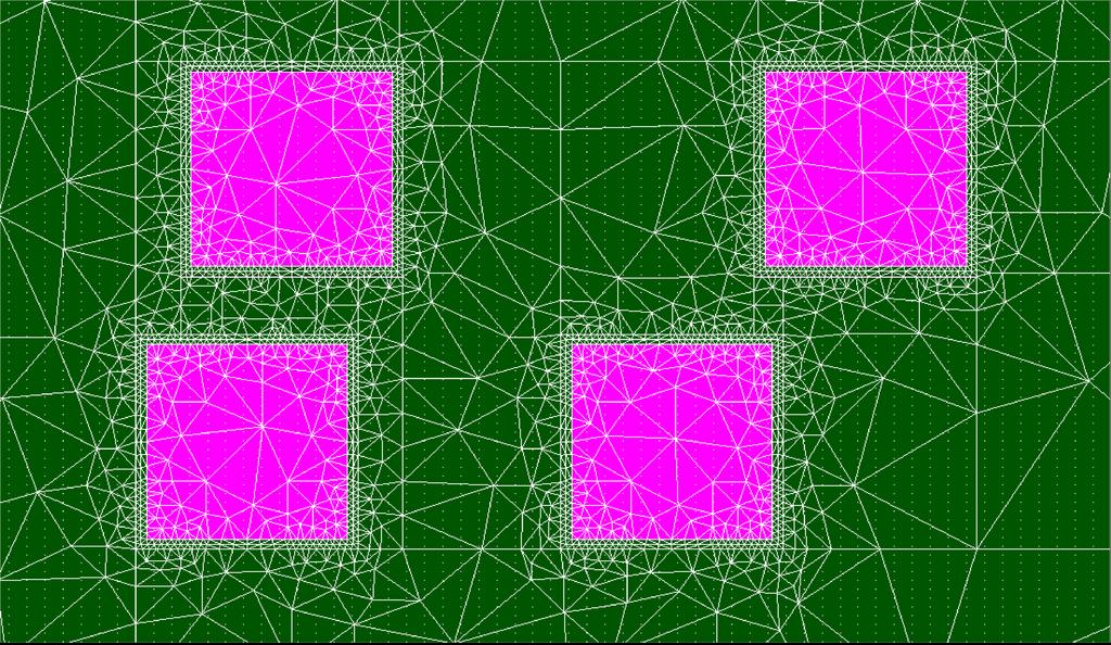
16 Some mesh details (SPX) 16


17 Excess electron density Z=310 mu Z=320 mu Z=330 mu y is constant and x through center E1 and C2 17
18 Excess electron density y is constant and x through center C3 and C4 18


19 Severe meshing demands! 19
 A 3D mesh of QNR")

20 The AUTOMICS Approach Pioneered at EPFL, tested at AMS and STM l Commercialized by PN Solutions (spin-off P&M Curie /EPFL ) A 3D mesh of QNR resistors One wire for total current One wire for minority carriers gradient Models junctions, dynamic effects, breakdown Drawback : 3D mesh solved in circuit simulator 20
21 The Infineon / Univ. Hannover Approach Ports with wires for carrier densities and electric potential Carrier transport in the substrate modeled by fitting functions to TCAD simulations VerilogA model computes distribution of carriers Drawback : standard TCAD solver not optimized for QNR 21
 Bipolar operation :")
22 Validating the QNR Mesh Claim I3T80 test-chip 4x 70x70μm² pockets + 1 long subs. contact Diode-mode biasing : One pocket biased negatively wrt to substrate Other pockets floating (zero total current) Bipolar operation : Single collectors Multiple collectors Multiple emitters
23 Model Built for the Test-structure Several QNRRes instances for the pockets One QNRMesh instance for the substrate 23
24 Model Validation : Diode-mode Comparison of floating pocket voltages Model s extracted from SPX simulations 24
25 Model Validation : Bipolar Mode Comparing SPX and circuit model to measured data 1 emitter, 3 collectors, model extracted from diode mode, no fitting Residues are the errors in measured and SPX simulated balances 25
26 Model Validation : More Bipolar Mode Comparing SPX and circuit model to measured data 1 emitter, 3 collectors, model extracted from diode mode, no fitting 26
27 Implications of the QNR Mesh Results Diode-mode characterization : Linear in the number of ports : Sweep one diode and collect s (no need to measure interactions) Faster n-port characterization with FEM tool Carrier injection efficiencies : Find risky aggressor victim pairs by inspection for high-injection effects 27
28 Summary Modeling is done as: Substrate block acts as a transport vehicle for carriers l Resistive network l Mesh-based network (SPX) Carriers are injected and collected with compact-model models representing biased pockets l Analytic compact models l Numerical compact models (SPX) 28
29 Conclusions The dual-carrier framework and the superposition of diode-mode solutions are proven to work well for building substrate models A 2-port model and a multi-port generalization were generated and validated EEPO (OnSemi) is building a complete flow based on FEM calibration of compact substrate models Future work : Scaling to more than 1000 ports (multi-pole methods) AC and transient behavior More physical collector models (velocity saturation) 29 29
30 Time for Questions! 30
DC and AC modeling of minority carriers currents in ICs substrate
 DC and AC modeling of minority carriers currents in ICs substrate Camillo Stefanucci, Pietro Buccella, Maher Kayal and Jean-Michel Sallese Swiss Federal Institute of Technology Lausanne, Switzerland MOS-AK
Semiconductor Physics and Devices
 The pn Junction 1) Charge carriers crossing the junction. 3) Barrier potential Semiconductor Physics and Devices Chapter 8. The pn Junction Diode 2) Formation of positive and negative ions. 4) Formation
Lecture 15 - The pn Junction Diode (I) I-V Characteristics. November 1, 2005
 I-V Characteristics. November 1, 2005") 6.012 - Microelectronic Devices and Circuits - Fall 2005 Lecture 15-1 Lecture 15 - The pn Junction Diode (I) I-V Characteristics November 1, 2005 Contents: 1. pn junction under bias 2. I-V characteristics
6.012 - Microelectronic Devices and Circuits - Fall 2005 Lecture 15-1 Lecture 15 - The pn Junction Diode (I) I-V Characteristics November 1, 2005 Contents: 1. pn junction under bias 2. I-V characteristics
EE105 - Fall 2006 Microelectronic Devices and Circuits
 EE105 - Fall 2006 Microelectronic Devices and Circuits Prof. Jan M. Rabaey (jan@eecs) Lecture 21: Bipolar Junction Transistor Administrative Midterm Th 6:30-8pm in Sibley Auditorium Covering everything
Session 6: Solid State Physics. Diode
 Session 6: Solid State Physics Diode 1 Outline A B C D E F G H I J 2 Definitions / Assumptions Homojunction: the junction is between two regions of the same material Heterojunction: the junction is between
Semiconductor Physics. Lecture 6
 Semiconductor Physics Lecture 6 Recap pn junction and the depletion region Driven by the need to have no gradient in the fermi level free carriers migrate across the pn junction leaving a region with few
Final Examination EE 130 December 16, 1997 Time allotted: 180 minutes
 Final Examination EE 130 December 16, 1997 Time allotted: 180 minutes Problem 1: Semiconductor Fundamentals [30 points] A uniformly doped silicon sample of length 100µm and cross-sectional area 100µm 2
ELEC 3908, Physical Electronics, Lecture 17. Bipolar Transistor Injection Models
 LC 3908, Physical lectronics, Lecture 17 Bipolar Transistor njection Models Lecture Outline Last lecture looked at qualitative operation of the BJT, now want to develop a quantitative model to predict
Current mechanisms Exam January 27, 2012
 Current mechanisms Exam January 27, 2012 There are four mechanisms that typically cause currents to flow: thermionic emission, diffusion, drift, and tunneling. Explain briefly which kind of current mechanisms
Lecture 19 - p-n Junction (cont.) October 18, Ideal p-n junction out of equilibrium (cont.) 2. pn junction diode: parasitics, dynamics
 October 18, Ideal p-n junction out of equilibrium (cont.) 2. pn junction diode: parasitics, dynamics") 6.720J/3.43J - Integrated Microelectronic Devices - Fall 2002 Lecture 19-1 Lecture 19 - p-n Junction (cont.) October 18, 2002 Contents: 1. Ideal p-n junction out of equilibrium (cont.) 2. pn junction diode:
6.720J/3.43J - Integrated Microelectronic Devices - Fall 2002 Lecture 19-1 Lecture 19 - p-n Junction (cont.) October 18, 2002 Contents: 1. Ideal p-n junction out of equilibrium (cont.) 2. pn junction diode:
BJT - Mode of Operations
 JT - Mode of Operations JTs can be modeled by two back-to-back diodes. N+ P N- N+ JTs are operated in four modes. HO #6: LN 251 - JT M Models Page 1 1) Forward active / normal junction forward biased junction
Lecture 16 - The pn Junction Diode (II) Equivalent Circuit Model. April 8, 2003
 Equivalent Circuit Model. April 8, 2003") 6.012 - Microelectronic Devices and Circuits - Spring 2003 Lecture 16-1 Lecture 16 - The pn Junction Diode (II) Equivalent Circuit Model April 8, 2003 Contents: 1. I-V characteristics (cont.) 2. Small-signal
6.012 - Microelectronic Devices and Circuits - Spring 2003 Lecture 16-1 Lecture 16 - The pn Junction Diode (II) Equivalent Circuit Model April 8, 2003 Contents: 1. I-V characteristics (cont.) 2. Small-signal
Lecture 17. The Bipolar Junction Transistor (II) Regimes of Operation. Outline
 Regimes of Operation. Outline") Lecture 17 The Bipolar Junction Transistor (II) Regimes of Operation Outline Regimes of operation Large-signal equivalent circuit model Output characteristics Reading Assignment: Howe and Sodini; Chapter
Lecture 17 The Bipolar Junction Transistor (II) Regimes of Operation Outline Regimes of operation Large-signal equivalent circuit model Output characteristics Reading Assignment: Howe and Sodini; Chapter
Lecture 16 The pn Junction Diode (III)
") Lecture 16 The pn Junction iode (III) Outline I V Characteristics (Review) Small signal equivalent circuit model Carrier charge storage iffusion capacitance Reading Assignment: Howe and Sodini; Chapter
Lecture 16 The pn Junction iode (III) Outline I V Characteristics (Review) Small signal equivalent circuit model Carrier charge storage iffusion capacitance Reading Assignment: Howe and Sodini; Chapter
Semiconductor Physics fall 2012 problems
 Semiconductor Physics fall 2012 problems 1. An n-type sample of silicon has a uniform density N D = 10 16 atoms cm -3 of arsenic, and a p-type silicon sample has N A = 10 15 atoms cm -3 of boron. For each
Diodes. anode. cathode. cut-off. Can be approximated by a piecewise-linear-like characteristic. Lecture 9-1
 Diodes mplest nonlinear circuit element Basic operation sets the foundation for Bipolar Junction Transistors (BJTs) Also present in Field Effect Transistors (FETs) Ideal diode characteristic anode cathode
Semiconductor Junctions
 8 Semiconductor Junctions Almost all solar cells contain junctions between different materials of different doping. Since these junctions are crucial to the operation of the solar cell, we will discuss
Semiconductor Physics fall 2012 problems
 Semiconductor Physics fall 2012 problems 1. An n-type sample of silicon has a uniform density N D = 10 16 atoms cm -3 of arsenic, and a p-type silicon sample has N A = 10 15 atoms cm -3 of boron. For each
Recitation 17: BJT-Basic Operation in FAR
 Recitation 17: BJT-Basic Operation in FAR BJT stands for Bipolar Junction Transistor 1. Can be thought of as two p-n junctions back to back, you can have pnp or npn. In analogy to MOSFET small current
ELEC 3908, Physical Electronics, Lecture 18. The Early Effect, Breakdown and Self-Heating
 ELEC 3908, Physical Electronics, Lecture 18 The Early Effect, Breakdown and Self-Heating Lecture Outline Previous 2 lectures analyzed fundamental static (dc) carrier transport in the bipolar transistor
6.012 Electronic Devices and Circuits
 Page 1 of 1 YOUR NAME Department of Electrical Engineering and Computer Science Massachusetts Institute of Technology 6.12 Electronic Devices and Circuits Exam No. 1 Wednesday, October 7, 29 7:3 to 9:3
p-n junction biasing, p-n I-V characteristics, p-n currents Norlaili Mohd. Noh EEE /09
 CLASS 6&7 p-n junction biasing, p-n I-V characteristics, p-n currents 1 p-n junction biasing Unbiased p-n junction: the potential barrier is 0.7 V for Si and 0.3 V for Ge. Nett current across the p-n junction
Chapter 7. The pn Junction
 Chapter 7 The pn Junction Chapter 7 PN Junction PN junction can be fabricated by implanting or diffusing donors into a P-type substrate such that a layer of semiconductor is converted into N type. Converting
Spring Semester 2012 Final Exam
 Spring Semester 2012 Final Exam Note: Show your work, underline results, and always show units. Official exam time: 2.0 hours; an extension of at least 1.0 hour will be granted to anyone. Materials parameters
Semiconductor Physics Problems 2015
 Semiconductor Physics Problems 2015 Page and figure numbers refer to Semiconductor Devices Physics and Technology, 3rd edition, by SM Sze and M-K Lee 1. The purest semiconductor crystals it is possible
Device Physics: The Bipolar Transistor
 Monolithic Amplifier Circuits: Device Physics: The Bipolar Transistor Chapter 4 Jón Tómas Guðmundsson tumi@hi.is 2. Week Fall 2010 1 Introduction In analog design the transistors are not simply switches
Lecture 17 - The Bipolar Junction Transistor (I) Forward Active Regime. April 10, 2003
 Forward Active Regime. April 10, 2003") 6.012 - Microelectronic Devices and Circuits - Spring 2003 Lecture 17-1 Lecture 17 - The Bipolar Junction Transistor (I) Contents: Forward Active Regime April 10, 2003 1. BJT: structure and basic operation
6.012 - Microelectronic Devices and Circuits - Spring 2003 Lecture 17-1 Lecture 17 - The Bipolar Junction Transistor (I) Contents: Forward Active Regime April 10, 2003 1. BJT: structure and basic operation
Forward-Active Terminal Currents
 Forward-Active Terminal Currents Collector current: (electron diffusion current density) x (emitter area) diff J n AE qd n n po A E V E V th ------------------------------ e W (why minus sign? is by def.
ECE-305: Spring 2018 Exam 2 Review
 ECE-305: Spring 018 Exam Review Pierret, Semiconductor Device Fundamentals (SDF) Chapter 3 (pp. 75-138) Chapter 5 (pp. 195-6) Professor Peter Bermel Electrical and Computer Engineering Purdue University,
Lecture 15 The pn Junction Diode (II)
") Lecture 15 The pn Junction Diode (II I-V characteristics Forward Bias Reverse Bias Outline Reading Assignment: Howe and Sodini; Chapter 6, Sections 6.4-6.5 6.012 Spring 2007 Lecture 15 1 1. I-V Characteristics
Lecture 15 The pn Junction Diode (II I-V characteristics Forward Bias Reverse Bias Outline Reading Assignment: Howe and Sodini; Chapter 6, Sections 6.4-6.5 6.012 Spring 2007 Lecture 15 1 1. I-V Characteristics
Solid State Electronics. Final Examination
 The University of Toledo EECS:4400/5400/7400 Solid State Electronic Section elssf08fs.fm - 1 Solid State Electronics Final Examination Problems Points 1. 1. 14 3. 14 Total 40 Was the exam fair? yes no
Electronic Devices and Circuits Lecture 5 - p-n Junction Injection and Flow - Outline
 6.012 - Electronic Devices and Circuits Lecture 5 - p-n Junction Injection and Flow - Outline Review Depletion approimation for an abrupt p-n junction Depletion charge storage and depletion capacitance
ECE 340 Lecture 21 : P-N Junction II Class Outline:
 ECE 340 Lecture 21 : P-N Junction II Class Outline: Contact Potential Equilibrium Fermi Levels Things you should know when you leave Key Questions What is the contact potential? Where does the transition
( )! N D ( x) ) and equilibrium
! N D ( x) ) and equilibrium") ECE 66: SOLUTIONS: ECE 66 Homework Week 8 Mark Lundstrom March 7, 13 1) The doping profile for an n- type silicon wafer ( N D = 1 15 cm - 3 ) with a heavily doped thin layer at the surface (surface concentration,
ECE 66: SOLUTIONS: ECE 66 Homework Week 8 Mark Lundstrom March 7, 13 1) The doping profile for an n- type silicon wafer ( N D = 1 15 cm - 3 ) with a heavily doped thin layer at the surface (surface concentration,
R. Ludwig and G. Bogdanov RF Circuit Design: Theory and Applications 2 nd edition. Figures for Chapter 6
 R. Ludwig and G. Bogdanov RF Circuit Design: Theory and Applications 2 nd edition Figures for Chapter 6 Free electron Conduction band Hole W g W C Forbidden Band or Bandgap W V Electron energy Hole Valence
This is the 15th lecture of this course in which we begin a new topic, Excess Carriers. This topic will be covered in two lectures.
 Solid State Devices Dr. S. Karmalkar Department of Electronics and Communication Engineering Indian Institute of Technology, Madras Lecture - 15 Excess Carriers This is the 15th lecture of this course
Bipolar Transistor WS 2011
 Institut für Integrierte Systeme Integrated Systems Laboratory Bipolar Transistor WS 2011 1 Introduction In this exercise we want to simulate the IV characteristics of a bipolar transistor and draw the
B12: Semiconductor Devices
 B12: Semiconductor Devices Example Sheet 2: Solutions Question 1 To get from eq. (5.70) of the notes to the expression given in the examples sheet, we simply invoke the relations n 0 p 0, n 0 n 0. In this
SOLUTIONS: ECE 606 Homework Week 10 Mark Lundstrom. Purdue University. (Revised 3/29/13)
") ECE- 66 SOLUTIOS: ECE 66 Homework Week 1 Mark Lundstrom (Revised 3/9/13) 1) In a forward- biased P junction under low- injection conditions, the QFL s are aroximately flat from the majority carrier region
ECE- 66 SOLUTIOS: ECE 66 Homework Week 1 Mark Lundstrom (Revised 3/9/13) 1) In a forward- biased P junction under low- injection conditions, the QFL s are aroximately flat from the majority carrier region
Lecture 35 - Bipolar Junction Transistor (cont.) November 27, Current-voltage characteristics of ideal BJT (cont.)
 November 27, Current-voltage characteristics of ideal BJT (cont.)") 6.720J/3.43J - Integrated Microelectronic Devices - Fall 2002 Lecture 35-1 Lecture 35 - Bipolar Junction Transistor (cont.) November 27, 2002 Contents: 1. Current-voltage characteristics of ideal BJT (cont.)
6.720J/3.43J - Integrated Microelectronic Devices - Fall 2002 Lecture 35-1 Lecture 35 - Bipolar Junction Transistor (cont.) November 27, 2002 Contents: 1. Current-voltage characteristics of ideal BJT (cont.)
ELECTRONICS IA 2017 SCHEME
 ELECTRONICS IA 2017 SCHEME CONTENTS 1 [ 5 marks ]...4 2...5 a. [ 2 marks ]...5 b. [ 2 marks ]...5 c. [ 5 marks ]...5 d. [ 2 marks ]...5 3...6 a. [ 3 marks ]...6 b. [ 3 marks ]...6 4 [ 7 marks ]...7 5...8
EE 3329 Electronic Devices Syllabus ( Extended Play )
") EE 3329 - Electronic Devices Syllabus EE 3329 Electronic Devices Syllabus ( Extended Play ) The University of Texas at El Paso The following concepts can be part of the syllabus for the Electronic Devices
EE 3329 - Electronic Devices Syllabus EE 3329 Electronic Devices Syllabus ( Extended Play ) The University of Texas at El Paso The following concepts can be part of the syllabus for the Electronic Devices
Lecture 17 The Bipolar Junction Transistor (I) Forward Active Regime
 Forward Active Regime") Lecture 17 The Bipolar Junction Transistor (I) Forward Active Regime Outline The Bipolar Junction Transistor (BJT): structure and basic operation I V characteristics in forward active regime Reading Assignment:
Lecture 17 The Bipolar Junction Transistor (I) Forward Active Regime Outline The Bipolar Junction Transistor (BJT): structure and basic operation I V characteristics in forward active regime Reading Assignment:
Schottky Rectifiers Zheng Yang (ERF 3017,
 ECE442 Power Semiconductor Devices and Integrated Circuits Schottky Rectifiers Zheng Yang (ERF 3017, email: yangzhen@uic.edu) Power Schottky Rectifier Structure 2 Metal-Semiconductor Contact The work function
Lecture 4 - PN Junction and MOS Electrostatics (I) Semiconductor Electrostatics in Thermal Equilibrium September 20, 2005
 Semiconductor Electrostatics in Thermal Equilibrium September 20, 2005") 6.012 - Microelectronic Devices and Circuits - Fall 2005 Lecture 4-1 Contents: Lecture 4 - PN Junction and MOS Electrostatics (I) Semiconductor Electrostatics in Thermal Equilibrium September 20, 2005
6.012 - Microelectronic Devices and Circuits - Fall 2005 Lecture 4-1 Contents: Lecture 4 - PN Junction and MOS Electrostatics (I) Semiconductor Electrostatics in Thermal Equilibrium September 20, 2005
UNIVERSITY OF CALIFORNIA, BERKELEY College of Engineering Department of Electrical Engineering and Computer Sciences
 UNIVERSITY OF CALIFORNIA, BERKELEY College of Engineering Department of Electrical Engineering and Computer Sciences EE 105: Microelectronic Devices and Circuits Spring 2008 MIDTERM EXAMINATION #1 Time
Peak Electric Field. Junction breakdown occurs when the peak electric field in the PN junction reaches a critical value. For the N + P junction,
 Peak Electric Field Junction breakdown occurs when the peak electric field in the P junction reaches a critical value. For the + P junction, qa E ( x) ( xp x), s W dep 2 s ( bi Vr ) 2 s potential barrier
For the following statements, mark ( ) for true statement and (X) for wrong statement and correct it.
 for true statement and (X) for wrong statement and correct it.") Benha University Faculty of Engineering Shoubra Electrical Engineering Department First Year communications. Answer all the following questions Illustrate your answers with sketches when necessary. The
Benha University Faculty of Engineering Shoubra Electrical Engineering Department First Year communications. Answer all the following questions Illustrate your answers with sketches when necessary. The
ECE321 Electronics I
 ECE321 Electronics I Lecture 4: Physics of Semiconductor iodes Payman Zarkesh-Ha Office: ECE Bldg. 230B Office hours: Tuesday 2:00-3:00PM or by appointment E-mail: pzarkesh.unm.edu Slide: 1 Review of Last
PN Junction
 P Junction 2017-05-04 Definition Power Electronics = semiconductor switches are used Analogue amplifier = high power loss 250 200 u x 150 100 u Udc i 50 0 0 50 100 150 200 250 300 350 400 i,u dc i,u u
Lecture 4 - PN Junction and MOS Electrostatics (I) Semiconductor Electrostatics in Thermal Equilibrium. February 13, 2003
 Semiconductor Electrostatics in Thermal Equilibrium. February 13, 2003") 6.012 - Microelectronic Devices and Circuits - Spring 2003 Lecture 4-1 Contents: Lecture 4 - PN Junction and MOS Electrostatics (I) Semiconductor Electrostatics in Thermal Equilibrium February 13, 2003
6.012 - Microelectronic Devices and Circuits - Spring 2003 Lecture 4-1 Contents: Lecture 4 - PN Junction and MOS Electrostatics (I) Semiconductor Electrostatics in Thermal Equilibrium February 13, 2003
Solar Cell Physics: recombination and generation
 NCN Summer School: July 2011 Solar Cell Physics: recombination and generation Prof. Mark Lundstrom lundstro@purdue.edu Electrical and Computer Engineering Purdue University West Lafayette, Indiana USA
CMOS Devices. PN junctions and diodes NMOS and PMOS transistors Resistors Capacitors Inductors Bipolar transistors
 CMOS Devices PN junctions and diodes NMOS and PMOS transistors Resistors Capacitors Inductors Bipolar transistors PN Junctions Diffusion causes depletion region D.R. is insulator and establishes barrier
figure shows a pnp transistor biased to operate in the active mode
 Lecture 10b EE-215 Electronic Devices and Circuits Asst Prof Muhammad Anis Chaudhary BJT: Device Structure and Physical Operation The pnp Transistor figure shows a pnp transistor biased to operate in the
ECE-342 Test 2 Solutions, Nov 4, :00-8:00pm, Closed Book (one page of notes allowed)
") ECE-342 Test 2 Solutions, Nov 4, 2008 6:00-8:00pm, Closed Book (one page of notes allowed) Please use the following physical constants in your calculations: Boltzmann s Constant: Electron Charge: Free
ECE-342 Test 2 Solutions, Nov 4, 2008 6:00-8:00pm, Closed Book (one page of notes allowed) Please use the following physical constants in your calculations: Boltzmann s Constant: Electron Charge: Free
EECS130 Integrated Circuit Devices
 EECS130 Integrated Circuit Devices Professor Ali Javey 9/18/2007 P Junctions Lecture 1 Reading: Chapter 5 Announcements For THIS WEEK OLY, Prof. Javey's office hours will be held on Tuesday, Sept 18 3:30-4:30
Introduction to Transistors. Semiconductors Diodes Transistors
 Introduction to Transistors Semiconductors Diodes Transistors 1 Semiconductors Typical semiconductors, like silicon and germanium, have four valence electrons which form atomic bonds with neighboring atoms
Lecture 23: Negative Resistance Osc, Differential Osc, and VCOs
 EECS 142 Lecture 23: Negative Resistance Osc, Differential Osc, and VCOs Prof. Ali M. Niknejad University of California, Berkeley Copyright c 2005 by Ali M. Niknejad A. M. Niknejad University of California,
MOS Transistors. Prof. Krishna Saraswat. Department of Electrical Engineering Stanford University Stanford, CA
 MOS Transistors Prof. Krishna Saraswat Department of Electrical Engineering S Stanford, CA 94305 saraswat@stanford.edu 1 1930: Patent on the Field-Effect Transistor! Julius Lilienfeld filed a patent describing
The Devices. Jan M. Rabaey
 The Devices Jan M. Rabaey Goal of this chapter Present intuitive understanding of device operation Introduction of basic device equations Introduction of models for manual analysis Introduction of models
16EC401 BASIC ELECTRONIC DEVICES UNIT I PN JUNCTION DIODE. Energy Band Diagram of Conductor, Insulator and Semiconductor:
 16EC401 BASIC ELECTRONIC DEVICES UNIT I PN JUNCTION DIODE Energy bands in Intrinsic and Extrinsic silicon: Energy Band Diagram of Conductor, Insulator and Semiconductor: 1 2 Carrier transport: Any motion
Lecture 210 Physical Aspects of ICs (12/15/01) Page 210-1
 Page 210-1") Lecture 210 Physical Aspects of ICs (12/15/01) Page 210-1 LECTURE 210 PHYSICAL ASPECTS OF ICs (READING: Text-Sec. 2.5, 2.6, 2.8) INTRODUCTION Objective Illustrate the physical aspects of integrated circuits
Lecture 210 Physical Aspects of ICs (12/15/01) Page 210-1 LECTURE 210 PHYSICAL ASPECTS OF ICs (READING: Text-Sec. 2.5, 2.6, 2.8) INTRODUCTION Objective Illustrate the physical aspects of integrated circuits
n N D n p = n i p N A
 Summary of electron and hole concentration in semiconductors Intrinsic semiconductor: E G n kt i = pi = N e 2 0 Donor-doped semiconductor: n N D where N D is the concentration of donor impurity Acceptor-doped
Review Energy Bands Carrier Density & Mobility Carrier Transport Generation and Recombination
 Review Energy Bands Carrier Density & Mobility Carrier Transport Generation and Recombination The Metal-Semiconductor Junction: Review Energy band diagram of the metal and the semiconductor before (a)
Bipolar junction transistor operation and modeling
 6.01 - Electronic Devices and Circuits Lecture 8 - Bipolar Junction Transistor Basics - Outline Announcements Handout - Lecture Outline and Summary; Old eam 1's on Stellar First Hour Eam - Oct. 8, 7:30-9:30
ECE 342 Electronic Circuits. 3. MOS Transistors
 ECE 342 Electronic Circuits 3. MOS Transistors Jose E. Schutt-Aine Electrical & Computer Engineering University of Illinois jschutt@emlab.uiuc.edu 1 NMOS Transistor Typically L = 0.1 to 3 m, W = 0.2 to
Capacitors Diodes Transistors. PC200 Lectures. Terry Sturtevant. Wilfrid Laurier University. June 4, 2009
 Wilfrid Laurier University June 4, 2009 Capacitor an electronic device which consists of two conductive plates separated by an insulator Capacitor an electronic device which consists of two conductive
Department of Electrical and Computer Engineering, Cornell University. ECE 3150: Microelectronics. Spring Due on Feb. 15, 2018 by 7:00 PM
 Department of Electrical and Computer Engineering, Cornell University ECE 3150: Microelectronics Spring 018 Homework 3 Due on Feb. 15, 018 by 7:00 PM Suggested Readings: a) Lecture notes Important Note:
ELEC 3908, Physical Electronics, Lecture 19. BJT Base Resistance and Small Signal Modelling
 ELEC 3908, Physical Electronics, Lecture 19 BJT Base Resistance and Small Signal Modelling Lecture Outline Lecture 17 derived static (dc) injection model to predict dc currents from terminal voltages This
(Refer Slide Time: 03:41)
") Solid State Devices Dr. S. Karmalkar Department of Electronics and Communication Engineering Indian Institute of Technology, Madras Lecture - 25 PN Junction (Contd ) This is the 25th lecture of this course
Solid State Devices Dr. S. Karmalkar Department of Electronics and Communication Engineering Indian Institute of Technology, Madras Lecture - 25 PN Junction (Contd ) This is the 25th lecture of this course
FYS3410 Condensed matter physics
 FYS3410 Condensed matter physics Lecture 23 and 24: pn-junctions and electrooptics Randi Haakenaasen UniK/UiO Forsvarets forskningsinstitutt 11.05.2016 and 18.05.2016 Outline Why pn-junctions are important
Technology Computer Aided Design (TCAD) Laboratory. Lecture 2, A simulation primer
 Laboratory. Lecture 2, A simulation primer") Technology Computer Aided Design (TCAD) Laboratory Lecture 2, A simulation primer [Source: Synopsys] Giovanni Betti Beneventi E-mail: gbbeneventi@arces.unibo.it ; giobettibeneventi@gmail.com Office: Engineering
Technology Computer Aided Design (TCAD) Laboratory Lecture 2, A simulation primer [Source: Synopsys] Giovanni Betti Beneventi E-mail: gbbeneventi@arces.unibo.it ; giobettibeneventi@gmail.com Office: Engineering
L03: pn Junctions, Diodes
 8/30/2012 Page 1 of 5 Reference:C:\Users\Bernhard Boser\Documents\Files\Lib\MathCAD\Default\defaults.mcd L03: pn Junctions, Diodes Intrinsic Si Q: What are n, p? Q: Is the Si charged? Q: How could we make
Effective masses in semiconductors
 Effective masses in semiconductors The effective mass is defined as: In a solid, the electron (hole) effective mass represents how electrons move in an applied field. The effective mass reflects the inverse
6.012 Electronic Devices and Circuits
 Page 1 of 12 YOUR NAME Department of Electrical Engineering and Computer Science Massachusetts Institute of Technology 6.012 Electronic Devices and Circuits FINAL EXAMINATION Open book. Notes: 1. Unless
junctions produce nonlinear current voltage characteristics which can be exploited
 Chapter 6 P-N DODES Junctions between n-and p-type semiconductors are extremely important foravariety of devices. Diodes based on p-n junctions produce nonlinear current voltage characteristics which can
Holes (10x larger). Diode currents proportional to minority carrier densities on each side of the depletion region: J n n p0 = n i 2
. Diode currents proportional to minority carrier densities on each side of the depletion region: J n n p0 = n i 2") Part V. (40 pts.) A diode is composed of an abrupt PN junction with N D = 10 16 /cm 3 and N A =10 17 /cm 3. The diode is very long so you can assume the ends are at x =positive and negative infinity. 1.
Part V. (40 pts.) A diode is composed of an abrupt PN junction with N D = 10 16 /cm 3 and N A =10 17 /cm 3. The diode is very long so you can assume the ends are at x =positive and negative infinity. 1.
Lecture 11: J-FET and MOSFET
 ENE 311 Lecture 11: J-FET and MOSFET FETs vs. BJTs Similarities: Amplifiers Switching devices Impedance matching circuits Differences: FETs are voltage controlled devices. BJTs are current controlled devices.
Virtual prototyping for power diode and IGBT development
 Virtual prototyping for power diode and IGBT development Maria Cotorogea Peter Türkes Andreas Groove 30 th Working Group Bipolar Outline 1 Introduction 2 Virtual Prototyping Approach 3 Compact modelling
Introduction to Power Semiconductor Devices
 ECE442 Power Semiconductor Devices and Integrated Circuits Introduction to Power Semiconductor Devices Zheng Yang (ERF 3017, email: yangzhen@uic.edu) Power Semiconductor Devices Applications System Ratings
SOME USEFUL NETWORK THEOREMS
 APPENDIX D SOME USEFUL NETWORK THEOREMS Introduction In this appendix we review three network theorems that are useful in simplifying the analysis of electronic circuits: Thévenin s theorem Norton s theorem
ECE 497 JS Lecture - 12 Device Technologies
 ECE 497 JS Lecture - 12 Device Technologies Spring 2004 Jose E. Schutt-Aine Electrical & Computer Engineering University of Illinois jose@emlab.uiuc.edu 1 NMOS Transistor 2 ρ Source channel charge density
Introductory Nanotechnology ~ Basic Condensed Matter Physics ~
 Introductory Nanotechnology ~ Basic Condensed Matter Physics ~ Atsufumi Hirohata Department of Electronics Quick Review over the Last Lecture Classic model : Dulong-Petit empirical law c V, mol 3R 0 E
ECE-305: Spring 2018 Final Exam Review
 C-305: Spring 2018 Final xam Review Pierret, Semiconductor Device Fundamentals (SDF) Chapters 10 and 11 (pp. 371-385, 389-403) Professor Peter Bermel lectrical and Computer ngineering Purdue University,
Section 12: Intro to Devices
 Section 12: Intro to Devices Extensive reading materials on reserve, including Robert F. Pierret, Semiconductor Device Fundamentals Bond Model of Electrons and Holes Si Si Si Si Si Si Si Si Si Silicon
Devices. chapter Introduction. 1.2 Silicon Conductivity
 chapter 1 Devices 1.1 Introduction The properties and performance of analog bicmos integrated circuits are dependent on the devices used to construct them. This chapter is a review of the operation of
CLASS 3&4. BJT currents, parameters and circuit configurations
 CLASS 3&4 BJT currents, parameters and circuit configurations I E =I Ep +I En I C =I Cp +I Cn I B =I BB +I En -I Cn I BB =I Ep -I Cp I E = I B + I C I En = current produced by the electrons injected from
IX. TRANSISTOR CIRCUITS
 IX. TRANSISTOR CIRCUITS Prof. H. J. Zimmermann J. Blair C. T. Kerk Prof. R. B. Adler J. B. Cruz R. B. Martindale Prof. S. J. Mason J. Gross R. F. Meyer C. R. Hurtig A. VOLTAGE-REGULATED POWER SUPPLIES
Consider a uniformly doped PN junction, in which one region of the semiconductor is uniformly doped with acceptor atoms and the adjacent region is
 CHAPTER 7 The PN Junction Consider a uniformly doped PN junction, in which one region of the semiconductor is uniformly doped with acceptor atoms and the adjacent region is uniformly doped with donor atoms.
A study of the silicon Bulk-Barrier Diodes designed in planar technology by means of simulation
 Journal of Engineering Science and Technology Review 2 (1) (2009) 157-164 Research Article JOURNAL OF Engineering Science and Technology Review www.jestr.org A study of the silicon Bulk-Barrier Diodes
1 Name: Student number: DEPARTMENT OF PHYSICS AND PHYSICAL OCEANOGRAPHY MEMORIAL UNIVERSITY OF NEWFOUNDLAND. Fall :00-11:00
 1 Name: DEPARTMENT OF PHYSICS AND PHYSICAL OCEANOGRAPHY MEMORIAL UNIVERSITY OF NEWFOUNDLAND Final Exam Physics 3000 December 11, 2012 Fall 2012 9:00-11:00 INSTRUCTIONS: 1. Answer all seven (7) questions.
Electronic Circuits 1. Transistor Devices. Contents BJT and FET Characteristics Operations. Prof. C.K. Tse: Transistor devices
 Electronic Circuits 1 Transistor Devices Contents BJT and FET Characteristics Operations 1 What is a transistor? Three-terminal device whose voltage-current relationship is controlled by a third voltage
PN Junctions. Lecture 7
 Lecture 7 PN Junctions Kathy Aidala Applied Physics, G2 Harvard University 10 October, 2002 Wei 1 Active Circuit Elements Why are they desirable? Much greater flexibility in circuit applications. What
The pn junction. [Fonstad, Ghione]
![The pn junction. [Fonstad, Ghione]](/thumbs/93/112370833.jpg "The pn junction. [Fonstad, Ghione]") The pn junction [Fonstad, Ghione] Band diagram On the vertical axis: potential energy of the electrons On the horizontal axis: now there is nothing: later we ll put the position qf s : work function (F
The pn junction [Fonstad, Ghione] Band diagram On the vertical axis: potential energy of the electrons On the horizontal axis: now there is nothing: later we ll put the position qf s : work function (F
V BI. H. Föll: kiel.de/matwis/amat/semi_en/kap_2/backbone/r2_2_4.html. different electrochemical potentials (i.e.
 Consider the the band diagram for a homojunction, formed when two bits of the same type of semicondutor (e.g. Si) are doped p and ntype and then brought into contact. Electrons in the two bits have different
Most matter is electrically neutral; its atoms and molecules have the same number of electrons as protons.
 Magnetism Electricity Magnetism Magnetic fields are produced by the intrinsic magnetic moments of elementary particles associated with a fundamental quantum property, their spin. -> permanent magnets Magnetic
PN Junction and MOS structure
 PN Junction and MOS structure Basic electrostatic equations We will use simple one-dimensional electrostatic equations to develop insight and basic understanding of how semiconductor devices operate Gauss's
Transistor Characteristics and A simple BJT Current Mirror
 Transistor Characteristics and A simple BJT Current Mirror Current-oltage (I-) Characteristics Device Under Test DUT i v T T 1 R X R X T for test Independent variable on horizontal axis Could force current
Diodes for Power Electronic Applications
 Lecture Notes Diodes for Power Electronic Applications William P. Robbins Professor, Dept. of Electrical and Computer Engineering University of Minnesota OUTLINE PN junction power diode construction Breakdown
CHAPTER 11 Semiconductor Theory and Devices
 CHAPTER 11 Semiconductor Theory and Devices 11.1 Band Theory of Solids 11.2 Semiconductor Theory 11.3 Semiconductor Devices 11.4 Nanotechnology It is evident that many years of research by a great many