EEE Lecture 1 -1-
|
|
|
- Douglas Rose
- 5 years ago
- Views:
Transcription

1 EEE Lecture 1-1-
2 1. PC -> Address Move content of the Program Counter to Address Bus 2. Mem(Add) -> ID Move the Data at Location Add from main memory to Instruction Decoder (ID) 3. Acc s -> ALU Move data from registers Acc A and Acc B to the Input of ALU 4. Select ALU function 5. ALU -> Acc A Store the output of ALU to Acc A -2-
3 EEE Lecture 2 EEE3410 Microcontroller Applications d n d n-1 d 2 d 1 d 0 2 n 2 n
4 Classwork 1 Convert the following binary numbers into decimal: (a) (2) ; (b) (2) Solution (a) (2) = 1 x x x x x x x 2 0 = 76 (10) (b) (2) = 1 x x x x x x x 2 0 = 107 (10) Classwork 2 Convert the following octal numbers to decimal equivalent: (a) (8) ; (b) (8) Solution (a) (8) = 7 x x x x x 8 0 = (10) (b) (8) = 6 x x x x x x 8 0 = (10) Classwork 3 A=10, B = 11, C = 12, D = 13, E = 14, F = 15 Convert the following hexadecimal numbers to decimal: (a) ABCD (16) ; (b) F4240 (16) Solution (a) ABCD (16) = 10 x x x x 16 0 = (10) (b) F4240 (16) = 15 x x x x x 16 0 = (10) -4-
5 12345 (10) = 1x x x x x (10) / 10 = 1x x x x / 10 Divided by 10 Quotient Remainder Divided by Example 1 (With the Aids of Calculator) 1234 (10) Hex 1234 / 16 Quotient, Remainder? Using Calculator 1234 / 16 = Quotient = 77, Remainder = x 16 = = 77 x / 16 = Quotient = 4, Remainder = x16=13= D 1234 (10) = 4D2 (16) = 4 x x x
6 N (R) = d n R n + d n-1 R n d 2 R 2 + d 1 R 1 + d 0 R 0 Step 1 N (R) / R ={ d n R n + d n-1 R n d 2 R 2 + d 1 R 1 + d 0 R 0 } /R N (R) / R = d n R n-1 + d n-1 R n d 2 R 1 + d 1 R 0 + d 0 /R Since d n, d n-1,.., d 2, d 1, d 0 are all less than R 1 d 0 is the REMAINDER of the operation in Step 1 Step 2 - Repeat the step again { d n R n-1 + d n-1 R n d 2 R 1 + d 1 R 0 }/ R d n R n-2 + d n-1 R n d 2 R 0 + d 1 /R d 1 is the REMAINDER of the operation in Step 2 Classwork 4 Convert the following decimal numbers to binary: (a) 100 (10) ; (b) 1357 (10) Solution 2 )100 2 ) ) ) ) ) (10) = (2) 2 ) ) ) ) ) ) ) ) ) ) (10) = (2) Convert 100 (10) to Hex first Step Q Remainder Symbol 100 / / (10) = 64 (16) (10) = 64 (16) = (2) -6-
7 Step Q Remainder Symbol 100 / / / / / / / (b) 1357 (10) = 54D (16) =? Classwork 5 (a) Convert (10) to octal 8 ) ) ) ) ) (10) = (8) 8 ) ) ) ) ) ) Since 3 < 8 last row (10) = (8) Step Q Remainder Symbol / / / / / / (10) = (8) Classwork 6 Convert the following decimal numbers to hexadecimal: (a) (10) ; (b) (10) -7-
8 Solution (A=10, B=11, C=12, D=13, E=14, F=15) 0,1,2,3,4,5,6,7,8,9,A,B,C,D,E,F 16 )63440 No. Lab 16 ) No. Lab 16 ) ) F 16 ) D 16 ) ) (F) (10) = F7D0 (16) (F) (10) = F423F (16) (a) Step Ans. Q Remainder Symbol / / x16=13 D 247 / x16= / F (10) = F7D0 (16) (a) Step Ans. Q Remainder Symbol / F 62499/ / / / F (10) = F423F (16) -8-
9 Classwork 8 - Convert the following binary numbers to octal: (a) (2) ; (b) (2) Solution (a) (2) ; (8) (b) (2) (8) Classwork 9 - Convert the following octal numbers to binary: (a) 7654 (8) ; (b) (8) Solution (a) (8) (2) (b) (8) (2) Classwork 10 - Convert the following binary numbers to hexadecimal: (a) (2) ; (b) (2) (a) Solution (2) A B 0 (16) (b) (2) 6 E C 5 (16) Classwork 11 - Convert the following hexadecimal numbers to binary: (a) CDEF (16) ; (b) (16) Soln. (a) C D E F (16) (2) (b) (16) (2) -9-
10 Decimal 0 : Decimal 255 Binary Arithmetic (Lecture 3) 1 2 x x 34 = 12 x (30 + 4) = 12 x x 4 = =408 Decimal System 100 x 10 = (Add ten times)=1000 Binary System 0100 x 010 = (Add two times)= x 110 = 0100 x ( ) = 0100 x x 010 = = x Multiplier: Use Adder and Shift Register -10-
11 Example 1 Perform the following calculation with binary arithmetic. (a) (2) (2) (b) (2) (2) (c) (2) x (2) (a) 0+0=0 0+1=1 1+0=1 1+1=0 carry= = (b)0-0=0 0-1=1 borrow=1 1-0=1 1-1= = (c) x =
12 Classwork 1 (a) 34 (10) + 75 (10) (b) 23 (16) + 53 (10) (b) 112 (10) 49 (10) (c )71 (16) 71 (10) (d)28 (10) x 6 (10) (a) 34 (10) + 75 (10) = (2) (2) = (b) 23 (16) + 53 (10) = (2) (2) = (c) 112 (10) 49 (10) = (2) (2) = (d) 71 (16) 71 (10) = (2) (2) = (e) 28 (10) x 6 (10) = (2) x110 (2) x
13 2 7 =128 Signed bit representation : : patterns 128 patterns 1 s complement representation Sign Magnitude : : patterns 128 patterns -13-
14 2 s complement representation Sign Magnitude : : : : s complement = s complement = = Invert all bits find the magnitude = (dec) = (2) 1 s complement -1 = s complement -1 = 1 s complement+1= (-126)= = Signed Magnitude: s Complement: s Complement: bit Number Representation Unsigned No Signed Magnitude No s complement s complement
15 Classwork 2 Determine the value of the following 6-bit Signed Magnitude numbers: (a) ; (b) (a) Sign bit 0 Positive Magnitude = (bin) = 21 (dec) +21 (dec) (b) Sign bit 1 Negative Magnitude = (bin) = 10 (dec) -10 (dec) Classwork 3 Convert the following numbers into 8-bit Signed Magnitude form: (a) 48; (b) 100 (a) +48, Sign bit = 0, Magnitude = 48(dec)= (bin) (7 bits for magnitude) (b) -100, Sign bit = 1 Magnitude = 100 (dec)= (7 bit for magnitude) Signed Magnitude No. Signed Magnitude No. Binary Addition Invalid Signed Magnitude No. -15-
16 Classwork 4 Represent the following numbers with 8-bit 1 s complement form: (a) 78 ; (b) (dec) = (dec) = (dec) = (dec) = (1) Convert the magnitude into normal binary form (2) If the no. is positive, no change is needed! (3) If the no. is negative, invert all bits! Classwork 5 What is the value of the following binary numbers if they are 8-bit 1 s complement form: (a) ; (b) (a) = +42(dec) (b) Negative No., invert all bits (0 1, 1 0) Magnitude = =44 No. = -44 Let X be a 8 bits Positive binary No. X + (1 s Complement of X) = = 255 = X + (-X in 1 s complement)=255=
17 Classwork 6 Represent the following numbers with 8-bit 2 s complement form: (a) 78 ; (b) 100 (a) 78 : Positive No (b) -100 : Negative No. bit 7 = 1 Bit 7 Bit 6 Bit 5 Bit 4 Bit 3 Bit 2 Bit 1 Bit 0 D7 D6 D5 D4 D3 D2 D1 D0 Magnitude = 100(dec)= (bin), +100 = (Invert all bits) 1 s complement = s complement = 1 s complement + 1 = Classwork 7 What is the value of the following binary numbers if they are in 8- bit 2 s complement form: (a) ; (b) (a) = +42 (b) = 2 s complement = 1 s complement s complement = = Invert all bits Magnitude is =45 No. is
18 Classwork 8 Perform the following binary arithmetic using 2 s complement calculation (10) 69 (10) (10) 109 (10) (10) + 67 (10) (10) 67 (10) Classwork 8 Solution 1 s Complement 2 s complement 109 (10) = (10) = = (10) = (10) = = (1) = 40 (10) = = (2) = -40 (10) Result in 2 s complement form = Result in 1 s complement= = Invert all bits of 1 s complement result Magnitude = = 40 2 s complement = = (3) Since 79+67=146 > 127 and (4) = -146 < -128, this method cannot be used. Example 9 2 s complement = s complement = = Invert all bits, magnitude = = 27 No = s complement =

19 1 s complement = = Invert all bits, magnitude = =113, No. =
20 -20-
21 -21-
22 -22-
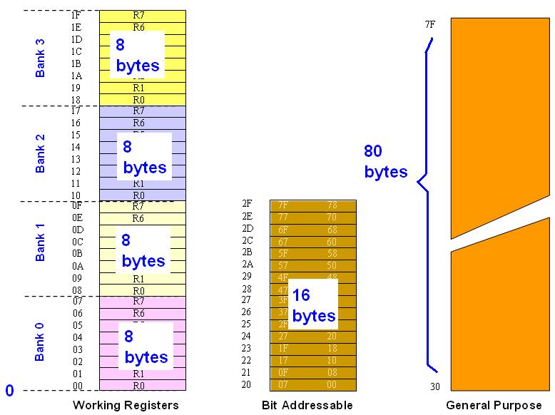
![PUSH 6 ;SP=SP+1, [SP] = [6] ;Move data from location 6 to location pointed by SP, top of stack MOV R6, #25H ;R6=25H MOV R1, #12H ;R1=12H MOV R4, #0F3H ;R4=F3H PUSH 6 ;SP=SP+1, Push data from location](/docs-images/85/92295290/images/23-0.jpg "6 to location pointed by SP PUSH 1 ;SP=SP+1, Push data from location 1 to location pointed by SP PUSH 4 ;SP=SP+1, Push data from location 4 to location pointed by SP POP 3 ;POP data from location")
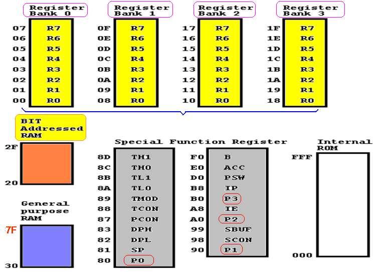
23 PUSH 6 ;SP=SP+1, [SP] = [6] ;Move data from location 6 to location pointed by SP, top of stack MOV R6, #25H ;R6=25H MOV R1, #12H ;R1=12H MOV R4, #0F3H ;R4=F3H PUSH 6 ;SP=SP+1, Push data from location 6 to location pointed by SP PUSH 1 ;SP=SP+1, Push data from location 1 to location pointed by SP PUSH 4 ;SP=SP+1, Push data from location 4 to location pointed by SP POP 3 ;POP data from location pointed by SP into location 3, SP=SP-1 POP 5 ;POP data from location pointed by SP into location 5, SP=SP-1 POP 2 ;POP data from location pointed by SP into location 2, SP=SP-1 MOV A, #55H ;A = 55H= b BACK: MOV P0, A ;Move A to Port 0 ACALL DELAY ;Call Delay routine (sub-program) CPL A ;Complement A, b b ;Complement 55H AAH ;Complement AAH 55H SJMP BACK ;Jump to label BACK Port 0, bit 0-23-
24 MOV A, #0FFH ;Write 1 to Port 0 ;F F H = b MOV P0, A ;Set Port 0 as input BACK: MOV A, P0 ;Read Port 0, move data to A MOV P1, A ;Move data from A to Port 1 SJMP BACK ;Jump to label BACK MOV A, #0FFH ;Set Port 1 MOV P1, A ;as input MOV A, P1 ;Read P1, A = P1 MOV R7, A ;R7 = A = P1 ACALL DELAY ;Call Delay MOV A, P1 ;A=P1 MOV R6, A ;R6 = A = P1 ACALL DELAY ;Call Delay MOV A, P1 ;A = P1 MOV R5, A ;R5 = A = P1 MOV A, #55H ;A= BACK: MOV P1, A ;P1 = A ACALL DELAY ;Delay CPL A ;Complement A SJMP BACK ;Jump Back MOV A, #0FFH ;Set Port 2 MOV P2, A ;as Input Port BACK: MOV A, P2 ;Read Port 2, A=P2 MOV P1, A ;Move P2 data to P1, P1=A SJMP BACK ;Jump Back Port Main Other Functions Port 0 I/O Address or Data (External) Port 1 I/O NIL Port 2 I/O Address (External) Port 3 I/O Special Functions RxD Receive (Com port) TxD Transmit (Com port) INT0 Interrupt 0 INT1 Interrupt 1 T0 Timer 0 T1 Timer 1 WR Write (external memory) RD Read (external memory) Exclusive OR OR -24-
25 X Y XOR X Y OR MOV P1, #55H ;P1 = AGAIN: XRL P1, #0FFH ;XRL : exclusive OR ; XOR Result = ; XOR Result = ACALL DELAY SJMP AGAIN BACK: CPL P1.2 ;Complement Port 1 Bit 2 ACALL DELAY SJMP BACK SETB P1.2 ;Set Port 1 Bit 2 to 1 MOV A, #45H ;A = 45H AGAIN: JNB P1.2, AGAIN ;JNB Jump, if bit equal to 0 ;If Bit 2 of Port 1 is 0 (NOT BIT), jump back to again ;Wait if Bit 2 of Port 1 is 0 MOV P0,A ;If P1.2 is 1, P0 = A=45H SETB P2.3 ;Set bit 3 of port 2 CLR P2.3 ;Clear bit 3 of Port 2-25-

26 MOV 81h, #30h ; Copy the immediate data 30h to SP -26-
27 MOV R0, #0ACh ; Copy the immediate data ACh to R0 ; (i.e. 00h) PUSH 00h ; SP=31h, address 31h contains the ; number Ach ;SP = SP + 1, [00] [SP], ;push data at location 00 to stack location pointed by SP PUSH 00h ; SP=32h, address 32h contains the ; number ACh POP 01h ; SP=31h, address R1 (i.e. 01h) ; contains the number ACh ;POP data from stack location pointed by SP to ;memory location 01, then SP=SP-1 POP 80h ; SP=30h, port 0 latch (i.e. 80h) ; contains the number Ach ;POP data from stack location pointed by SP to ;memory location 80, then SP=SP-1 ADDITION SUBTRACTION
![R7 7D 40h EB 41h + C5 42h A MOV A, 40h ; set A = RAM location 40h MOV R7, #0 ; set R7 = 0, set high byte of sum=0 ADD A, 41h ; add A with RAM location 41h ;A=A+[41h] JNC NEXT ; if CY = 0 don t](/docs-images/85/92295290/images/28-0.jpg "accumulate carry ;Jump to NEXT if NO CARRY INC R7 ; keep track of carry, R7=R7+1, Increment NEXT: ADD A, 42h ; add A with RAM location 42h ;A=A+[42h] JNC NEXT1 ; if CY = 0 don t accumulate carry INC")
28 R7 7D 40h EB 41h + C5 42h A MOV A, 40h ; set A = RAM location 40h MOV R7, #0 ; set R7 = 0, set high byte of sum=0 ADD A, 41h ; add A with RAM location 41h ;A=A+[41h] JNC NEXT ; if CY = 0 don t accumulate carry ;Jump to NEXT if NO CARRY INC R7 ; keep track of carry, R7=R7+1, Increment NEXT: ADD A, 42h ; add A with RAM location 42h ;A=A+[42h] JNC NEXT1 ; if CY = 0 don t accumulate carry INC R7 ; keep track of carry NEXT1: END 3C E7 + 3B ADDC + 8D ADD High Byte R7 Low Byte R6 CLR C ; make C=0, Clear CARRY MOV A, #0E7h ; load the low byte now A=E7h ;0E7 = Hex No. (not variable / label name) ADD A, #8Dh ; add the low byte now A=74h and C=1, A=A+ constant 8Dh MOV R6, A ; save the low byte of the sum in R6 MOV A, #3Ch ; load the high byte ADDC A, #3Bh ; add with the carry ; 3B + 3C + 1 = 78 (all in hex) MOV R7, A ; save the high byte of the sum -28-
29 A B A XOR B If you perform the following operation: A XOR #FF, if bit = 0 1, bit = 1 0 A7 A6 A5 A4 A3 A2 A1 A
 BCD data 1+BCD data 2 => Binary Addition =>Result IS NOT in BCD form, Convert the result into BCD (Decimal Adjust)")
30 Lecture 5 MOV A, #47h ; A=47h first BCD operand MOV B, #25h ; B=25h second BCD operand Decimal Addition 47 decimal + 25 decimal = 72 ADD A, B ; hex (binary) addition (A=6Ch) Binary Addition: 47h + 25h=6Ch Convert 6Ch to corresponding BCD DA A ; adjust for BCD addition (A=72h) BCD data 1+BCD data 2 => Binary Addition =>Result IS NOT in BCD form, Convert the result into BCD (Decimal Adjust) Remarks: 6Ch, C = 12 is not a BCD digit C / 10 decimal (1) => Remainder -> Lower Nipple -> Upper Nipple 6 + Quotient from (1) If we interpret 72h as a binary number then 72h 6Ch = 6 => Add 6 after binary addition -30-
 addition (A=6Ch) DA A ;adjust for BCD addition (A=72h) X(BCD) + Y(BCD) BCD Result!")
31 Lecture 6 3C E7 + 3B 8D Y X DA A The action is to decimal adjust the register A Used after the addition of two BCD numbers Example 6.4 : MOV A, #47h ; A=47h first BCD operand MOV B, #25h ; B=25h second BCD operand ADD A, B ; hex (binary) addition (A=6Ch) DA A ;adjust for BCD addition (A=72h) X(BCD) + Y(BCD) BCD Result! (but a Binary result) (Binary Addition) If we ADD 6 to the above result, the final result will be a correct BCD number MUL AB Uses registers A and B as both source and destination registers Numbers in A and B are multiplied, then put the lower-order byte of the product in A and the high-order byte in B The OV flag is set to 1 if the product > FFh Note that the C flag is 0 at all times -31-
32 A7 A6 A5 A4 A3 A2 A1 A0 X B7 B6 B5 B4 B3 B2 B1 B0 (8 bits number) x (8 bits number) = result (with 16 bits) A x B = Result B A High byte Low byte DIV AB The number in A is divided by B. The quotient is put in A and the remainder (if any) is put in B A B = Quotient & Remainder A B Format Addressing mode # Constant Immediate Register Name Register R?, A, B Hexadecimal Direct No. without only Register Address in and + A+DPTR=Address Jump Relative Instruction ACALL, Absolute AJUMP LCALL Long LJUMP -32-
33 Lecture 7 ORG 800H DELAY: MOV R1, #200 1 { 1+ LOOP: MOV R2,#255 1 [ 1+ HERE: DJNZ R2, HERE 2 (2)x255+ DJNZ R1, LOOP 2 2 ]x200+ RET 2 2 } END {1+[1+(2x255)+2]x200+2} Cycle Calculation DELAY: MOV R2, #200 1 {1+ HERE1: MOV R3,#250 1 [ 1 + HERE2: DJNZ R3, HERE2 2 (2)x250 + DJNZ R2, HERE1 2 2 ]x200+ RET 2 2} END = [1 + (2) x ] x = RL A
34 VAR1 EQU 1 VAR2 EQU 2 MOV R1,#6 MOV R2,#8 MOV A,VAR1 ; get VAR1 to A IFTEST: CJNE A, #5, NOT_EQ1 ; if VAR1 = 5 skip the THEN part SJMP ELSE1 ; and do ELSE part NOT_EQ1: JC ELSE1 ; if VAR1 < 5 do ELSE part too MOV A,VAR2 ; now the && part of conditional, CJNE A, #10, NOT_EQ2 ; i.e. checking VAR2 JMP ELSE1 ; if equal do ELSE part NOT_EQ2: JNC ELSE1 ; if VAR2 > 10 do ELSE part THEN: INC R7 ; finally, if (VAR1 > 0) && (VAR2 < 10) SJMP CONTINUE ELSE1: DEC R7 ; perform ELSE part i.e. SUM = SUM V 1 CONTINUE: SJMP CONTINUE END MAX EQU 1 NEW EQU 2 MOV R1,#20 MOV R2,#30 MOV A, NEW ; get NEW IFTEST: CJNE A, MAX, NOT_EQ ; condition testing SJMP CONTINUE ;If EQUAL EXIT NOT_EQ: JC CONTINUE ; jump if NEW < MAX THEN: MOV MAX, A ; do then part since NEW > MAX CONTINUE: SJMP CONTINUE ;; the rest of the program END SUM EQU 0 COUNT EQU 1 ORG 0H MOV SUM,#0 ; initialize SUM MOV A,SUM ; use A as the temporary storage ; for SUM MOV COUNT,#10 ; initialize COUNT FOR_LP: ADD A, COUNT ;A=A+Count DJNZ COUNT,FOR_LP ;COUNT=COUNT-1 END_FOR: SJMP CONTINUE CONTINUE: SJMP CONTINUE ;; the rest of the program END -34-
35 Lecture 8 1. Timer Counter Counter Value increment at each cycle 0000H FFFFH (16 bits), TH, TL 2. Timer Control Timer ON/OFF, TCON 3. Timer Mode Mode settings of timer, TMOD GATE=ON, Timer 0 Enable when TR0=High AND INT0=High GATE=OFF, Timer 0 Enable when TR0=High GATE Use External INT0 signal as ON/OFF control? C/T Timer or Counter? M1,M0 Mode Bit -35-
36 INTERRUPT AND TIMER Example 8.7 : (a) Program the IP register to assign the highest priority to INT1, (b) Discuss what happens if INT0, INT1 and TF0 are activated at the same time. (Ans: Same as the priority after RESET) Original INT0 TF0 INT1 TF1 RI+TI INT0 > TF0 > INT1 > TF1 > RI+TI After INT1 INT0 TF0 TF1 RI+TI INT1 > INT0 > TF0 > TF1 > RI+TI Example 8.8 : The IP register is set by the instruction MOV IP, # B after reset. Discuss the sequence in which the interrupts are serviced. MOV IP, # B instruction sets INT1 & TF1 to a higher priority level compared with the rest of the interrupts Original INT0 TF0 INT1 TF1 RI+TI INT0 > TF0 > INT1 > TF1 > RI+TI After INT1 TF1 INT0 TF0 RI+TI INT1 > TF1 > INT0 > TF0 > Serial -36-

37 ORG 0000H START: MOV R0, #OK DATA+1 ;R0 = No. of byte in table MOV DPTR, #DATA ;DPTR = table start address MOV R1, #00H ;R1 = Index to row of the table LOOP: MOV A, R1 MOVC ;Move [R1+DPTR] to A MOV P1, A ACALL DELAY INC R1 ;Move to next row, R1=R1+1 DJNZ R0, LOOP ;No. of bytes remain=0? AJMP START ; DELAY: MOV R5, #2 DL1: MOV R6, #250 DL2: MOV R7, #200 DL3: DJNZ R7, DL3 DJNZ R6, DL2 DJNZ R5, DL1 ; DATA: OK: END RET DB B DB B DB B DB B DB B DB B DB B DB B DB B DB B DB B DB B DB B DB B DB B DB B DB B DB B DB B DB B -37-
38 ORG 0000H MOV R1, # B ; LED ON/OFF Patterns MOV R2, # B MOV R3, # B MOV R4, # B TEST: ORL P3, #0FFH ; Set all bits in P3 to 1, input port JNB P3.7, CASE1 ; Jump Not bit, if P3.7 is low, jump to CASE1 JNB P3.6, CASE2 JNB P3.5, CASE3 JNB P3.4, CASE4 AJMP TEST CASE1: MOV A, R1 ;A= MOV P1, A ACALL DELAY XRL A, # B ;A= MOV P1, A AJMP TEST CASE2 MOV A, R2 ;A= MOV P1, A ACALL DELAY XRL A, # B ;A= Turn OFF led MOV P1, A AJMP TEST CASE3 MOV A, R3 ;A= MOV P1, A ACALL DELAY XRL A, # B ;A= MOV P1, A AJMP TEST CASE4 MOV A, R4 ; A= MOV P1, A ACALL DELAY XRL A, # B ;A= MOV P1, A AJMP TEST DELAY:.. END -38-
39 ORG 0000H MOV R3, #00H ;R3 Data to be displayed LOOP: MOV DPTR, #TABLE ;DPTR = Table Start Address MOV A, R3 ; MOVC ;Look up [DPTR+R3] entry at data table ; Display numbers on 7-segment display MOV P1, A ;Move ON/OFF pattern to Port 1 ACALL DELAY ; Increase R3 by 1 and loop back MOV A, R3 ADD A, #1 ;R3 = R3 + 1 DA A ;Decimal Adjust ;A= = 10 decimal after DA ANL A, #0FH ;A=???????? AND ???? ;A reset to H after ANL A,#0FH MOV R3, A ;Version 2 INC R3 CJNE R3,#10,CONT1 MOV R3,#0H CONT1: AJMP LOOP ; DELAY:.. TABLE: DB B ; 0 ;7-Segment LED Patterns DB B ; 1 DB B ; 2 DB B ; 3 DB B ; 4 DB B ; 5 DB B ; 6 DB B ; 7 DB B ; 8 DB B ; 9 ; END -39-
40 Lecture 9 CS (Chip Select) Active low input used to activate the ADC0804 chip. [CS=LOW, turn ON ADC0804] RD (data enable) Active low input used to get converted data out of the ADC0804 chip. When CS = 0, if a high-tolow pulse is applied to the RD pin, the 8-bit digital output shows up at the D0-D7 data pins. [CS=0, HIGH-TO-LOW pulse to RD, Read Data at D0-D7] WR (start conversion) [CS=0, LOW-TO-HIGH pulse to WR (Write), ADC start converting data] Active low input used to inform the ADC0804 to start the conversion process. If CS = 0 when WR makes a low-to-high transition, the ADC0804 starts converting the analog input value of Vin to an 8-bit digital number. When the data conversion is complete, the INTR pin is forced low by the ADC0804. (Conversion completed=> INTR=0) CLK IN and CLK R Connect to external capacitor and resistor for self-clocking, f = 1/(1.1RC). The clock affect the conversion time and this time cannot be faster than 110µs. INTR (end of conversion) This is an active low output pin. When the conversion is finished, it goes low to signal the CPU that the converted data is ready to be picked up. After INTR goes low, we make CS = 0 and send a high-to-low pulse to the RD pin to get the data out of the ADC0804 chip. Vin (+) and Vin ( ) These are the differential analog inputs where Vin = Vin (+) Vin ( ). Often the Vin ( ) pin is connected to ground and the Vin (+) pin is used as the analog input to be converted to digital. D 7 D6 D5 D 4 D3 D 2 D1 D0 I out = I ref D7 64 D6 32 D5 16 D4 8 D3 4 D2 2D1 D0 I out = I ref Iout = Iref (128 D D D D4 + 8 D3 + 4 D2 + D0) / 256 I out = I ref (2 7 D D D D D D D D 0 ) / 256 I out = I ref (Convert D0-D7 from binary to Decimal)/ is full scale Iout is proportional to the decimal value of D0-D7 D 7 D6 D5 D 4 D3 D 2 D1 D0 I out = I ref I out = I ref (2 7 D D D D D D D D 0 ) / 256 I out = I ref (Convert D0-D7 from binary to Decimal)/256 I out = (D0-D7 in decimal form) / 256 x I ref 256 is full scale, I out is proportional to the decimal value of D0-D7-40-
41 Lecture
42 Step # Winding A Winding B Winding A Winding B Step # Winding A Winding B Winding A Winding B Step # Winding Winding Winding Winding Winding Winding Winding Winding A B A B A B A B Step # Winding Winding Winding Winding Winding Winding Winding Winding A B A B A B A B
43 -43-
LABORATORY MANUAL MICROPROCESSOR AND MICROCONTROLLER
 LABORATORY MANUAL S u b j e c t : MICROPROCESSOR AND MICROCONTROLLER TE (E lectr onics) ( S e m V ) 1 I n d e x Serial No T i tl e P a g e N o M i c r o p r o c e s s o r 8 0 8 5 1 8 Bit Addition by Direct
System Data Bus (8-bit) Data Buffer. Internal Data Bus (8-bit) 8-bit register (R) 3-bit address 16-bit register pair (P) 2-bit address
 Data Buffer. Internal Data Bus (8-bit) 8-bit register (R) 3-bit address 16-bit register pair (P) 2-bit address") Intel 8080 CPU block diagram 8 System Data Bus (8-bit) Data Buffer Registry Array B 8 C Internal Data Bus (8-bit) F D E H L ALU SP A PC Address Buffer 16 System Address Bus (16-bit) Internal register addressing:
Intel 8080 CPU block diagram 8 System Data Bus (8-bit) Data Buffer Registry Array B 8 C Internal Data Bus (8-bit) F D E H L ALU SP A PC Address Buffer 16 System Address Bus (16-bit) Internal register addressing:
LABORATORY MANUAL MICROPROCESSORS AND MICROCONTROLLERS. S.E (I.T) ( S e m. IV)
 ( S e m. IV)") LABORATORY MANUAL MICROPROCESSORS AND MICROCONTROLLERS S.E (I.T) ( S e m. IV) 1 I n d e x Serial No. T i tl e P a g e N o. 1 8 bit addition with carry 3 2 16 bit addition with carry 5 3 8 bit multiplication
LABORATORY MANUAL MICROPROCESSORS AND MICROCONTROLLERS S.E (I.T) ( S e m. IV) 1 I n d e x Serial No. T i tl e P a g e N o. 1 8 bit addition with carry 3 2 16 bit addition with carry 5 3 8 bit multiplication
Menu. Review of Number Systems EEL3701 EEL3701. Math. Review of number systems >Binary math >Signed number systems
 Menu Review of number systems >Binary math >Signed number systems Look into my... 1 Our decimal (base 10 or radix 10) number system is positional. Ex: 9437 10 = 9x10 3 + 4x10 2 + 3x10 1 + 7x10 0 We have
Fundamentals of Digital Design
 Fundamentals of Digital Design Digital Radiation Measurement and Spectroscopy NE/RHP 537 1 Binary Number System The binary numeral system, or base-2 number system, is a numeral system that represents numeric
UNIVERSITI TENAGA NASIONAL. College of Information Technology
 UNIVERSITI TENAGA NASIONAL College of Information Technology BACHELOR OF COMPUTER SCIENCE (HONS.) FINAL EXAMINATION SEMESTER 2 2012/2013 DIGITAL SYSTEMS DESIGN (CSNB163) January 2013 Time allowed: 3 hours
3. Complete the following table of equivalent values. Use binary numbers with a sign bit and 7 bits for the value
 EGC22 Digital Logic Fundamental Additional Practice Problems. Complete the following table of equivalent values. Binary. Octal 35.77 33.23.875 29.99 27 9 64 Hexadecimal B.3 D.FD B.4C 2. Calculate the following
Numbering Systems. Contents: Binary & Decimal. Converting From: B D, D B. Arithmetic operation on Binary.
 Numbering Systems Contents: Binary & Decimal. Converting From: B D, D B. Arithmetic operation on Binary. Addition & Subtraction using Octal & Hexadecimal 2 s Complement, Subtraction Using 2 s Complement.
Design of Sequential Circuits
 Design of Sequential Circuits Seven Steps: Construct a state diagram (showing contents of flip flop and inputs with next state) Assign letter variables to each flip flop and each input and output variable
ALU (3) - Division Algorithms
 - Division Algorithms") HUMBOLDT-UNIVERSITÄT ZU BERLIN INSTITUT FÜR INFORMATIK Lecture 12 ALU (3) - Division Algorithms Sommersemester 2002 Leitung: Prof. Dr. Miroslaw Malek www.informatik.hu-berlin.de/rok/ca CA - XII - ALU(3)
HUMBOLDT-UNIVERSITÄT ZU BERLIN INSTITUT FÜR INFORMATIK Lecture 12 ALU (3) - Division Algorithms Sommersemester 2002 Leitung: Prof. Dr. Miroslaw Malek www.informatik.hu-berlin.de/rok/ca CA - XII - ALU(3)
Chapter 7. Sequential Circuits Registers, Counters, RAM
 Chapter 7. Sequential Circuits Registers, Counters, RAM Register - a group of binary storage elements suitable for holding binary info A group of FFs constitutes a register Commonly used as temporary storage
PAST EXAM PAPER & MEMO N3 ABOUT THE QUESTION PAPERS:
 EKURHULENI TECH COLLEGE. No. 3 Mogale Square, Krugersdorp. Website: www. ekurhulenitech.co.za Email: info@ekurhulenitech.co.za TEL: 011 040 7343 CELL: 073 770 3028/060 715 4529 PAST EXAM PAPER & MEMO N3
MAHARASHTRA STATE BOARD OF TECHNICAL EDUCATION (Autonomous) (ISO/IEC Certified) State any two Boolean laws. (Any 2 laws 1 mark each)
 (ISO/IEC Certified) State any two Boolean laws. (Any 2 laws 1 mark each)") Subject Code: 17333 Model Answer Page 1/ 27 Important Instructions to examiners: 1) The answers should be examined by key words and not as word-to-word as given in the model answer scheme. 2) The model
Subject Code: 17333 Model Answer Page 1/ 27 Important Instructions to examiners: 1) The answers should be examined by key words and not as word-to-word as given in the model answer scheme. 2) The model
PART-A. 2. Expand ASCII and BCD ASCII American Standard Code for Information Interchange BCD Binary Coded Decimal
 PART-A 1. What is radix? Give the radix for binary, octal, decimal and hexadecimal Radix is the total number of digits used in a particular number system Binary - 2 (0,1) Octal - 8 (0 to 7) Decimal - 10
Numbers and Arithmetic
 Numbers and Arithmetic See: P&H Chapter 2.4 2.6, 3.2, C.5 C.6 Hakim Weatherspoon CS 3410, Spring 2013 Computer Science Cornell University Big Picture: Building a Processor memory inst register file alu
Numbers and Arithmetic
 Numbers and Arithmetic See: P&H Chapter 2.4 2.6, 3.2, C.5 C.6 Hakim Weatherspoon CS 3410, Spring 2013 Computer Science Cornell University Big Picture: Building a Processor memory inst register file alu
Hakim Weatherspoon CS 3410 Computer Science Cornell University
 Hakim Weatherspoon CS 3410 Computer Science Cornell University The slides are the product of many rounds of teaching CS 3410 by Professors Weatherspoon, Bala, Bracy, and Sirer. memory inst 32 register
An Alternative Method for Resolution Improvement to Rotary Incremental Encoder
 Proceedings of the 2nd WSEAS/IASME International Conference on Educational Technologies, Bucharest, Romania, October 16-17, 2006 33 An Alternative Method for Resolution Improvement to Rotary Incremental
Please read carefully. Good luck & Go Gators!!!
 Page 1/12 Exam 1 May the Schwartz be with you! Instructions: Turn off all cell phones and other noise making devices and put away all electronics Show all work on the front of the test papers Box each
Shift Register Counters
 Shift Register Counters Shift register counter: a shift register with the serial output connected back to the serial input. They are classified as counters because they give a specified sequence of states.
CprE 281: Digital Logic
 CprE 28: Digital Logic Instructor: Alexander Stoytchev http://www.ece.iastate.edu/~alexs/classes/ Simple Processor CprE 28: Digital Logic Iowa State University, Ames, IA Copyright Alexander Stoytchev Digital
hexadecimal-to-decimal conversion
 OTHER NUMBER SYSTEMS: octal (digits 0 to 7) group three binary numbers together and represent as base 8 3564 10 = 110 111 101 100 2 = (6X8 3 ) + (7X8 2 ) + (5X8 1 ) + (4X8 0 ) = 6754 8 hexadecimal (digits
Unit II Chapter 4:- Digital Logic Contents 4.1 Introduction... 4
 Unit II Chapter 4:- Digital Logic Contents 4.1 Introduction... 4 4.1.1 Signal... 4 4.1.2 Comparison of Analog and Digital Signal... 7 4.2 Number Systems... 7 4.2.1 Decimal Number System... 7 4.2.2 Binary
WTR-S4 Module User Manual WTR-S4 MODULE
 WTR-S MODULE.PRODUCT FEATURES....FUTION DESCRIPTIONS....RELATIONSHIP OF FLASH MEMORY CAPACITY AND RECORDING DURATION....APPLICATION DIAGRAM....PACKAGE SKETCH MAP....PIN DESCRIPTIONS.... SAMPLING RATE SETTINGS....PARAMETERS...
Number Systems 1(Solutions for Vol 1_Classroom Practice Questions)
") Chapter Number Systems (Solutions for Vol _Classroom Practice Questions). ns: (d) 5 x + 44 x = x ( x + x + 5 x )+( x +4 x + 4 x ) = x + x + x x +x+5+x +4x+4 = x + x + x 5x 6 = (x6) (x+ ) = (ase cannot
Chapter Number Systems (Solutions for Vol _Classroom Practice Questions). ns: (d) 5 x + 44 x = x ( x + x + 5 x )+( x +4 x + 4 x ) = x + x + x x +x+5+x +4x+4 = x + x + x 5x 6 = (x6) (x+ ) = (ase cannot
Conversions between Decimal and Binary
 Conversions between Decimal and Binary Binary to Decimal Technique - use the definition of a number in a positional number system with base 2 - evaluate the definition formula ( the formula ) using decimal
Lecture 1. How to Boot a PC. Andrei Pitiș. October 8, Operating Systems Practical. OSP Lecture 1, Booting 1/30
 Lecture 1 How to Boot a PC Andrei Pitiș Operating Systems Practical October 8, 2014 OSP Lecture 1, Booting 1/30 Table of Contents Hardware Processor Memory I/O subsystems Boot Process Keywords Resources
CHW 261: Logic Design
 CHW 26: Logic Design Instructors: Prof. Hala Zayed Dr. Ahmed Shalaby http://www.bu.edu.eg/staff/halazayed4 http://bu.edu.eg/staff/ahmedshalaby4# Slide Digital Fundamentals Digital Concepts Slide 2 What?
Layout of 7400-series Chips Commonly Used in. CDA 3101: Introduction to Computer Hardware and Organization
 Layout of 400-series Chips Commonly Used in CDA 30: Introduction to Computer Hardware and Organization Charles N. Winton Department of Computer and Information Sciences University of North Florida 999
Lab 3 Revisited. Zener diodes IAP 2008 Lecture 4 1
 Lab 3 Revisited Zener diodes R C 6.091 IAP 2008 Lecture 4 1 Lab 3 Revisited +15 Voltage regulators 555 timers 270 1N758 0.1uf 5K pot V+ V- 2N2222 0.1uf V o. V CC V Vin s = 5 V Vc V c Vs 1 e t = RC Threshold
University of Florida EEL 3701 Fall 2014 Dr. Eric. M. Schwartz Department of Electrical & Computer Engineering Wednesday, 15 October 2014
 Page 1/12 Exam 1 May the Schwartz Instructions: be with you! Turn off all cell phones and other noise making devices and put away all electronics Show all work on the front of the test papers Box each
ECE380 Digital Logic. Positional representation
 ECE380 Digital Logic Number Representation and Arithmetic Circuits: Number Representation and Unsigned Addition Dr. D. J. Jackson Lecture 16-1 Positional representation First consider integers Begin with
S.Y. Diploma : Sem. III [DE/ED/EI/EJ/EN/ET/EV/EX/IC/IE/IS/IU/MU] Principles of Digital Techniques
![S.Y. Diploma : Sem. III [DE/ED/EI/EJ/EN/ET/EV/EX/IC/IE/IS/IU/MU] Principles of Digital Techniques](/thumbs/82/86792063.jpg "S.Y. Diploma : Sem. III [DE/ED/EI/EJ/EN/ET/EV/EX/IC/IE/IS/IU/MU] Principles of Digital Techniques") S.Y. Diploma : Sem. III [DE/ED/EI/EJ/EN/ET/EV/EX/IC/IE/IS/IU/MU] Principles of Digital Techniques Time: 3 Hrs.] Prelim Question Paper Solution [Marks : 100 Q.1(a) Attempt any SIX of the following : [12]
S.Y. Diploma : Sem. III [DE/ED/EI/EJ/EN/ET/EV/EX/IC/IE/IS/IU/MU] Principles of Digital Techniques Time: 3 Hrs.] Prelim Question Paper Solution [Marks : 100 Q.1(a) Attempt any SIX of the following : [12]
ENGIN 112 Intro to Electrical and Computer Engineering
 ENGIN 112 Intro to Electrical and Computer Engineering Lecture 3 More Number Systems Overview Hexadecimal numbers Related to binary and octal numbers Conversion between hexadecimal, octal and binary Value
MATH Dr. Halimah Alshehri Dr. Halimah Alshehri
 MATH 1101 haalshehri@ksu.edu.sa 1 Introduction To Number Systems First Section: Binary System Second Section: Octal Number System Third Section: Hexadecimal System 2 Binary System 3 Binary System The binary
Introduction EE 224: INTRODUCTION TO DIGITAL CIRCUITS & COMPUTER DESIGN. Lecture 6: Sequential Logic 3 Registers & Counters 5/9/2010
 EE 224: INTROUCTION TO IGITAL CIRCUITS & COMPUTER ESIGN Lecture 6: Sequential Logic 3 Registers & Counters 05/10/2010 Avinash Kodi, kodi@ohio.edu Introduction 2 A Flip-Flop stores one bit of information
Boolean Algebra and Digital Logic 2009, University of Colombo School of Computing
 IT 204 Section 3.0 Boolean Algebra and Digital Logic Boolean Algebra 2 Logic Equations to Truth Tables X = A. B + A. B + AB A B X 0 0 0 0 3 Sum of Products The OR operation performed on the products of
DIGITAL LOGIC CIRCUITS
 DIGITAL LOGIC CIRCUITS Digital logic circuits BINARY NUMBER SYSTEM electronic circuits that handle information encoded in binary form (deal with signals that have only two values, and ) Digital. computers,
Digital Electronic Meters
 Digital Electronic Meters EIE 240 Electrical and Electronic Measurement May 1, 2015 1 Digital Signal Binary or two stages: 0 (Low voltage 0-3 V) 1 (High voltage 4-5 V) Binary digit is called bit. Group
University of Florida EEL 3701 Summer 2015 Dr. Eric. M. Schwartz Department of Electrical & Computer Engineering Tuesday, 30 June 2015
 University of Florida EEL 3701 Summer 2015 Dr Eric M Schwartz Page 1/13 Exam 1 May the Schwartz be with you! Instructions: Turn off all cell phones and other noise making devices Show all work on the front
Digital Signal 2 N Most Significant Bit (MSB) Least. Bit (LSB)
 Least. Bit (LSB)") 1 Digital Signal Binary or two stages: 0 (Low voltage 0-3 V) 1 (High voltage 4-5 V) Binary digit is called bit. Group of bits is called word. 8-bit group is called byte. For N-bit base-2 number = 2 N levels
1 Digital Signal Binary or two stages: 0 (Low voltage 0-3 V) 1 (High voltage 4-5 V) Binary digit is called bit. Group of bits is called word. 8-bit group is called byte. For N-bit base-2 number = 2 N levels
EECS 270 Midterm Exam 2 Fall 2009
 EECS 270 Midterm Exam 2 Fall 2009 Name: unique name: UMID: Sign the honor code: I have neither given nor received aid on this exam nor observed anyone else doing so. Scores: NOTES: Problem # Points 1&2
Binary addition example worked out
 Binary addition example worked out Some terms are given here Exercise: what are these numbers equivalent to in decimal? The initial carry in is implicitly 0 1 1 1 0 (Carries) 1 0 1 1 (Augend) + 1 1 1 0
ELEN Electronique numérique
 ELEN0040 - Electronique numérique Patricia ROUSSEAUX Année académique 2014-2015 CHAPITRE 3 Combinational Logic Circuits ELEN0040 3-4 1 Combinational Functional Blocks 1.1 Rudimentary Functions 1.2 Functions
ALU A functional unit
 ALU A functional unit that performs arithmetic operations such as ADD, SUB, MPY logical operations such as AND, OR, XOR, NOT on given data types: 8-,16-,32-, or 64-bit values A n-1 A n-2... A 1 A 0 B n-1
Logic Design II (17.342) Spring Lecture Outline
 Spring Lecture Outline") Logic Design II (17.342) Spring 2012 Lecture Outline Class # 10 April 12, 2012 Dohn Bowden 1 Today s Lecture First half of the class Circuits for Arithmetic Operations Chapter 18 Should finish at least
Logic Design II (17.342) Spring 2012 Lecture Outline Class # 10 April 12, 2012 Dohn Bowden 1 Today s Lecture First half of the class Circuits for Arithmetic Operations Chapter 18 Should finish at least
CMP 334: Seventh Class
 CMP 334: Seventh Class Performance HW 5 solution Averages and weighted averages (review) Amdahl's law Ripple-carry adder circuits Binary addition Half-adder circuits Full-adder circuits Subtraction, negative
Schedule. ECEN 301 Discussion #25 Final Review 1. Date Day Class No. 1 Dec Mon 25 Final Review. Title Chapters HW Due date. Lab Due date.
 Schedule Date Day Class No. Dec Mon 25 Final Review 2 Dec Tue 3 Dec Wed 26 Final Review Title Chapters HW Due date Lab Due date LAB 8 Exam 4 Dec Thu 5 Dec Fri Recitation HW 6 Dec Sat 7 Dec Sun 8 Dec Mon
S.Y. Diploma : Sem. III [CO/CM/IF/CD/CW] Digital Techniques
![S.Y. Diploma : Sem. III [CO/CM/IF/CD/CW] Digital Techniques](/thumbs/90/103932933.jpg "S.Y. Diploma : Sem. III [CO/CM/IF/CD/CW] Digital Techniques") S.Y. Diploma : Sem. III [CO/CM/IF/CD/CW] Digital Techniques Time: 3 Hrs.] Prelim Question Paper Solution [Marks : 100 Q.1(a) Attempt any SIX of the following : [12] Q.1(a) (i) Derive AND gate and OR gate
S.Y. Diploma : Sem. III [CO/CM/IF/CD/CW] Digital Techniques Time: 3 Hrs.] Prelim Question Paper Solution [Marks : 100 Q.1(a) Attempt any SIX of the following : [12] Q.1(a) (i) Derive AND gate and OR gate
Digital Circuits. 1. Inputs & Outputs are quantized at two levels. 2. Binary arithmetic, only digits are 0 & 1. Position indicates power of 2.
 Digital Circuits 1. Inputs & Outputs are quantized at two levels. 2. inary arithmetic, only digits are 0 & 1. Position indicates power of 2. 11001 = 2 4 + 2 3 + 0 + 0 +2 0 16 + 8 + 0 + 0 + 1 = 25 Digital
Adders, subtractors comparators, multipliers and other ALU elements
 CSE4: Components and Design Techniques for Digital Systems Adders, subtractors comparators, multipliers and other ALU elements Adders 2 Circuit Delay Transistors have instrinsic resistance and capacitance
MODEL ANSWER SUMMER 17 EXAMINATION Subject Title: Principles of Digital Techniques
 MODEL ANSWER SUMMER 17 EXAMINATION Subject Title: Principles of Digital Techniques Subject Code: Important Instructions to examiners: 1) The answers should be examined by key words and not as word-to-word
SUMMER 18 EXAMINATION Subject Name: Principles of Digital Techniques Model Answer Subject Code:
 Important Instructions to examiners: 1) The answers should be examined by key words and not as word-to-word as given in the model answer scheme. 2) The model answer and the answer written by candidate
Sample Test Paper - I
 Scheme G Sample Test Paper - I Course Name : Computer Engineering Group Marks : 25 Hours: 1 Hrs. Q.1) Attempt any THREE: 09 Marks a) Define i) Propagation delay ii) Fan-in iii) Fan-out b) Convert the following:
SIR C.R.REDDY COLLEGE OF ENGINEERING ELURU DIGITAL INTEGRATED CIRCUITS (DIC) LABORATORY MANUAL III / IV B.E. (ECE) : I - SEMESTER
 LABORATORY MANUAL III / IV B.E. (ECE) : I - SEMESTER") SIR C.R.REDDY COLLEGE OF ENGINEERING ELURU 534 007 DIGITAL INTEGRATED CIRCUITS (DIC) LABORATORY MANUAL III / IV B.E. (ECE) : I - SEMESTER DEPARTMENT OF ELECTRONICS AND COMMUNICATION ENGINEERING DIGITAL
SIR C.R.REDDY COLLEGE OF ENGINEERING ELURU 534 007 DIGITAL INTEGRATED CIRCUITS (DIC) LABORATORY MANUAL III / IV B.E. (ECE) : I - SEMESTER DEPARTMENT OF ELECTRONICS AND COMMUNICATION ENGINEERING DIGITAL
MAHARASHTRA STATE BOARD OF TECHNICAL EDUCATION (Autonomous) (ISO/IEC Certified)
 (ISO/IEC Certified)") WINTER 17 EXAMINATION Subject Name: Digital Techniques Model Answer Subject Code: 17333 Important Instructions to examiners: 1) The answers should be examined by key words and not as word-to-word as given
WINTER 17 EXAMINATION Subject Name: Digital Techniques Model Answer Subject Code: 17333 Important Instructions to examiners: 1) The answers should be examined by key words and not as word-to-word as given
on candidate s understanding. 7) For programming language papers, credit may be given to any other program based on equivalent concept.
 For programming language papers, credit may be given to any other program based on equivalent concept.") WINTER 17 EXAMINATION Subject Name: Digital Techniques Model Answer Subject Code: 17333 Important Instructions to examiners: 1) The answers should be examined by key words and not as word-to-word as given
WINTER 17 EXAMINATION Subject Name: Digital Techniques Model Answer Subject Code: 17333 Important Instructions to examiners: 1) The answers should be examined by key words and not as word-to-word as given
Automata Theory CS S-12 Turing Machine Modifications
 Automata Theory CS411-2015S-12 Turing Machine Modifications David Galles Department of Computer Science University of San Francisco 12-0: Extending Turing Machines When we added a stack to NFA to get a
COE 328 Final Exam 2008
 COE 328 Final Exam 2008 1. Design a comparator that compares a 4 bit number A to a 4 bit number B and gives an Output F=1 if A is not equal B. You must use 2 input LUTs only. 2. Given the following logic
CMSC 313 Lecture 25 Registers Memory Organization DRAM
 CMSC 33 Lecture 25 Registers Memory Organization DRAM UMBC, CMSC33, Richard Chang A-75 Four-Bit Register Appendix A: Digital Logic Makes use of tri-state buffers so that multiple registers
GATE SOLVED PAPER - EC
 2013 ONE MARK Q. 1 A bulb in a staircase has two switches, one switch being at the ground floor and the other one at the first floor. The bulb can be turned ON and also can be turned OFF by any one of
14:332:231 DIGITAL LOGIC DESIGN. Why Binary Number System?
 :33:3 DIGITAL LOGIC DESIGN Ivan Marsic, Rutgers University Electrical & Computer Engineering Fall 3 Lecture #: Binary Number System Complement Number Representation X Y Why Binary Number System? Because
ECE 2300 Digital Logic & Computer Organization
 ECE 23 Digital Logic & Computer Organization Spring 28 Combinational Building Blocks Lecture 5: Announcements Lab 2 prelab due tomorrow HW due Friday HW 2 to be posted on Thursday Lecture 4 to be replayed
Basic Computer Organization and Design Part 3/3
 Basic Computer Organization and Design Part 3/3 Adapted by Dr. Adel Ammar Computer Organization Interrupt Initiated Input/Output Open communication only when some data has to be passed --> interrupt. The
HN58C66 Series word 8-bit CMOS Electrically Erasable and Programmable CMOS ROM. ADE F (Z) Rev. 6.0 Apr. 12, Description.
 Rev. 6.0 Apr. 12, Description.") 8192-word 8-bit CMOS Electrically Erasable and Programmable CMOS ROM ADE-203-375F (Z) Rev. 6.0 Apr. 12, 1995 Description The Hitachi HN58C66 is a electrically erasable and programmable ROM organized as
8192-word 8-bit CMOS Electrically Erasable and Programmable CMOS ROM ADE-203-375F (Z) Rev. 6.0 Apr. 12, 1995 Description The Hitachi HN58C66 is a electrically erasable and programmable ROM organized as
Four Important Number Systems
 Four Important Number Systems System Why? Remarks Decimal Base 10: (10 fingers) Most used system Binary Base 2: On/Off systems 3-4 times more digits than decimal Octal Base 8: Shorthand notation for working
CHAPTER 7. Exercises 17/ / /2 2 0
 CHAPTER 7 Exercises E7. (a) For the whole part, we have: Quotient Remainders 23/2 /2 5 5/2 2 2/2 0 /2 0 Reading the remainders in reverse order, we obtain: 23 0 = 0 2 For the fractional part we have 2
Review Problem 1. should be on. door state, false if light should be on when a door is open. v Describe when the dome/interior light of the car
 Review Problem 1 v Describe when the dome/interior light of the car should be on. v DriverDoorOpen = true if lefthand door open v PassDoorOpen = true if righthand door open v LightSwitch = true if light
Adders, subtractors comparators, multipliers and other ALU elements
 CSE4: Components and Design Techniques for Digital Systems Adders, subtractors comparators, multipliers and other ALU elements Instructor: Mohsen Imani UC San Diego Slides from: Prof.Tajana Simunic Rosing
LOGIC CIRCUITS. Basic Experiment and Design of Electronics
 Basic Experiment and Design of Electronics LOGIC CIRCUITS Ho Kyung Kim, Ph.D. hokyung@pusan.ac.kr School of Mechanical Engineering Pusan National University Outline Combinational logic circuits Output
CHAPTER 2 NUMBER SYSTEMS
 CHAPTER 2 NUMBER SYSTEMS The Decimal Number System : We begin our study of the number systems with the familiar decimal number system. The decimal system contains ten unique symbol 0, 1, 2, 3, 4, 5, 6,
Digital Electronics Circuits 2017
 JSS SCIENCE AND TECHNOLOGY UNIVERSITY Digital Electronics Circuits (EC37L) Lab in-charge: Dr. Shankraiah Course outcomes: After the completion of laboratory the student will be able to, 1. Simplify, design
SAU1A FUNDAMENTALS OF DIGITAL COMPUTERS
 SAU1A FUNDAMENTALS OF DIGITAL COMPUTERS Unit : I - V Unit : I Overview Fundamentals of Computers Characteristics of Computers Computer Language Operating Systems Generation of Computers 2 Definition of
LOGIC CIRCUITS. Basic Experiment and Design of Electronics. Ho Kyung Kim, Ph.D.
 Basic Experiment and Design of Electronics LOGIC CIRCUITS Ho Kyung Kim, Ph.D. hokyung@pusan.ac.kr School of Mechanical Engineering Pusan National University Digital IC packages TTL (transistor-transistor
Menu. Excitation Tables (Bonus Slide) EEL3701 EEL3701. Registers, RALU, Asynch, Synch
 EEL3701 EEL3701. Registers, RALU, Asynch, Synch") Menu Registers >Storage Registers >Shift Registers More LSI Components >Arithmetic-Logic Units (ALUs) > Carry-Look-Ahead Circuitry (skip this) Asynchronous versus Synchronous Look into my... 1 Excitation
Menu Registers >Storage Registers >Shift Registers More LSI Components >Arithmetic-Logic Units (ALUs) > Carry-Look-Ahead Circuitry (skip this) Asynchronous versus Synchronous Look into my... 1 Excitation
A crash course in Digital Logic
 crash course in Digital Logic Computer rchitecture 1DT016 distance Fall 2017 http://xyx.se/1dt016/index.php Per Foyer Mail: per.foyer@it.uu.se Per.Foyer@it.uu.se 2017 1 We start from here Gates Flip-flops
Binary addition (1-bit) P Q Y = P + Q Comments Carry = Carry = Carry = Carry = 1 P Q
 P Q Y = P + Q Comments Carry = Carry = Carry = Carry = 1 P Q") Digital Arithmetic In Chapter 2, we have discussed number systems such as binary, hexadecimal, decimal, and octal. We have also discussed sign representation techniques, for example, sign-bit representation
Digital Arithmetic In Chapter 2, we have discussed number systems such as binary, hexadecimal, decimal, and octal. We have also discussed sign representation techniques, for example, sign-bit representation
COE 202: Digital Logic Design Sequential Circuits Part 4. Dr. Ahmad Almulhem ahmadsm AT kfupm Phone: Office:
 COE 202: Digital Logic Design Sequential Circuits Part 4 Dr. Ahmad Almulhem Email: ahmadsm AT kfupm Phone: 860-7554 Office: 22-324 Objectives Registers Counters Registers 0 1 n-1 A register is a group
Save from: cs. Logic design 1 st Class أستاذ المادة: د. عماد
 Save from: www.uotiq.org/dep cs Logic design 1 st Class أستاذ المادة: د. عماد استاذة المادة: م.م ميساء Contents Lectured One: Number system operation 1- Decimal numbers. 2- Binary numbers. 3- Octal numbers.
EE260: Digital Design, Spring n Digital Computers. n Number Systems. n Representations. n Conversions. n Arithmetic Operations.
 EE 260: Introduction to Digital Design Number Systems Yao Zheng Department of Electrical Engineering University of Hawaiʻi at Mānoa Overview n Digital Computers n Number Systems n Representations n Conversions
Digital Logic Appendix A
 Digital Logic Appendix A Boolean Algebra Gates Combinatorial Circuits Sequential Circuits 1 Boolean Algebra George Boole ideas 1854 Claude Shannon, apply to circuit design, 1938 Describe digital circuitry
King Fahd University of Petroleum and Minerals College of Computer Science and Engineering Computer Engineering Department
 King Fahd University of Petroleum and Minerals College of Computer Science and Engineering Computer Engineering Department Page 1 of 13 COE 202: Digital Logic Design (3-0-3) Term 112 (Spring 2012) Final
Practice Homework Solution for Module 4
 Practice Homework Solution for Module 4 1. Tired of writing the names of those you want kicked off the island on cards, you wish to modernize the voting scheme used on Digital Survivor. Specifically, you
Review: Designing with FSM. EECS Components and Design Techniques for Digital Systems. Lec09 Counters Outline.
 Review: Designing with FSM EECS 150 - Components and Design Techniques for Digital Systems Lec09 Counters 9-28-04 David Culler Electrical Engineering and Computer Sciences University of California, Berkeley
Chapter 5. Digital Design and Computer Architecture, 2 nd Edition. David Money Harris and Sarah L. Harris. Chapter 5 <1>
 Chapter 5 Digital Design and Computer Architecture, 2 nd Edition David Money Harris and Sarah L. Harris Chapter 5 Chapter 5 :: Topics Introduction Arithmetic Circuits umber Systems Sequential Building
Department of Electrical & Electronics EE-333 DIGITAL SYSTEMS
 Department of Electrical & Electronics EE-333 DIGITAL SYSTEMS 1) Given the two binary numbers X = 1010100 and Y = 1000011, perform the subtraction (a) X -Y and (b) Y - X using 2's complements. a) X = 1010100
DE58/DC58 LOGIC DESIGN DEC 2014
 Q.2 a. In a base-5 number system, 3 digit representations is used. Find out (i) Number of distinct quantities that can be represented.(ii) Representation of highest decimal number in base-5. Since, r=5
UNIT II COMBINATIONAL CIRCUITS:
 UNIT II COMBINATIONAL CIRCUITS: INTRODUCTION: The digital system consists of two types of circuits, namely (i) (ii) Combinational circuits Sequential circuits Combinational circuit consists of logic gates
Preparation of Examination Questions and Exercises: Solutions
 Questions Preparation of Examination Questions and Exercises: Solutions. -bit Subtraction: DIF = B - BI B BI BO DIF 2 DIF: B BI 4 6 BI 5 BO: BI BI 4 5 7 3 2 6 7 3 B B B B B DIF = B BI ; B = ( B) BI ( B),
The Design Procedure. Output Equation Determination - Derive output equations from the state table
 The Design Procedure Specification Formulation - Obtain a state diagram or state table State Assignment - Assign binary codes to the states Flip-Flop Input Equation Determination - Select flipflop types
ECE20B Final Exam, 200 Point Exam Closed Book, Closed Notes, Calculators Not Allowed June 12th, Name
 C20B Final xam, 200 Point xam Closed Book, Closed Notes, Calculators Not llowed June 2th, 2003 Name Guidelines: Please remember to write your name on your bluebook, and when finished, to staple your solutions
Digital Systems Roberto Muscedere Images 2013 Pearson Education Inc. 1
 Digital Systems Digital systems have such a prominent role in everyday life The digital age The technology around us is ubiquitous, that is we don t even notice it anymore Digital systems are used in:
HN58C65 Series word 8-bit Electrically Erasable and Programmable CMOS ROM
 8192-word 8-bit Electrically Erasable and Programmable CMOS ROM ADE-203-374A (Z) Rev. 1.0 Apr. 12, 1995 Description The Hitachi HN58C65 is a electrically erasable and programmable ROM organized as 8192-word
Stop Watch (System Controller Approach)
") Stop Watch (System Controller Approach) Problem Design a stop watch that can measure times taken for two events Inputs CLK = 6 Hz RESET: Asynchronously reset everything X: comes from push button First
Stop Watch (System Controller Approach) Problem Design a stop watch that can measure times taken for two events Inputs CLK = 6 Hz RESET: Asynchronously reset everything X: comes from push button First
HN58C256 Series word 8-bit Electrically Erasable and Programmable CMOS ROM
 32768-word 8-bit Electrically Erasable and Programmable CMOS ROM ADE-203-092G (Z) Rev. 7.0 Nov. 29, 1994 Description The Hitachi HN58C256 is a electrically erasable and programmable ROM organized as 32768-word
Digital Electronics II Mike Brookes Please pick up: Notes from the front desk
 NOTATION.PPT(10/8/2010) 1.1 Digital Electronics II Mike Brookes Please pick up: Notes from the front desk 1. What does Digital mean? 2. Where is it used? 3. Why is it used? 4. What are the important features
Digital Circuits ECS 371
 Digital Circuits ECS 371 Dr. Prapun Suksompong prapun@siit.tu.ac.th Lecture 18 Office Hours: BKD 3601-7 Monday 9:00-10:30, 1:30-3:30 Tuesday 10:30-11:30 1 Announcement Reading Assignment: Chapter 7: 7-1,
Boolean Algebra. Digital Logic Appendix A. Postulates, Identities in Boolean Algebra How can I manipulate expressions?
 Digital Logic Appendix A Gates Combinatorial Circuits Sequential Circuits Other operations NAND A NAND B = NOT ( A ANDB) = AB NOR A NOR B = NOT ( A ORB) = A + B Truth tables What is the result of the operation
,- # (%& ( = 0,% % <,( #, $ <<,( > 0,% #% ( - + % ,'3-% & '% #% <,( #, $ <<,(,9 (% +('$ %(- $'$ & " ( (- +' $%(& 2,#. = '%% ($ (- +' $ '%("
 FEATURES!" #$$ % %&' % '( $ %( )$*++$ '(% $ *++$ %(%,- *(% (./ *( #'% # *( 0% ( *( % #$$ *( '( + 2' %( $ '( 2! '3 ((&!( *( 4 '3.%" / '3 3.% 7" 28" 9' 9,*: $ 9,*: $% (+'( / *(.( # ( 2(- %3 # $((% # ;' '3$-,(
Ch 9. Sequential Logic Technologies. IX - Sequential Logic Technology Contemporary Logic Design 1
 Ch 9. Sequential Logic Technologies Technology Contemporary Logic Design Overview Basic Sequential Logic Components FSM Design with Counters FSM Design with Programmable Logic FSM Design with More Sophisticated