Design of Combinational Logic
|
|
|
- Clyde Henry
- 5 years ago
- Views:
Transcription

1 Pune Vidyarthi Griha s COLLEGE OF ENGINEERING, NASHIK 3. Design of Combinational Logic By Prof. Anand N. Gharu (Assistant Professor) PVGCOE Computer Dept.. 30 th June 2017
2 CONTENTS :- 1. Code Converter - BCD - EXCESS-3 - Gray Code - Binary Code 2. Half Adder, Full Adder, Half Substractor, Full Substractor 3. Binary Adder (IC 7483) 4. BCD Adder 5. Look Ahead Carry Generator 6. Multiplexers (MUX) (IC 74151, 74153) 7. Demultiplexers (DEMUX) (IC 74138, 74154) 8. Comparators 9. Parity Generator and Checker
3 INTRODUCTION OF COMBINATIONAL CIRCUITS Logic circuits for digital systems may be combinational or sequential. A combinational circuit consists of input variables, logic gates, and output variables 1. Combination Circuits : - The output of combinational circuit at any instant, depends only on the levels present at input terminals. - It does not use any memory - it can have number inputs and outputs. Example: 1. Adder, Substractor 2. Comparator 3. Code Converters 4. Encoders, Decoders 5. Multiplexers and Demutiplexers
4 Code Converters Code converters take an input code, translate to its equivalent output code. Input code Code converter Output code Example: BCD to Excess-3 Code Converter. Input: BCD digit Output: Excess-3 digit 4
5 Binary Codes An n-bit binary code is a group of n bits that assume up to 2 n distinct combinations of 1s and 0s, with each combination representing one element of the set being coded For the 10 digits need a 4 bit code. One code is called Binary Coded Decimal (BCD) 5
6 Binary Coded Decimal Decimal Digit BCD Note: 1010, 1011, 1100, 1101, 1110, and 1111 are INVALID CODE! Let s crack these ex1: dec-to-bcd ex2: BCD-to-dec (a) 35 (b) 98 (c) 170 (d) 2469 (a) (b) (c)
7 Excess-3 BCD Code Decimal digits Excess-3 BCD code
8 Excess-3 Code (XS-3) Decimal No. BCD Code Excess-3 Code= BCD + Excess /29/2017 Amit Nevase 8
9 Excess-3 Code (XS-3) Example 1: Obtain Xs-3 Code for 428 Decimal 8/29/2017 Amit Nevase 9
10 Excess-3 Code (XS-3) Example 1: Obtain Xs-3 Code for 428 Decimal /29/2017 Amit Nevase 10
11 Exercise Convert following Decimal Numbers into Excess- 3 Code 1. (40) (88) (64) (23) 10 8/29/2017 Amit Nevase 11
 x = S")
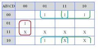
12 BCD-to-Excess-3 Code Converter Truth table: BCD Excess-3 A B C D W X Y Z X X X X X X X X X X X X X X X X X X X X X X X X W = S m(5,6,7,8,9) x = S m(1,2,3,4,9) y = S m(0,3,4,7,8) z = S m(0,2,4,6,8) 12
13 W = Sm(5,6,7,8,9)+ Sd(10,11,12,13,14,15) = a+bc+bd = a+b(c+d) AB CD 00 x AB 00 CD x 1 x x x x y = Sm(0,3,4,7,8)+ Sd(10,11,12,13,14,15) 0 1 = c d +cd x 1 x x x x x x =Sm(1,2,3,4,9)+ Sd(10,11,12,13,14,15) bc d +b d+b c=bc d +b (c+d) AB CD Underlined 00 1 x terms are 01 1 x common 11 1 x x x x = d AB CD x z = Sm(0,2,4,6,8)+ Sd(10,11,12,13,14,15) x x x x x
14 The Excess-3 BCD system is formed by adding 0011 to each BCD value as in Table 2. For example, the decimal number 7, which is coded as 0111 in BCD, is coded as =1010 in Excess-3 BCD. Decimal Numerals Excess
15 THE BCD TO EXCESS 3 CODE CONVERTER BCD Excess-3 circuit will convert numbers from their binary representation to their excess-3 representation. Hence our truth table is as below: B3 B2 B1 B0 E3 E2 E1 E
16 E2=B2^(B1+B0)
17 E1=(B1^B0)
18 E0=B0
19 Block diagram
20 Applications Excess-3 was used on some older computers Cash registers Hand held portable electronic calculators
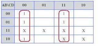
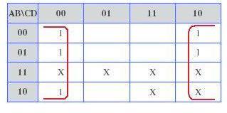
21 BCD to XS 3 code converter- Design (1)... TRUTH TABLE FOR BCD TO XS3 CODE CONVERTER: Input ( Std BCD code) Output ( XS3 Code) A B C D w x y z X X X X X X X X X X X X X X X X X X X X 21
22 BCD to XS 3 code converter- Design (2)... K-maps for simplification and simplified Boolean expressions 22
23 BCD to XS 3 code converter- Design (3)... After the manipulation of the Boolean expressions for using common gates for two or more outputs, logic expressions can be given by z=d y=cd+c D = (C+D) x= B C + B D + BC D = B (C+D) + BC D w= A + BC + BD = A + B (C+D) 23
24 BCD to XS 3 code converter- Design (4) 24
25 The Gray Code The Gray code is unweighted and is not an arithmetic code. o There are no specific weights assigned to the bit positions. Important: the Gray code exhibits only a single bit change from one code word to the next in sequence. o This property is important in many applications, such as shaft position encoders.
26 The Gray Code Decimal Binary Gray Code Decimal Binary Gray Code
27 The Gray Code Binary-to-Gray code conversion o The MSB in the Gray code is the same as corresponding MSB in the binary number. o Going from left to right, add each adjacent pair of binary code bits to get the next Gray code bit. Discard carries. ex: convert to Gray code binary Gray
28 The Gray Code Gray-to-Binary Conversion o o The MSB in the binary code is the same as the corresponding bit in the Gray code. Add each binary code bit generated to the Gray code bit in the next adjacent position. Discard carries. ex: convert the Gray code word to binary Gray Binary
29 Gray Code The gray code is non-weighted code. It is not suitable for arithmetic operations. It is a cyclic code because successive code words in this code differ in one bit position only i.e. unit distance code 8/29/2017 Amit Nevase 29
30 Binary to Gray Code Conversion If an n bit binary number is represented by Bn, Bn,... B 1 1 Gn, Gn,... G 1 1 and its gray code equivalent by Bn Gn where and are the MSBs, then gray code bits are obtained from the binary code as follows; G n Bn n 1 n n 1 G B B Gn 2 Bn 1 Bn 2 G1 B2 B1 *where the symbol represents Exclusive-OR operation 8/29/2017 Amit Nevase 30
31 Binary to Gray Code Conversion Example 1: Convert 1011 Binary Number into Gray Code 8/29/2017 Amit Nevase 31
32 Binary to Gray Code Conversion Example 1: Convert 1011 Binary Number into Gray Code Binary Number /29/2017 Amit Nevase 32
33 Example 1: Continue Binary Number Gray Code 1 8/29/2017 Amit Nevase 33
34 Example 1: Continue Binary Number Gray Code 1 1 8/29/2017 Amit Nevase 34
35 Example 1: Continue Binary Number Gray Code /29/2017 Amit Nevase 35
36 Example 1: Continue Binary Number Gray Code /29/2017 Amit Nevase 36
37 Example 1: Continue Binary Number Gray Code /29/2017 Amit Nevase 37
38 Binary to Gray Code Conversion Example 2: Convert 1001 Binary Number into Gray Code 8/29/2017 Amit Nevase 38
39 Binary to Gray Code Conversion Example 2: Convert 1001 Binary Number into Gray Code Binary Number Gray Code /29/2017 Amit Nevase 39
40 Binary to Gray Code Conversion Example 3: Convert 1111 Binary Number into Gray Code 8/29/2017 Amit Nevase 40
41 Binary to Gray Code Conversion Example 3: Convert 1111 Binary Number into Gray Code Binary Number Gray Code /29/2017 Amit Nevase 41
42 Binary to Gray Code Conversion Example 4: Convert 1010 Binary Number into Gray Code 8/29/2017 Amit Nevase 42
43 Binary to Gray Code Conversion Example 4: Convert 1010 Binary Number into Gray Code Binary Number Gray Code /29/2017 Amit Nevase 43
44 Binary and Corresponding Gray Codes Decimal No. Binary No. Gray Code /29/2017 Amit Nevase
45 Exercise Convert following Binary Numbers into Gray Code 1. (1011) 2 2. ( ) 2 3. ( ) 2 4. (100001) 2 8/29/2017 Amit Nevase 45
46 Gray Code to Binary Conversion If an n bit gray code is represented by Gn, Gn,... G 1 1 Bn, Bn,... B 1 1 and its binary equivalent then binary bits are obtained from gray bits as follows; B n Gn n 1 n n 1 B B G Bn 2 Bn 1 Gn 2 B1 B2 G1 *where the symbol represents Exclusive-OR operation 8/29/2017 Amit Nevase 46
47 Gray Code to Binary Conversion Example 1: Convert 1110 Gray code into Binary Number. 8/29/2017 Amit Nevase 47
48 Gray Code to Binary Conversion Example 1: Convert 1110 Gray code into Binary Number. Gray Code /29/2017 Amit Nevase 48
49 Example 1: Continue Gray Code Binary Number 1 8/29/2017 Amit Nevase 49
50 Example 1: Continue Gray Code Binary Number 1 0 8/29/2017 Amit Nevase 50
51 Example 1: Continue Gray Code Binary Number /29/2017 Amit Nevase 51
52 Example 1: Continue Gray Code Binary Number /29/2017 Amit Nevase 52
53 Example 1: Continue Gray Code Binary Number /29/2017 Amit Nevase 53
54 Gray Code to Binary Conversion Example 2: Convert 1101 Gray code into Binary Number. 8/29/2017 Amit Nevase 54
55 Gray Code to Binary Conversion Example 2: Convert 1101 Gray code into Binary Number. Gray Code Binary Number /29/2017 Amit Nevase 55
56 Gray Code to Binary Conversion Example 3: Convert 1100 Gray code into Binary Number. 8/29/2017 Amit Nevase 56
57 Gray Code to Binary Conversion Example 3: Convert 1100 Gray code into Binary Number. Gray Code Binary Number /29/2017 Amit Nevase 57
58 Exercise Convert following Gray Numbers into Binary Numbers 1. (1111) GRAY 2. (101110) GRAY 3. ( ) GRAY 4. ( ) GRAY 8/29/2017 Amit Nevase 58
59 FOUR BIT BINARY TO GRAY CODE CONVERTER DESIGN (1) TRUTH TABLE: INPUT ( BINARY) MSB OUTPUTS (GRAY CODE) Binary code Gray code B3 B2 B1 B0 G3 G2 G1 G
60 Combinational Logic Circuits Introduction Standard representation of canonical forms (SOP & POS), Maxterm and Minterm, Conversion between SOP and POS forms K-map reduction techniques upto 4 variables (SOP & POS form), Design of Half Adder, Full Adder, Half Subtractor & Full Subtractor using k-map Code Converter using K-map: Gray to Binary, Binary to Gray Code Converter (upto 4 bit) IC 7447 as BCD to 7- Segment decoder driver IC 7483 as Adder & Subtractor, 1 Digit BCD Adder Block Schematic of ALU IC IC /29/
61 Design of Binary to Gray Code Converter Block Diagram: Binary Inputs B 3 B 2 B 1 B 0 Binary to Gray Code converter G 3 G 2 G 1 G 0 Gray Outputs 8/29/
62 BINARY TO GRAY CONVERSION
63 Design of Binary to Gray Code Converter K-map for G 0 : B 3 B 2 BB 3 2 BB 3 2 B 1 B BB 1 0 BB 1 0 BB 1 0 BB G0 B1B 0 B1B0 BB G0 B0 B1 BB BB 1 0 BB 1 0 8/29/
64 Design of Binary to Gray Code Converter K-map for G 1 : B 3 B 2 BB 3 2 BB 3 2 B 1 B BB 1 0 BB 1 0 BB 1 0 BB G1 B2B1 B2B1 BB G1 B2 B1 BB BB 2 1 BB 2 1 8/29/
65 Design of Binary to Gray Code Converter K-map for G 2 : B 3 B 2 BB 3 2 BB 3 2 B 1 B BB 1 0 BB 1 0 BB 1 0 BB G2 B3B 2 B3B2 BB G2 B3 B2 BB BB 3 2 BB 3 2 8/29/
66 Design of Binary to Gray Code Converter K-map for G 3 : B 3 B 2 BB 3 2 BB 3 2 B 1 B BB 1 0 BB 1 0 BB 1 0 BB G3 B3 BB 3 2 BB B3 8/29/
67 Design of Binary to Gray Code Converter Logic Diagram: B 3 B 2 B 1 B 0 G3 G B B G B B G B B /29/
68 Design of Gray to Binary Code Converter Block Diagram: Gray Inputs G 3 G 2 G 1 Gray to Binary Code B 3 B 2 B 1 Binary Outputs G 0 converter B 0 8/29/
69 GRAY TO BINARY CONVERSION
70 Design of Gray to Binary Code Converter K-map for B 0 : G 3 G 2 GG 3 2 GG 3 2 G 1 G GG 1 0 GG 1 0 GG 1 0 GG GG 3 2 GG B0 G3G 2G1G 0 G3G 2G 1G 0 G3G 2G1G 0 G3G 2G1G 0 G3G 2G1G 0 G3G 2G 1G 0 G3G 2G1G 0 G3G 2G1G 0 B0 G3 G2 G1 G0 8/29/
71 Design of Gray to Binary Code Converter K-map for B 1 : G 3 G 2 GG 3 2 GG 3 2 G 1 G GG 1 0 GG 1 0 GG 1 0 GG GG 3 2 GG B1 G3G 2G 1 G3G 2G1 G3G 2G1 G3G 2G1 B1 G3 G2 G1 8/29/
72 Design of Gray to Binary Code Converter K-map for B 2 : G 3 G 2 GG 3 2 GG 3 2 G 1 G GG 1 0 GG 1 0 GG 1 0 GG GG 3 2 GG B G G G G B G G /29/
73 Design of Gray to Binary Code Converter K-map for B 3 : G 3 G 2 GG 3 2 GG 3 2 G 1 G GG 1 0 GG 1 0 GG 1 0 GG GG 3 2 GG B G 3 3 8/29/
74 Design of Gray to Binary Code Converter Logic Diagram: G 3 G 2 G 1 G 0 B3 B G G B1 G1 G2 G3 B0 G0 G1 G2 G3 8/29/
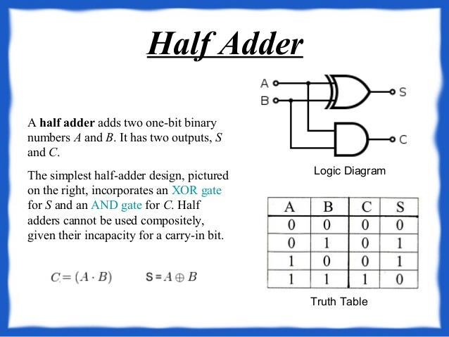
75 Half Adder Half adder is a combinational logic circuit with two inputs and two outputs. It is a basic building block for addition of two single bit numbers. Inputs A B Half Adder Sum Carry Outputs 8/29/
76
77 Half Adder K-map for Sum Output: B B A B A A S AB AB S A B K-map for Carry Output: A A A B 0 1 B C AB B /29/
78 Half Adder Logic Diagram: A B S A B C AB 8/29/
79 Half Adder Logic Diagram using Basic Gates: A B S A B C AB 8/29/
80 Full Adder Full adder is a combinational logic circuit with three inputs and two outputs. A Sum Inputs B Full Outputs Adder Carry Cin 8/29/
81 TRUTH TABLE
82 Full Adder K-map for Sum Output: A A BC BC BC BC BC A S ABC ABC ABC ABC S ABC ABC ABC ABC S C( AB AB) C( AB AB) ABC ABC ABC ABC Let AB AB X S C( X ) C( X ) S C X Let X A B S C A B 8/29/
83 Full Adder K-map for Carry Output: A A BC BC BC BC BC A C AB BC AC AC BC AB 8/29/
84 Full Adder Logic Diagram: A B C S A B C C AB BC AC 8/29/
85 Full Adder using Half Adders A B HA1 S 0 S 1 HA2 C 0 C 1 Sum C Carry 8/29/
86 Half Subtractor Half subtractor is a combinational logic circuit with two inputs and two outputs. It is a basic building block for subtraction of two single bit numbers. Inputs A B Half Subtractor Difference Borrow Outputs 8/29/
87 HALF SUBSTRACTOR
88 Half Subtractor K-map for Difference Output: B B A B A A D AB AB D A B K-map for Borrow Output: A A A B 0 1 B B AB B /29/
89 Half Subtractor Logic Diagram: A B D A B B AB 8/29/
90 Half Subtractor Logic Diagram using Basic Gates: A B D A B B AB 8/29/
91 Full Subtractor Full subtractor is a combinational logic circuit with three inputs and two outputs. A Difference Inputs B Full Outputs Subtractor Borrow Bin 8/29/
92 FULL SUBSTRATOR
93 Full Subtractor K-map for Difference Output: A A BC BC BC BC BC A D ABC ABC ABC ABC D ABC ABC ABC ABC D C( AB AB) C( AB AB) ABC ABC ABC ABC Let AB AB X D C( X ) C( X ) D C X Let X A B D C A B 8/29/
94 Full Subtractor K-map for Borrow Output: A A BC BC BC BC BC A B0 AB BC AC AC BC AB 8/29/
95 Full Subtractor Logic Diagram: A B C D A B C B0 AB BC AC 8/29/
96 Full Subtractor using Half Subtractor A B HS1 D 0 D 1 HS2 B 0 B 1 Difference C Borrow 8/29/
97 Combinational Logic Circuits Introduction Standard representation of canonical forms (SOP & POS), Maxterm and Minterm, Conversion between SOP and POS forms K-map reduction techniques upto 4 variables (SOP & POS form), Design of Half Adder, Full Adder, Half Subtractor & Full Subtractor using k-map Code Converter using K-map: Gray to Binary, Binary to Gray Code Converter (upto 4 bit) IC 7447 as BCD to 7- Segment decoder driver IC 7483 as Adder & Subtractor, 1 Digit BCD Adder Block Schematic of ALU IC IC /29/
98 Seven Segment Display a f e g b c d dp 8/29/
99 Seven Segment Display Segments a b c d e f g Display Number Seven Segment Display ON ON ON ON ON ON OFF 0 OFF ON ON OFF OFF OFF OFF 1 ON ON OFF ON ON OFF ON 2 ON ON ON ON OFF OFF ON 3 OFF ON ON OFF OFF ON ON 4 ON OFF ON ON OFF ON ON 5 ON OFF ON ON ON ON ON 6 ON ON ON OFF OFF OFF OFF 7 ON ON ON ON ON ON ON 8 ON ON ON ON OFF ON ON 9 8/29/2017 Amit Nevase 99
100 Types of Seven Segment Display Common Cathode Display Common Anode Display 8/29/
101 Common Anode Display +Vcc R R R R R R R R a b c d e f g dp 8/29/
102 Common Anode Display +Vcc BCD Input BCD to 7 Segment Decoder a b c d e f g R R R R R R R R 8/29/ dp
103 Common Cathode Display a b c d e f g dp R R R R R R R R 8/29/
104 R R R R R R R R Common Cathode Display a b c BCD Input BCD to 7 Segment Decoder d e f g 8/29/ dp
105 BCD to 7 Segment Decoder Driver ICs Sr. No. IC Number Specifications 1 IC 7446, IC Active Low open collector outputs, maximum voltage 30 V, maximum current sinking capability 40mA 2 IC 7447, IC Active Low open collector outputs, maximum voltage 15 V, maximum current sinking capability 40mA 3 IC 7448, IC Active High open collector outputs, Pull up resistor 2kohm, maximum voltage 5.5 V, maximum current sinking capability 6.4mA 8/29/

106 IC 7447 Pins A,B,C,D Description BCD Inputs a to g LT RBI BI Active Low Outputs Lamp Test Ripple Blanking Input Blanking Input RBO Ripple Blanking output 8/29/
107 RBI - Ripple Blanking Input For the normal decoding operation, this input should be connected to logic 1. If RBI is connected to ground, then it switches off the display when BCD inputs corresponding to 0. For non-zero BCD inputs, the decoder output will be normal and the BCD number will be displayed. RBI=0 is connected for blanking out the 8/29/ leading zeros in multidigit displays.
108 BI Blanking Input If BI is connected to 0, then the display will be switched off irrespective of the BCD input. This feature is used in the multiplexed display in order to save power. In the non-multiplexed displays this input is permanently connected to Vcc 8/29/
109 RBO Ripple Blanking Output This output is normally at logic 1. But it goes to logic 0 during the zero blanking interval when RBI is forced to a low level. RBO is used for cascading purpose and it is connected to RBI of the next stage. 8/29/
110 LT - Lamp Test This pin can be used to check whether all the segments of the display are working properly or not. If LT is forced low with RBO at logic 1 or open, then all the output terminals will be forced to their active state 8/29/
111 Circuit Diagram 8/29/ a b c d e f g dp R R R R R R R BCD Inputs LSB MSB IC 7447 a b c d e f g dp LT RBI / BI RBO Vcc Gnd A0 A1 A2 A3 5V a b c d e f g Common


112 Display Configuration LTS 542 Common g f a b f e a g b c d dp e d c dp Common 8/29/

113 Display Configuration 8/29/
114 Combinational Logic Circuits Introduction Standard representation of canonical forms (SOP & POS), Maxterm and Minterm, Conversion between SOP and POS forms K-map reduction techniques upto 4 variables (SOP & POS form), Design of Half Adder, Full Adder, Half Subtractor & Full Subtractor using k-map Code Converter using K-map: Gray to Binary, Binary to Gray Code Converter (upto 4 bit) IC 7447 as BCD to 7- Segment decoder driver IC 7483 as Adder & Subtractor, 1 Digit BCD Adder Block Schematic of ALU IC IC /29/
115 N Bit Parallel Adder The full adder is capable of adding two single digit binary numbers along with a carry input. But in practice we need to add binary numbers which are much longer than one bit. To add two n-bit binary numbers we need to use the n-bit parallel adder. It uses a number of full adders in cascade. The carry output of the previous full adder is connected to the carry input of the next full adder.. 8/29/
116 N Bit Parallel Adder A1 An 1 Bn 1 A2 B2 B1 A0 B0 FA-(n-1) FA-2 FA-1 FA-0 0 Cin Sn 1 S 2 S1 S 0 8/29/
117 4 Bit Parallel Adder using full adder A1 A3 B3 A2 B2 B1 A0 0 B C 0 FA-3 FA-2 FA-1 FA-0 Cin S 3 S 2 S1 S 0 8/29/
118 IC Bit Binary Parallel Adder A1 A3 B3 A2 B2 B1 A0 0 B C 0 FA-3 FA-2 FA-1 FA-0 Cin S 3 S 2 S1 S 0 8/29/
119 IC Bit Binary Parallel Adder A Binary number B Binary number A3 A2 A1 A0 B3 B2 B1 0 B C 0 Carry Output IC 7483 Cin Carry Input S 3 S 2 S1 S 0 Sum Output 8/29/
120 Cascading of IC 7483 If we want to add two 8 bit binary numbers using 4 bit binary parallel adder IC 7483, then we have to cascade the two ICs in following way Higher nibble of Higher nibble of A Binary number B Binary number A7 A6 A5 A4 B7 B6 B5 4 B Lower nibble of Lower nibble of A Binary number B Binary number A3 A2 A1 A0 B3 B2 B1 0 B C 0 IC 7483-II Cin C 0 IC 7483-I Cin Carry Carry Output Input S 7 S 6 S 5 S 4 S 3 S 2 S1 S 0 Sum Output 8/29/
121 Design of 1 Digit BCD Adder Block Diagram: A BCD no. B BCD no. C 0 IC 7483-I S 3 S 2 S1 S 0 Cin Logic Circuit Add 0110 Command C 0 IC 7483-II Cin S S 2 1 8/29/ S S 0 121
122 Design of 1 Digit BCD Adder As we know BCD addition rules, we understand that the 4 bit BCD adder should consists of following: A 4 bit binary adder to add the given two (4 bit numbers). A combinational logic circuit to check if sum is greater than 9 or carry 1. One more 4 bit binary adder to add 0110 to the invalid BCD sum or if carry is 1 8/29/
123 Design of 1 Digit BCD Adder Logic Table for design of Logic circuit: Inputs Y Inputs Y S 3 S 2 S 1 S S 3 S 2 S 1 S Sum is invalid BCD Number /29/2017 Amit Nevase 123 Y=1
124 Design of 1 Digit BCD Adder K-map for Logic circuit: S 3 s 2 SS 3 2 S 1 S 0 00 SS 1 0 SS 1 0 SS 1 0 SS SS SS Y S 3S 2 S 3S1 SS SS 3 2 SS 1 3 8/29/
125
126 4-BIT BCD ADDER
127 4 Bit Binary Parallel Subtractor using IC 7483 A Binary number B Binary number A3 A2 A1 A0 B3 B2 B1 0 B NOT gates for 1 s complement of B Vcc 5V C 0 Carry S 3 S 2 IC 7483 Output S1 It adds 1 to 1 s S 0 Cin 1 complement of B Difference Output 8/29/
128 IC 7483 as Parallel Adder/Subtractor B Binary number A Binary number A3 A2 A1 A0 B3 B2 B1 B0 M Mode Select C 0 Carry IC 7483 Cin Output S 3 S 2 S1 S 0 Sum or Difference Output Mode Select M=0 Addition M=1 Subtraction 8/29/

129 IC comparators provide outputs to indicate which of the numbers is larger or if they are equal. The bits are numbered starting at 0, rather than 1 as in the case of adders. Comparators Cascading inputs Cascading inputs are provided to expand the comparator to larger numbers. A 0 A 1 A 2 A 3 B 0 B 1 B 2 B 3 COMP 0 A 3 A > B A > B A = B A = B A < B A < B 0 A 3 Outputs The IC shown is the 4-bit 74HC85/74LS85.
130 74LS85 (4 bit magnitude comparator) The 74LS85 compares two unsigned 4-bit binary numbers, the unsigned numbers are A 3, A 2, A 1, A 0 and B 3, B 2, B 1, B 0. Cascading Inputs Outputs 130

131 Comparators Use 74HC85 comparators to compare the magnitudes of two 8-bit numbers. Show the comparators with proper interconnections. A=A7A6A5A4A3A2A1A0 and B=B 7 B 6 B 5 B 4 B 3 B 2 B 1 B 0 IC comparators can be expanded using the cascading inputs as shown. The lowest order comparator has a HIGH on the A = B input V LSBs A 0 A 1 A 2 A 3 B 0 B 1 B 2 B 3 COMP 0 A 3 A > B A > B A = B A = B A < B A < B 0 A 3 MSBs A 4 A 5 A 6 A 7 B 4 B 5 B 6 B 7 COMP 0 A 3 A > B A > B A = B A = B A < B A < B 0 A 3 Outputs
132 Combinational Logic Circuits Introduction Standard representation of canonical forms (SOP & POS), Maxterm and Minterm, Conversion between SOP and POS forms K-map reduction techniques upto 4 variables (SOP & POS form), Design of Half Adder, Full Adder, Half Subtractor & Full Subtractor using k-map Code Converter using K-map: Gray to Binary, Binary to Gray Code Converter (upto 4 bit) IC 7447 as BCD to 7- Segment decoder driver IC 7483 as Adder & Subtractor, 1 Digit BCD Adder Block Schematic of ALU IC 74181, IC /29/
133 IC Arithmetic Logic Unit A very popular & widely used combinational circuit is ALU which is capable of performing arithmetic as well as logical operation. Arithmetic Operating Modes: Addition Subtraction Shift Operation Magnitude Comparison 12 other arithmetic operations 8/29/
134 IC Logical Function Modes: Exclusive OR Comparator AND, NAND, OR, NOR 10 other arithmetic operations 8/29/

135 IC Pin Diagram 8/29/
136 IC Function Table 8/29/
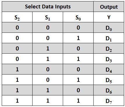
137 IC Bit Arithmetic Logic Unit Features: Low input loading minimizes drive requirements Performs six arithmetic and logic functions Selectable LOW (clear) and HIGH (preset) functions Carry generate and propagate outputs for use with carry look ahead generator 8/29/
138 IC Pin Configuration 8/29/
139 IC Function Table 8/29/
140 Combinational Logic Circuits Necessity, Applications and Realization of following Multiplexers (MUX): MUX Tree Demultiplexers (DEMUX): DEMUX Tree, DEMUX as Decoder Study of IC 74151, IC Priority Encoder 8:3, Decimal to BCD Encoder Tristate Logic, Unidirectional & Bidirectional buffer ICs: IC and IC /29/
141 Multiplexers Multiplexer is a circuit which has a number of inputs but only one output. Multiplexer is a circuit which transmits large number of information signals over a single line. Multiplexer is also known as Data Selector or MUX. 8/29/
142 Necessity of Multiplexers In most of the electronic systems, the digital data is available on more than one lines. It is necessary to route this data over a single line. Under such circumstances we require a circuit which select one of the many inputs at a time. This circuit is nothing but a multiplexer. Which has many inputs, one output and some select lines. Multiplexer improves the reliability of the digital system because it reduces the number 8/29/
143 Advantages of Multiplexers It reduces the number of wires. So it reduces the circuit complexity and cost. We can implement many combinational circuits using Mux. It simplifies the logic design. It does not need the k-map and simplification. 8/29/
144 Applications of Multiplexers It is used as a data selector to select one out of many data inputs. It is used for simplification of logic design. It is used in data acquisition system. In designing the combinational circuits. In D to A converters. To minimize the number of connections. 8/29/
145 Block Diagram of Multiplexer D 0 D 0 Data Inputs D 1 D 2 D 3... n:1 Mux Y Output D 1 D 2 D 3... Output D n-1 E Enable Input D n S m-1 S 2 S 1 s 0 S m-1 S 2 S 1 s 0 Select Lines Fig. General Block Diagram Fig. Equivalent Circuit 8/29/
146 Relation between Data Input Lines & Select Lines In general multiplexer contains, n data lines, one output line and m select lines. To select n inputs we need m select lines such that 2 m =n. 8/29/
147 Types of Multiplexers 2:1 Multiplexer 4:1 Multiplexer 8:1 Multiplexer 16:1 Multiplexer 32:1 Multiplexer 64:1 Multiplexer and so on 8/29/
148 2:1 Multiplexer Data Inputs D 0 D 1 E 2:1 Mux Y Output Block Diagram Enable Input s Select Lines Enable i/p (E) Select i/p (S) Output (Y) 0 X 0 Truth Table 1 0 D D 1 8/29/
149 Realization of 2:1 Mux using gates S D 1 D 0 S SD0 Y Output SD1 E Enable Input 8/29/
150 4:1 MULTIPLEXER
151 Realization of 4:1 Mux using gates S 1 S 0 S1S 0D0 D 0 S1S 0D1 D 1 D 2 S1S 0D2 Y Output D 3 S1S 0D3 E Enable Input 8/29/
152 16:1 Multiplexer D 0 D 1 D 2 D 3 Data Inputs D 4 D 5 D 6 D 7 D 8 D 9 D 10 D 11 D 12 D 13 D 14 D 15 16:1 Mux Y Output Block Diagram E Enable Input S 3 S 2 S 1 S 0 8/29/ Select Lines
153 Mux Tree The multiplexers having more number of inputs can be obtained by cascading two or more multiplexers with less number of inputs. This is called as Multiplexer Tree. For example, 32:1 mux can be realized using two 16:1 mux and one 2:1 mux. 8/29/
154 8:1 Multiplexer using 4:1 Multiplexer D 0 D 1 D 2 D 3 4:1 Mux Y 1 Select S 2 E S 1 S 0 Y Lines S 1 S 0 S 1 S 0 Output D 4 D 5 D 6 D 7 4:1 Mux Y 2 E 8/29/
155 8:1 Multiplexer using 4:1 Multiplexer D 0 D 1 D 2 D 3 4:1 Mux Y 1 S 1 S 0 E S 1 S 1 S 0 S 0 D 0 D 1 E 2:1 Mux Y Output D 4 D 5 4:1 S 2 D 6 Mux Y 2 D 7 E 8/29/
156 D 0 D 1 D 2 D 3 S 1 4:1 Mux S 0 Y 1 16:1 Mux using 4:1 Mux S 1 S 0 D 4 D 5 D 6 D 7 D 8 D 9 D 10 D 11 S 1 S 1 4:1 Mux 4:1 Mux S 0 S 0 Y 2 Y 3 D 0 D 1 D 2 D 3 S 1 S 3 4:1 Mux S 0 S 2 Y Output D 12 S 1 S 0 D 4:1 13 Y 4 D 14 Mux 8/29/2017 D
157 Realization of Boolean expression using Mux We can implement any Boolean expression using Multiplexers. It reduces circuit complexity. It does not require any simplification 8/29/
158 Example 1 Implement following Boolean expression using multiplexer f ( A, B, C) m(0,3,5,6) Since there are three variables, therefore a multiplexer with three select input is required i.e. 8:1 multiplexer is required The 8:1 multiplexer is configured as below to implement given Boolean expression 8/29/
159 Example 1 continue.. +V cc f ( A, B, C) m(0,3,5,6) D 0 D 1 D 2 D 3 D 4 D 5 8:1 Mux Y Output D 6 D 7 E S 2 S 1 S 0 A B C 8/29/
160 Example 2 Implement following Boolean expression using multiplexer f ( A, B, C, D) m(0,2,3,6,8,9,12,14) Since there are four variables, therefore a multiplexer with four select input is required i.e. 16:1 multiplexer is required The 16:1 multiplexer is configured as below to implement given Boolean expression 8/29/
161 Example 2 continue.. +V cc f ( A, B, C, D) m(0,2,3,6,8,9,12,14) D 0 D 1 D 2 D 3 D 4 D 5 D 6 D 7 D 8 D 9 D 10 D 11 D 12 D 13 D 14 D 15 16:1 Mux Y Output E S 3 S 2 S 1 S 0 A B C 8/29/ D
162 Combinational Logic Circuits Necessity, Applications and Realization of following Multiplexers (MUX): MUX Tree Demultiplexers (DEMUX): DEMUX Tree, DEMUX as Decoder Study of IC 74151, IC Priority Encoder 8:3, Decimal to BCD Encoder Tristate Logic, Unidirectional & Bidirectional buffer ICs: IC and IC /29/
163 De-multiplexer A de-multiplexer performs the reverse operation of a multiplexer i.e. it receives one input and distributes it over several outputs. At a time only one output line is selected by the select lines and the input is transmitted to the selected output line. It has only one input line, n number of output lines and m number of select lines. 8/29/
164 Block Diagram of De-multiplexer Y 0 Y 0 Y 1 Y 1 Data Input 1:n De-mux... Y 2 Y 3 Outputs Data Input... Y 2 Y 3 Outputs. Y n-1. Y n-1 E.. Enable Input S m-1 S 2 S 1 s 0 S m-1 S 2 S 1 s 0 Select Lines Fig. General Block Diagram Fig. Equivalent Circuit 8/29/
165 Relation between Data Output Lines & Select Lines In general de-multiplexer contains, n output lines, one input line and m select lines. To select n outputs we need m select lines such that n=2 m. 8/29/
166 Types of De-multiplexers 1:2 De-multiplexer 1:4 De-multiplexer 1:8 De-multiplexer 1:16 De-multiplexer 1:32 De-multiplexer 1:64 De-multiplexer and so on 8/29/

167 1:2 De-mux
168 1:2 De-mux using basic gates E D in S S Y 0 Y 1 8/29/

169 1:4 De-mux
170 1:4 De-mux using basic gates E D in S1 S 0 S1 S 0 Y 0 Y 1 Y 2 Y 3 8/29/
171 1: 8 De-multiplexer Data D in Input E Enable Input 1:8 De-mux S 2 S 1 S 0 Select Lines Block Diagram Y 0 Y 1 Y 2 Y 3 Y 4 Y 5 Y 6 Y 7 8/29/
172 1: 16 De-multiplexer Block Diagram Data Input E D in Enable Input 1:16 De-mux 8/29/2017 S S S 2 S 1 0 Y 0 Y 1 Y 2 Y 3 Y 4 Y 5 Y 6 Y 7 Y 8 Y 9 Y 10 Y 11 Y 12 Y 13 Y 14 Y 15
173 De-mux Tree Similar to multiplexer we can construct the de-multiplexer with more number of lines using de-multiplexer having less number of lines. This is call as De-mux Tree. 8/29/
174 1:4 De-mux using 1:2 De-mux Data Input Select S 1 D in E 1:2 De-mux S 0 Y 0 Y 1 Y 0 Y 1 Lines S 0 D in E S 0 1:2 De-mux Y 0 Y 1 Y 2 Y 3 8/29/
175 1:16 De-mux using 1:4 De-mux D in S 1 1:4 De-mux S 0 Y 0 Y 1 Y 2 Y 3 Data Input D in 1:4 De-mux S 1 S 0 Y 0 Y 1 Y 2 Y 3 D in S 1 S 0 1:4 De-mux Y 4 Y 5 Y 6 Y 7 S 3 S 2 D in S 1 1:4 De-mux S 0 Y 8 Y 9 Y 10 Y 11 D in Y 14 S 1 S 0 8/29/2017 De-mux Y S 1 1:4 S 0 Y 12 Y 13
176 Decoder Decoder is a combinational circuit. It converts n bit binary information at its input into a maximum of 2 n output lines. For example, if n=2 then we can design upto 2:4 decoder 8/29/
177 De-multiplexer as Decoder It is possible to operate a de-multiplexer as a decoder. Let us consider an example of 1:4 de-mux can be used as 2:4 decoder 8/29/
178 1:4 De-multiplexer as 2:4 Decoder V cc Data Input E D in 1:4 De-mux Y 0 Y 1 Y 2 Y 3 Inputs A B S 1 S 0 D in 1:4 De-mux Y 0 Y 1 Y 2 Y 3 Enable Input S 1 S 0 Select Lines E Enable Input 1: 4 De-multiplexer 1: 4 De-multiplexer as 2:4 Decoder 8/29/
179 Realization of Boolean expression using De-mux We can implement any Boolean expression using de-multiplexers. It reduces circuit complexity. It does not require any simplification 8/29/
180 Example 1 Implement following Boolean expression using de-multiplexer f ( A, B, C) m(0,3,5,6) Since there are three variables, therefore a de-multiplexer with three select input is required i.e. 1:8 de-multiplexer is required The 1:8 de-multiplexer is configured as below to implement given Boolean expression 8/29/
181 Example 1 continue.. f ( A, B, C) m(0,3,5,6) +V cc Y 0 Data Input E Enable Input D in S 2 1:8 De-mux S 1 S 0 A B C Y 1 Y 2 Y 3 Y 4 Y 5 Y 6 Y 7 Y 8/29/
182 Example 2 Implement following Boolean expression using de-multiplexer f ( A, B, C, D) m(0,2,3,6,8,9,12,14) Since there are four variables, therefore a demultiplexer with four select input is required i.e. 1:16 de-multiplexer is required The 1:16 de-multiplexer is configured as below to implement given Boolean expression 8/29/
183 Example 2 continue.. Data E +V cc Input D in Enable Input 1:16 De-mux S 3 S 2 A B C S 1 D Y 0 Y 1 Y 2 Y 3 Y 4 Y 5 Y 6 Y 7 Y 8 Y 9 Y 10 Y 11 Y 12 Y 13 Y 14 SY 0 15 f ( A, B, C, D) m(0,2,3,6,8,9,12,14) 8/29/ Y
184 Module III Combinational Logic Circuits Necessity, Applications and Realization of following (8 Marks) Multiplexers (MUX): MUX Tree Demultiplexers (DEMUX): DEMUX Tree, DEMUX as Decoder Study of IC 74151, IC Priority Encoder 8:3, Decimal to BCD Encoder Tristate Logic, Unidirectional & Bidirectional buffer ICs: IC and IC /29/
185 Multiplexer ICs IC Number Description Output IC Quad 2:1 Mux Same as input IC Quad 2:1 Mux Inverted Output IC Dual 4:1 Mux Same as input IC Dual 4:1 Mux Inverted Output IC :1 Mux Inverted Output IC :1 Mux Inverted Output IC :1 Mux Inverted Output 8/29/
186 IC General Description This Data Selector/Multiplexer contains full on-chip decoding to select one-of-eight data sources as a result of a unique three-bit binary code at the Select inputs. Two complementary outputs provide both inverting and non-inverting buffer operation. Y A Strobe input is provided which, when at the high level, disables all data inputs and forces the Y output to the low state and the output to the high state. 8/29/
187 IC Features Advanced oxide-isolated, ion-implanted Schottky TTL process Switching performance is guaranteed over full temperature and VCC supply range Pin and functional compatible with LS family counterpart Improved output transient handling capability 8/29/
188 IC Pin Diagram V CC G ND D 0 D 1 D 2 Y Data Inputs D 3 D 4 D 5 8:1 Mux Y D 6 D 7 Pin Diagram E Enable Input Select Lines 8/29/ Equivalent Diagram S 2 S 1 S 0
189 De-multiplexer ICs IC Number Description IC :8 De-multiplexer IC Dual 1:4 De-multiplexer IC :16 De-multiplexer IC Dual 1:4 De-multiplexer 8/29/
190 IC General Description These monolithic TTL circuits feature dual 1 line to 4 line de-multiplexers with individual strobes and common binary address inputs in a single 16 pin package. The individual strobes permit activating or inhibiting each of the 4-bit sections as desired. 8/29/
191 8/29/ to 8 line de-multiplexer 191 IC Features Input clamping diodes simplify system design. Choice of outputs : Totem pole ( LS155A) or open collector ( LS156). Individual strobes simplify cascading for decoding or de-multiplexing larger words. Applications: Dual 2 to 4 Line Decoder Dual 1: 4 De-multiplexer 3 to 8 line Decoder

192 IC 7155 Pin Diagram 8/29/
193 Combinational Logic Circuits Necessity, Applications and Realization of following (8 Marks) Multiplexers (MUX): MUX Tree Demultiplexers (DEMUX): DEMUX Tree, DEMUX as Decoder Study of IC 74151, IC Priority Encoder 8:3, Decimal to BCD Encoder Tristate Logic, Unidirectional & Bidirectional buffer ICs: IC and IC /29/
194 Encoder Encoder is a combinational circuit which is designed to perform the inverse operation of decoder. An encoder has n number of input lines and m number of output lines. An encoder produces an m bit binary code corresponding to the digital input number. The encoder accepts an n input digital word and converts it into m bit another digital word 8/29/
195 Encoder n inputs.. Encoder.. m outputs.. 8/29/
196 Types of Encoders Priority Encoder Decimal to BCD Encoder Octal to BCD Encoder Hexadecimal to Binary Encoder 8/29/
197 Priority Encoder This is a special type of encoder. Priorities are given to the input lines. If two or more input lines are 1 at the same time, then the input line with highest priority will be considered. 8/29/
198 Priority Encoder 8:3 Highest Priority 8 inputs D 0 D 1 D 2 D 3 D 4 D 5 D 6 D 7 Priority Encoder 8:3 Y 2 Y 1 Y 0 3 outputs Lowest Priority 8/29/
199
200 Decimal to BCD Encoder 9 inputs D 1 D 2 D 3 D 4 D 5 D 6 D 7 Decimal to BCD Encoder A B C D BCD outputs D 8 D 9 8/29/
201 Combinational Logic Circuits Necessity, Applications and Realization of following Multiplexers (MUX): MUX Tree Demultiplexers (DEMUX): DEMUX Tree, DEMUX as Decoder Study of IC 74151, IC Priority Encoder 8:3, Decimal to BCD Encoder Tristate Logic, Unidirectional & Bidirectional buffer ICs: IC and IC /29/
202 Tristate Logic In digital electronics three-state, tri-state, or 3-state logic allows an output port to assume a high impedance state in addition to the 0 and 1 logic levels, effectively removing the output from the circuit. 8/29/
203 Digital Buffer Sometimes in digital electronic circuits we need to isolate logic gates from each other or have them drive or switch higher than normal loads, such as relays, solenoids and lamps without the need for inversion. One type of single input logic gate that allows us to do just that is called the Digital Buffer. 8/29/
204 Digital Buffer Unlike the single input, single output inverter or NOT gate such as the TTL 7404 which inverts or complements its input signal on the output, the Buffer performs no inversion or decision making capabilities (like logic gates with two or more inputs) but instead produces an output which exactly matches that of its input. In other words, a digital buffer does nothing as its output state equals its input state. Then digital buffers can be regarded as Idempotent gates applying Boole s Idempotent Law because when an input passes through this device its value is not changed. So the digital buffer is a non-inverting device and will therefore give us the Boolean expression of: Q = A. 8/29/
205 Tri-state Buffer As well as the standard Digital Buffer seen above, there is another type of digital buffer circuit whose output can be electronically disconnected from its output circuitry when required. This type of Buffer is known as a 3-State Buffer or more commonly a Tri-state Buffer. A Tri-state Buffer can be thought of as an input controlled switch with an output that can be electronically turned ON or OFF by means of an external Control or Enable ( EN ) signal input. This control signal can be either a logic 0 or a logic 1 type signal resulting in the Tri-state Buffer being in one state allowing its output to operate normally producing the required output or in another state were its output is blocked or disconnected. 8/29/

206 Tri-state Buffer - Equivalent 8/29/
207 What is Parity Generator? A Parity Generator is a Combinational Logic Circuit that Generates the Parity bit in the Transmitter. A Parity bit is used for the Purpose of Detecting Errors during Transmissions of binary Information. It is an Extra bit Included with a binary Message to Make the Number of 1 s either Odd or Even.
208 Two Types of Parity In Even Parity, the added Parity bit will Make the Total Number of 1 s an Even Amount. In Odd Parity, the added Parity bit will Make the Total Number of 1 s an Odd Amount.

209 Parity Generator Truth Table and Logic Diagram 3-bit Message Odd X Y Z Parity Bit Even Parity Bit
210 Boolean Expression K-Map Simplification Even Pair P =XYZ + XYZ + XYZ + XYZ X YZ =X YZ + YZ + X YZ + YZ =X Y Z + X Y Z =X (Y Z) Odd Pair P =XYZ + XYZ + XYZ + XYZ =X YZ + YZ + X YZ + YZ =X Y Z + X Y Z =X (Y Z) YZ X
211 Parity Checker A Circuit that Checks the Parity in the Receiver is called Parity Checker. The Parity Checker Circuit Checks for Possible Errors in the Transmission. Since the Information Transmitted with Even Parity, the Received must have an even number of 1 s.if it has odd number of 1 s, it indicates that there is a Error occurred during Transmission. The Output of the Parity Checker is denoted by PEC(Parity Error Checker).If there is error, that is,if it has odd number of 1 s, it will indicate 1.If no then PEC will indicate 0.
212 Even Parity Checker Truth Table Decimal Equivalent Four Bits Received Parity Error P A B C PEC
213 Logic Diagram K-Map Simplification PA BC Boolean Expression PEC = PA BC + BC + PA BC + BC + PA BC + BC + PA (BC + BC) =PA B C + PA B C + PA B C + PA B C =(PA + PA) B C + PA + PA B C =(P A) B C + P A B C =(P A) (B C)
214 Bi-directional Buffer It is also possible to connect Tri-state Buffers back-to-back to produce what is called a Bi-directional Buffer circuit with one active-high buffer connected in parallel but in reverse with one active-low buffer. Here, the enable control input acts more like a directional control signal causing the data to be both read from and transmitted to the same data bus wire. In this type of application a tri-state buffer with bi-directional switching capability such as the TTL can be used. 8/29/

215 References Digital Principles by Malvino Leach Modern Digital Electronics by R.P. Jain Digital Electronics, Principles and Integrated Circuits by Anil K. Maini Digital Techniques by A. Anand Kumar 8/29/

216 Online Tutorials php?subjectid= n/comb_1.html n/comb_2.html 8/29/2017 Amit Nevase 216
217 Thank You 8/29/
Unit 3 Session - 9 Data-Processing Circuits
 Objectives Unit 3 Session - 9 Data-Processing Design of multiplexer circuits Discuss multiplexer applications Realization of higher order multiplexers using lower orders (multiplexer trees) Introduction
Logic. Combinational. inputs. outputs. the result. system can
 Digital Electronics Combinational Logic Functions Digital logic circuits can be classified as either combinational or sequential circuits. A combinational circuit is one where the output at any time depends
SIR C.R.REDDY COLLEGE OF ENGINEERING ELURU DIGITAL INTEGRATED CIRCUITS (DIC) LABORATORY MANUAL III / IV B.E. (ECE) : I - SEMESTER
 LABORATORY MANUAL III / IV B.E. (ECE) : I - SEMESTER") SIR C.R.REDDY COLLEGE OF ENGINEERING ELURU 534 007 DIGITAL INTEGRATED CIRCUITS (DIC) LABORATORY MANUAL III / IV B.E. (ECE) : I - SEMESTER DEPARTMENT OF ELECTRONICS AND COMMUNICATION ENGINEERING DIGITAL
SIR C.R.REDDY COLLEGE OF ENGINEERING ELURU 534 007 DIGITAL INTEGRATED CIRCUITS (DIC) LABORATORY MANUAL III / IV B.E. (ECE) : I - SEMESTER DEPARTMENT OF ELECTRONICS AND COMMUNICATION ENGINEERING DIGITAL
Digital Electronics Circuits 2017
 JSS SCIENCE AND TECHNOLOGY UNIVERSITY Digital Electronics Circuits (EC37L) Lab in-charge: Dr. Shankraiah Course outcomes: After the completion of laboratory the student will be able to, 1. Simplify, design
UNIT II COMBINATIONAL CIRCUITS:
 UNIT II COMBINATIONAL CIRCUITS: INTRODUCTION: The digital system consists of two types of circuits, namely (i) (ii) Combinational circuits Sequential circuits Combinational circuit consists of logic gates
COMBINATIONAL LOGIC FUNCTIONS
 COMBINATIONAL LOGIC FUNCTIONS Digital logic circuits can be classified as either combinational or sequential circuits. A combinational circuit is one where the output at any time depends only on the present
Minimization techniques
 Pune Vidyarthi Griha s COLLEGE OF ENGINEERING, NSIK - 4 Minimization techniques By Prof. nand N. Gharu ssistant Professor Computer Department Combinational Logic Circuits Introduction Standard representation
Sample Test Paper - I
 Scheme G Sample Test Paper - I Course Name : Computer Engineering Group Marks : 25 Hours: 1 Hrs. Q.1) Attempt any THREE: 09 Marks a) Define i) Propagation delay ii) Fan-in iii) Fan-out b) Convert the following:
Combinational Logic. Mantıksal Tasarım BBM231. section instructor: Ufuk Çelikcan
 Combinational Logic Mantıksal Tasarım BBM23 section instructor: Ufuk Çelikcan Classification. Combinational no memory outputs depends on only the present inputs expressed by Boolean functions 2. Sequential
MODULAR CIRCUITS CHAPTER 7
 CHAPTER 7 MODULAR CIRCUITS A modular circuit is a digital circuit that performs a specific function or has certain usage. The modular circuits to be introduced in this chapter are decoders, encoders, multiplexers,
Digital System Design Combinational Logic. Assoc. Prof. Pradondet Nilagupta
 Digital System Design Combinational Logic Assoc. Prof. Pradondet Nilagupta pom@ku.ac.th Acknowledgement This lecture note is modified from Engin112: Digital Design by Prof. Maciej Ciesielski, Prof. Tilman
( c) Give logic symbol, Truth table and circuit diagram for a clocked SR flip-flop. A combinational circuit is defined by the function
 Give logic symbol, Truth table and circuit diagram for a clocked SR flip-flop. A combinational circuit is defined by the function") Question Paper Digital Electronics (EE-204-F) MDU Examination May 2015 1. (a) represent (32)10 in (i) BCD 8421 code (ii) Excess-3 code (iii) ASCII code (b) Design half adder using only NAND gates. ( c)
Question Paper Digital Electronics (EE-204-F) MDU Examination May 2015 1. (a) represent (32)10 in (i) BCD 8421 code (ii) Excess-3 code (iii) ASCII code (b) Design half adder using only NAND gates. ( c)
S.Y. Diploma : Sem. III [DE/ED/EI/EJ/EN/ET/EV/EX/IC/IE/IS/IU/MU] Principles of Digital Techniques
![S.Y. Diploma : Sem. III [DE/ED/EI/EJ/EN/ET/EV/EX/IC/IE/IS/IU/MU] Principles of Digital Techniques](/thumbs/82/86792063.jpg "S.Y. Diploma : Sem. III [DE/ED/EI/EJ/EN/ET/EV/EX/IC/IE/IS/IU/MU] Principles of Digital Techniques") S.Y. Diploma : Sem. III [DE/ED/EI/EJ/EN/ET/EV/EX/IC/IE/IS/IU/MU] Principles of Digital Techniques Time: 3 Hrs.] Prelim Question Paper Solution [Marks : 100 Q.1(a) Attempt any SIX of the following : [12]
S.Y. Diploma : Sem. III [DE/ED/EI/EJ/EN/ET/EV/EX/IC/IE/IS/IU/MU] Principles of Digital Techniques Time: 3 Hrs.] Prelim Question Paper Solution [Marks : 100 Q.1(a) Attempt any SIX of the following : [12]
Chapter 4. Combinational: Circuits with logic gates whose outputs depend on the present combination of the inputs. elements. Dr.
 Chapter 4 Dr. Panos Nasiopoulos Combinational: Circuits with logic gates whose outputs depend on the present combination of the inputs. Sequential: In addition, they include storage elements Combinational
Lecture 2 Review on Digital Logic (Part 1)
") Lecture 2 Review on Digital Logic (Part 1) Xuan Silvia Zhang Washington University in St. Louis http://classes.engineering.wustl.edu/ese461/ Grading Engagement 5% Review Quiz 10% Homework 10% Labs 40%
Lecture 2 Review on Digital Logic (Part 1) Xuan Silvia Zhang Washington University in St. Louis http://classes.engineering.wustl.edu/ese461/ Grading Engagement 5% Review Quiz 10% Homework 10% Labs 40%
ELCT201: DIGITAL LOGIC DESIGN
 ELCT2: DIGITAL LOGIC DESIGN Dr. Eng. Haitham Omran, haitham.omran@guc.edu.eg Dr. Eng. Wassim Alexan, wassim.joseph@guc.edu.eg Lecture 4 Following the slides of Dr. Ahmed H. Madian محرم 439 ه Winter 28
Department of Electrical & Electronics EE-333 DIGITAL SYSTEMS
 Department of Electrical & Electronics EE-333 DIGITAL SYSTEMS 1) Given the two binary numbers X = 1010100 and Y = 1000011, perform the subtraction (a) X -Y and (b) Y - X using 2's complements. a) X = 1010100
CSE140: Components and Design Techniques for Digital Systems. Decoders, adders, comparators, multipliers and other ALU elements. Tajana Simunic Rosing
 CSE4: Components and Design Techniques for Digital Systems Decoders, adders, comparators, multipliers and other ALU elements Tajana Simunic Rosing Mux, Demux Encoder, Decoder 2 Transmission Gate: Mux/Tristate
Systems I: Computer Organization and Architecture
 Systems I: Computer Organization and Architecture Lecture 6 - Combinational Logic Introduction A combinational circuit consists of input variables, logic gates, and output variables. The logic gates accept
Number System. Decimal to binary Binary to Decimal Binary to octal Binary to hexadecimal Hexadecimal to binary Octal to binary
 Number System Decimal to binary Binary to Decimal Binary to octal Binary to hexadecimal Hexadecimal to binary Octal to binary BOOLEAN ALGEBRA BOOLEAN LOGIC OPERATIONS Logical AND Logical OR Logical COMPLEMENTATION
CHAPTER1: Digital Logic Circuits Combination Circuits
 CS224: Computer Organization S.KHABET CHAPTER1: Digital Logic Circuits Combination Circuits 1 PRIMITIVE LOGIC GATES Each of our basic operations can be implemented in hardware using a primitive logic gate.
IT T35 Digital system desigm y - ii /s - iii
 UNIT - II Combinational Logic Adders subtractors code converters binary parallel adder decimal adder magnitude comparator encoders decoders multiplexers demultiplexers-binarymultiplier Parity generator
KUMARAGURU COLLEGE OF TECHNOLOGY COIMBATORE
 Estd-1984 KUMARAGURU COLLEGE OF TECHNOLOGY COIMBATORE 641 006 QUESTION BANK UNIT I PART A ISO 9001:2000 Certified 1. Convert (100001110.010) 2 to a decimal number. 2. Find the canonical SOP for the function
Function of Combinational Logic ENT263
 Function of Combinational Logic ENT263 Chapter Objectives Distinguish between half-adder and full-adder Use BCD-to-7-segment decoders in display systems Apply multiplexer in data selection Use decoders
DHANALAKSHMI COLLEGE OF ENGINEERING, CHENNAI DEPARTMENT OF COMPUTER SCIENCE AND ENGINEERING CS6201 DIGITAL PRINCIPLES AND SYSTEM DESIGN
 DHANALAKSHMI COLLEGE OF ENGINEERING, CHENNAI DEPARTMENT OF COMPUTER SCIENCE AND ENGINEERING CS6201 DIGITAL PRINCIPLES AND SYSTEM DESIGN UNIT I : BOOLEAN ALGEBRA AND LOGIC GATES PART - A (2 MARKS) Number
Combinational Logic. By : Ali Mustafa
 Combinational Logic By : Ali Mustafa Contents Adder Subtractor Multiplier Comparator Decoder Encoder Multiplexer How to Analyze any combinational circuit like this? Analysis Procedure To obtain the output
Chapter 4: Combinational Logic Solutions to Problems: [1, 5, 9, 12, 19, 23, 30, 33]
![Chapter 4: Combinational Logic Solutions to Problems: [1, 5, 9, 12, 19, 23, 30, 33]](/thumbs/81/84077758.jpg "Chapter 4: Combinational Logic Solutions to Problems: [1, 5, 9, 12, 19, 23, 30, 33]") Chapter 4: Combinational Logic Solutions to Problems: [, 5, 9, 2, 9, 23, 3, 33] Problem: 4- Consider the combinational circuit shown in Fig. P4-. (a) Derive the Boolean expressions for T through T 4. Evaluate
Chapter 4: Combinational Logic Solutions to Problems: [, 5, 9, 2, 9, 23, 3, 33] Problem: 4- Consider the combinational circuit shown in Fig. P4-. (a) Derive the Boolean expressions for T through T 4. Evaluate
UNIT 1. BOOLEAN ALGEBRA AND COMBINATIONAL CIRCUITS
 UNIT 1. BOOLEAN ALGEBRA AND COMBINATIONAL CIRCUITS Numerical Presentation: In science, technology, business, and, in fact, most other fields of endeavour, we are constantly dealing with quantities. Quantities
Z = F(X) Combinational circuit. A combinational circuit can be specified either by a truth table. Truth Table
 Combinational circuit. A combinational circuit can be specified either by a truth table. Truth Table") Lesson Objectives In this lesson, you will learn about What are combinational circuits Design procedure of combinational circuits Examples of combinational circuit design Combinational Circuits Logic circuit
Lesson Objectives In this lesson, you will learn about What are combinational circuits Design procedure of combinational circuits Examples of combinational circuit design Combinational Circuits Logic circuit
Chap 2. Combinational Logic Circuits
 Overview 2 Chap 2. Combinational Logic Circuits Spring 24 Part Gate Circuits and Boolean Equations Binary Logic and Gates Boolean Algebra Standard Forms Part 2 Circuit Optimization Two-Level Optimization
211: Computer Architecture Summer 2016
 211: Computer Architecture Summer 2016 Liu Liu Topic: Storage Project3 Digital Logic - Storage: Recap - Review: cache hit rate - Project3 - Digital Logic: - truth table => SOP - simplification: Boolean
Computer Science 324 Computer Architecture Mount Holyoke College Fall Topic Notes: Digital Logic
 Computer Science 324 Computer Architecture Mount Holyoke College Fall 2007 Topic Notes: Digital Logic Our goal for the next few weeks is to paint a a reasonably complete picture of how we can go from transistor
Digital Techniques. Figure 1: Block diagram of digital computer. Processor or Arithmetic logic unit ALU. Control Unit. Storage or memory unit
 Digital Techniques 1. Binary System The digital computer is the best example of a digital system. A main characteristic of digital system is its ability to manipulate discrete elements of information.
CSE 140 Lecture 11 Standard Combinational Modules. CK Cheng and Diba Mirza CSE Dept. UC San Diego
 CSE 4 Lecture Standard Combinational Modules CK Cheng and Diba Mirza CSE Dept. UC San Diego Part III - Standard Combinational Modules (Harris: 2.8, 5) Signal Transport Decoder: Decode address Encoder:
CSE140: Components and Design Techniques for Digital Systems. Logic minimization algorithm summary. Instructor: Mohsen Imani UC San Diego
 CSE4: Components and Design Techniques for Digital Systems Logic minimization algorithm summary Instructor: Mohsen Imani UC San Diego Slides from: Prof.Tajana Simunic Rosing & Dr.Pietro Mercati Definition
Combinational Logic. Lan-Da Van ( 范倫達 ), Ph. D. Department of Computer Science National Chiao Tung University Taiwan, R.O.C.
, Ph. D. Department of Computer Science National Chiao Tung University Taiwan, R.O.C.") Combinational Logic ( 范倫達 ), Ph. D. Department of Computer Science National Chiao Tung University Taiwan, R.O.C. Fall, 2017 ldvan@cs.nctu.edu.tw http://www.cs.nctu.edu.tw/~ldvan/ Combinational Circuits
Combinational Logic ( 范倫達 ), Ph. D. Department of Computer Science National Chiao Tung University Taiwan, R.O.C. Fall, 2017 ldvan@cs.nctu.edu.tw http://www.cs.nctu.edu.tw/~ldvan/ Combinational Circuits
Class Website:
 ECE 20B, Winter 2003 Introduction to Electrical Engineering, II LECTURE NOTES #5 Instructor: Andrew B. Kahng (lecture) Email: abk@ece.ucsd.edu Telephone: 858-822-4884 office, 858-353-0550 cell Office:
SUMMER 18 EXAMINATION Subject Name: Principles of Digital Techniques Model Answer Subject Code:
 Important Instructions to examiners: 1) The answers should be examined by key words and not as word-to-word as given in the model answer scheme. 2) The model answer and the answer written by candidate
Section 3: Combinational Logic Design. Department of Electrical Engineering, University of Waterloo. Combinational Logic
 Section 3: Combinational Logic Design Major Topics Design Procedure Multilevel circuits Design with XOR gates Adders and Subtractors Binary parallel adder Decoders Encoders Multiplexers Programmed Logic
ECE 545 Digital System Design with VHDL Lecture 1. Digital Logic Refresher Part A Combinational Logic Building Blocks
 ECE 545 Digital System Design with VHDL Lecture Digital Logic Refresher Part A Combinational Logic Building Blocks Lecture Roadmap Combinational Logic Basic Logic Review Basic Gates De Morgan s Law Combinational
DIGITAL TECHNICS. Dr. Bálint Pődör. Óbuda University, Microelectronics and Technology Institute
 DIGITAL TECHNICS Dr. Bálint Pődör Óbuda University, Microelectronics and Technology Institute 4. LECTURE: COMBINATIONAL LOGIC DESIGN: ARITHMETICS (THROUGH EXAMPLES) 2016/2017 COMBINATIONAL LOGIC DESIGN:
PG - TRB UNIT-X- DIGITAL ELECTRONICS. POLYTECHNIC-TRB MATERIALS
 SRIMAAN COACHING CENTRE-PG-TRB-PHYSICS- DIGITAL ELECTRONICS-STUDY MATERIAL-CONTACT: 8072230063 SRIMAAN PG - TRB PHYSICS UNIT-X- DIGITAL ELECTRONICS POLYTECHNIC-TRB MATERIALS MATHS/COMPUTER SCIENCE/IT/ECE/EEE
Binary addition (1-bit) P Q Y = P + Q Comments Carry = Carry = Carry = Carry = 1 P Q
 P Q Y = P + Q Comments Carry = Carry = Carry = Carry = 1 P Q") Digital Arithmetic In Chapter 2, we have discussed number systems such as binary, hexadecimal, decimal, and octal. We have also discussed sign representation techniques, for example, sign-bit representation
Digital Arithmetic In Chapter 2, we have discussed number systems such as binary, hexadecimal, decimal, and octal. We have also discussed sign representation techniques, for example, sign-bit representation
CHAPTER 7. Exercises 17/ / /2 2 0
 CHAPTER 7 Exercises E7. (a) For the whole part, we have: Quotient Remainders 23/2 /2 5 5/2 2 2/2 0 /2 0 Reading the remainders in reverse order, we obtain: 23 0 = 0 2 For the fractional part we have 2
Combinational Logic. Lan-Da Van ( 范倫達 ), Ph. D. Department of Computer Science National Chiao Tung University Taiwan, R.O.C.
, Ph. D. Department of Computer Science National Chiao Tung University Taiwan, R.O.C.") Combinational Logic ( 范倫達 ), Ph. D. Department of Computer Science National Chiao Tung University Taiwan, R.O.C. Fall, 2010 ldvan@cs.nctu.edu.tw http://www.cs.nctu.edu.tw/~ldvan/ Combinational Circuits
Combinational Logic ( 范倫達 ), Ph. D. Department of Computer Science National Chiao Tung University Taiwan, R.O.C. Fall, 2010 ldvan@cs.nctu.edu.tw http://www.cs.nctu.edu.tw/~ldvan/ Combinational Circuits
Design of Sequential Circuits
 Design of Sequential Circuits Seven Steps: Construct a state diagram (showing contents of flip flop and inputs with next state) Assign letter variables to each flip flop and each input and output variable
Review for Test 1 : Ch1 5
 Review for Test 1 : Ch1 5 October 5, 2006 Typeset by FoilTEX Positional Numbers 527.46 10 = (5 10 2 )+(2 10 1 )+(7 10 0 )+(4 10 1 )+(6 10 2 ) 527.46 8 = (5 8 2 ) + (2 8 1 ) + (7 8 0 ) + (4 8 1 ) + (6 8
S.Y. Diploma : Sem. III [CO/CM/IF/CD/CW] Digital Techniques
![S.Y. Diploma : Sem. III [CO/CM/IF/CD/CW] Digital Techniques](/thumbs/90/103932933.jpg "S.Y. Diploma : Sem. III [CO/CM/IF/CD/CW] Digital Techniques") S.Y. Diploma : Sem. III [CO/CM/IF/CD/CW] Digital Techniques Time: 3 Hrs.] Prelim Question Paper Solution [Marks : 100 Q.1(a) Attempt any SIX of the following : [12] Q.1(a) (i) Derive AND gate and OR gate
S.Y. Diploma : Sem. III [CO/CM/IF/CD/CW] Digital Techniques Time: 3 Hrs.] Prelim Question Paper Solution [Marks : 100 Q.1(a) Attempt any SIX of the following : [12] Q.1(a) (i) Derive AND gate and OR gate
 vidyarthiplus.com vidyarthiplus.com vidyarthiplus.com ANNA UNIVERSITY- COMBATORE B.E./ B.TECH. DEGREE EXAMINATION - JUNE 2009. ELECTRICAL & ELECTONICS ENGG. - FOURTH SEMESTER DIGITAL LOGIC CIRCUITS PART-A
Why digital? Overview. Number Systems. Binary to Decimal conversion
 Why digital? Overview It has the following advantages over analog. It can be processed and transmitted efficiently and reliably. It can be stored and retrieved with greater accuracy. Noise level does not
UNIVERSITI TENAGA NASIONAL. College of Information Technology
 UNIVERSITI TENAGA NASIONAL College of Information Technology BACHELOR OF COMPUTER SCIENCE (HONS.) FINAL EXAMINATION SEMESTER 2 2012/2013 DIGITAL SYSTEMS DESIGN (CSNB163) January 2013 Time allowed: 3 hours
Connection Diagram DECODIFICADORES. 74LS42 Decodificador BCD a decimal. Grado en Ingeniería Informática FUNDAMENTOS DE TECNOLIGÍA DE COMPUTADORES
 Grado en Ingeniería Informática DEPARTAMENTO DE AUTOMÁTICA ARQUITECTURA Y TECNOLOGÍA DE COMPUTADORES FUNDAMENTOS DE TECNOLIGÍA DE COMPUTADORES Circuitos combinacionales MSI DECODIFICADORES 74LS42 Decodificador
Vidyalankar S.E. Sem. III [CMPN] Digital Logic Design and Analysis Prelim Question Paper Solution
![Vidyalankar S.E. Sem. III [CMPN] Digital Logic Design and Analysis Prelim Question Paper Solution](/thumbs/90/103673562.jpg "Vidyalankar S.E. Sem. III [CMPN] Digital Logic Design and Analysis Prelim Question Paper Solution") . (a) (i) ( B C 5) H (A 2 B D) H S.E. Sem. III [CMPN] Digital Logic Design and Analysis Prelim Question Paper Solution ( B C 5) H (A 2 B D) H = (FFFF 698) H (ii) (2.3) 4 + (22.3) 4 2 2. 3 2. 3 2 3. 2 (2.3)
. (a) (i) ( B C 5) H (A 2 B D) H S.E. Sem. III [CMPN] Digital Logic Design and Analysis Prelim Question Paper Solution ( B C 5) H (A 2 B D) H = (FFFF 698) H (ii) (2.3) 4 + (22.3) 4 2 2. 3 2. 3 2 3. 2 (2.3)
COMBINATIONAL CIRCUITS
 OMINTIONL IRUITS pplications Parity Generation and heking Even Parity P e P e P P P P P P5 P P6 ( ) = m(,, ) =, Odd Parity P o P e Three-bit Parity Generator ( ) = m(,,5, ) P P P P P P5 P P6 = 6 Three-bit
CSEE 3827: Fundamentals of Computer Systems. Combinational Circuits
 CSEE 3827: Fundamentals of Computer Systems Combinational Circuits Outline (M&K 3., 3.3, 3.6-3.9, 4.-4.2, 4.5, 9.4) Combinational Circuit Design Standard combinational circuits enabler decoder encoder
Chapter 2 Boolean Algebra and Logic Gates
 Chapter 2 Boolean Algebra and Logic Gates The most common postulates used to formulate various algebraic structures are: 1. Closure. N={1,2,3,4 }, for any a,b N we obtain a unique c N by the operation
LOGIC CIRCUITS. Basic Experiment and Design of Electronics. Ho Kyung Kim, Ph.D.
 Basic Experiment and Design of Electronics LOGIC CIRCUITS Ho Kyung Kim, Ph.D. hokyung@pusan.ac.kr School of Mechanical Engineering Pusan National University Digital IC packages TTL (transistor-transistor
Combinational Logic. Course Instructor Mohammed Abdul kader
 Combinational Logic Contents: Combinational and Sequential digital circuits. Design Procedure of combinational circuit. Adders: Half adder and Full adder. Subtractors: Half Subtractor and Full Subtractor.
Combina-onal Logic Chapter 4. Topics. Combina-on Circuit 10/13/10. EECE 256 Dr. Sidney Fels Steven Oldridge
 Combina-onal Logic Chapter 4 EECE 256 Dr. Sidney Fels Steven Oldridge Topics Combina-onal circuits Combina-onal analysis Design procedure simple combined to make complex adders, subtractors, converters
MAHARASHTRA STATE BOARD OF TECHNICAL EDUCATION (Autonomous) (ISO/IEC Certified) State any two Boolean laws. (Any 2 laws 1 mark each)
 (ISO/IEC Certified) State any two Boolean laws. (Any 2 laws 1 mark each)") Subject Code: 17333 Model Answer Page 1/ 27 Important Instructions to examiners: 1) The answers should be examined by key words and not as word-to-word as given in the model answer scheme. 2) The model
Subject Code: 17333 Model Answer Page 1/ 27 Important Instructions to examiners: 1) The answers should be examined by key words and not as word-to-word as given in the model answer scheme. 2) The model
Chapter 7 Logic Circuits
 Chapter 7 Logic Circuits Goal. Advantages of digital technology compared to analog technology. 2. Terminology of Digital Circuits. 3. Convert Numbers between Decimal, Binary and Other forms. 5. Binary
ว ตถ ประสงค ของบทเร ยน
 Logic Design with MSI Circuits ว ตถ ประสงค ของบทเร ยน ร จ กวงจรประเภท MSI เข าใจการทำงานของวงจร MSI ท ม ใช อย ท วไป สามารถประย กต ใช วงจร MSI ในการออกแบบวงจรลอจ กแบบต างๆ ได A. Yaicharoen 1 Type of Circuits
MAHARASHTRA STATE BOARD OF TECHNICAL EDUCATION
 MAHARASHTRA STATE BOARD OF TECHNICAL EDUCATION (Autonomous) (ISO/IEC - 27001-2005 Certified) Subject Code: 12069 SUMMER 13 EXAMINATION Model Answer Important Instructions to examiners: 1) The answers should
Please read carefully. Good luck & Go Gators!!!
 Page 1/12 Exam 1 May the Schwartz be with you! Instructions: Turn off all cell phones and other noise making devices and put away all electronics Show all work on the front of the test papers Box each
MC9211 Computer Organization
 MC92 Computer Organization Unit : Digital Fundamentals Lesson2 : Boolean Algebra and Simplification (KSB) (MCA) (29-2/ODD) (29 - / A&B) Coverage Lesson2 Introduces the basic postulates of Boolean Algebra
MODEL ANSWER SUMMER 17 EXAMINATION Subject Title: Principles of Digital Techniques
 MODEL ANSWER SUMMER 17 EXAMINATION Subject Title: Principles of Digital Techniques Subject Code: Important Instructions to examiners: 1) The answers should be examined by key words and not as word-to-word
Unit II Chapter 4:- Digital Logic Contents 4.1 Introduction... 4
 Unit II Chapter 4:- Digital Logic Contents 4.1 Introduction... 4 4.1.1 Signal... 4 4.1.2 Comparison of Analog and Digital Signal... 7 4.2 Number Systems... 7 4.2.1 Decimal Number System... 7 4.2.2 Binary
NTE74LS181 Integrated Circuit TTL Arithmetic Logic Unit/Function Generator
 NTE74LS181 Integrated Circuit TTL Arithmetic Logic Unit/Function Generator Description: The NTE74LS181 is an arithmetic logic unit (ALU)/function generator in a 24 Lead DIP type package that has the complexity
Total Time = 90 Minutes, Total Marks = 50. Total /50 /10 /18
 University of Waterloo Department of Electrical & Computer Engineering E&CE 223 Digital Circuits and Systems Midterm Examination Instructor: M. Sachdev October 23rd, 2007 Total Time = 90 Minutes, Total
ELECTRONICS & COMMUNICATION ENGINEERING PROFESSIONAL ETHICS AND HUMAN VALUES
 EC 216(R-15) Total No. of Questions :09] [Total No. of Pages : 02 II/IV B.Tech. DEGREE EXAMINATIONS, DECEMBER- 2016 First Semester ELECTRONICS & COMMUNICATION ENGINEERING PROFESSIONAL ETHICS AND HUMAN
Save from: cs. Logic design 1 st Class أستاذ المادة: د. عماد
 Save from: www.uotiq.org/dep cs Logic design 1 st Class أستاذ المادة: د. عماد استاذة المادة: م.م ميساء Contents Lectured One: Number system operation 1- Decimal numbers. 2- Binary numbers. 3- Octal numbers.
ELCT201: DIGITAL LOGIC DESIGN
 ELCT201: DIGITAL LOGIC DESIGN Dr. Eng. Haitham Omran, haitham.omran@guc.edu.eg Dr. Eng. Wassim Alexan, wassim.joseph@guc.edu.eg Lecture 5 Following the slides of Dr. Ahmed H. Madian ذو الحجة 1438 ه Winter
Hardware Design I Chap. 4 Representative combinational logic
 Hardware Design I Chap. 4 Representative combinational logic E-mail: shimada@is.naist.jp Already optimized circuits There are many optimized circuits which are well used You can reduce your design workload
Dept. of ECE, CIT, Gubbi Page 1
 Verification: 1) A.B = A + B 7404 7404 7404 A B A.B A.B 0 0 0 1 0 1 0 1 1 0 0 1 1 1 1 0 A B A B A + B 0 0 1 1 1 0 1 1 0 1 1 0 0 1 1 1 1 0 0 0 2) A+B = A. B 7404 7404 7404 A B A+B A+B 0 0 0 1 0 1 1 0 1
Signals and Systems Digital Logic System
 Signals and Systems Digital Logic System Prof. Wonhee Kim Chapter 2 Design Process for Combinational Systems Step 1: Represent each of the inputs and outputs in binary Step 1.5: If necessary, break the
Logic Design Combinational Circuits. Digital Computer Design
 Logic Design Combinational Circuits Digital Computer Design Topics Combinational Logic Karnaugh Maps Combinational uilding locks Timing 2 Logic Circuit logic circuit is composed of: Inputs Outputs Functional
EC-121 Digital Logic Design
 EC-121 Digital Logic Design Lecture 2 [Updated on 02-04-18] Boolean Algebra and Logic Gates Dr Hashim Ali Spring 2018 Department of Computer Science and Engineering HITEC University Taxila!1 Overview What
BOOLEAN ALGEBRA. Introduction. 1854: Logical algebra was published by George Boole known today as Boolean Algebra
 BOOLEAN ALGEBRA Introduction 1854: Logical algebra was published by George Boole known today as Boolean Algebra It s a convenient way and systematic way of expressing and analyzing the operation of logic
CSE 140L Spring 2010 Lab 1 Assignment Due beginning of the class on 14 th April
 CSE 140L Spring 2010 Lab 1 Assignment Due beginning of the class on 14 th April Objective - Get familiar with the Xilinx ISE webpack tool - Learn how to design basic combinational digital components -
Boolean Logic Continued Prof. James L. Frankel Harvard University
 Boolean Logic Continued Prof. James L. Frankel Harvard University Version of 10:18 PM 5-Sep-2017 Copyright 2017, 2016 James L. Frankel. All rights reserved. D Latch D R S Clk D Clk R S X 0 ~S 0 = R 0 ~R
DM54LS47 DM74LS47 BCD to 7-Segment Decoder Driver with Open-Collector Outputs
 DM54LS47 DM74LS47 BCD to 7-Segment Decoder Driver with Open-Collector Outputs General Description The LS47 accepts four lines of BCD (8421) input data generates their complements internally and decodes
A B D 1 Y D 2 D 3. Truth table for 4 to 1 MUX: A B Y 0 0 D D D D 3
 . What is a multiplexer? esign a 4 to multiplexer using logic gates. Write the truth table and explain its working principle. Answer: is a circuit with many inputs but only one output. esigning of 4 to
S.Y. Diploma : Sem. III [CO/CM/IF/CD/CW] Digital Techniques s complement 2 s complement 1 s complement
![S.Y. Diploma : Sem. III [CO/CM/IF/CD/CW] Digital Techniques s complement 2 s complement 1 s complement](/thumbs/80/82077570.jpg "S.Y. Diploma : Sem. III [CO/CM/IF/CD/CW] Digital Techniques s complement 2 s complement 1 s complement") S.Y. Diploma : Sem. III [CO/CM/IF/CD/CW] Digital Techniques Time: 3 Hrs.] Prelim Question Paper Solution [Marks : Q.(a) (i) () (2) s COMPLEMENT s COMPLEMENT 2s COMPLEMENT 2s COMPLEMENT + Q.(a) (ii) ()
S.Y. Diploma : Sem. III [CO/CM/IF/CD/CW] Digital Techniques Time: 3 Hrs.] Prelim Question Paper Solution [Marks : Q.(a) (i) () (2) s COMPLEMENT s COMPLEMENT 2s COMPLEMENT 2s COMPLEMENT + Q.(a) (ii) ()
COSC3330 Computer Architecture Lecture 2. Combinational Logic
 COSC333 Computer rchitecture Lecture 2. Combinational Logic Instructor: Weidong Shi (Larry), PhD Computer Science Department University of Houston Today Combinational Logic oolean lgebra Mux, DeMux, Decoder
SAU1A FUNDAMENTALS OF DIGITAL COMPUTERS
 SAU1A FUNDAMENTALS OF DIGITAL COMPUTERS Unit : I - V Unit : I Overview Fundamentals of Computers Characteristics of Computers Computer Language Operating Systems Generation of Computers 2 Definition of
Fundamentals of Digital Design
 Fundamentals of Digital Design Digital Radiation Measurement and Spectroscopy NE/RHP 537 1 Binary Number System The binary numeral system, or base-2 number system, is a numeral system that represents numeric
Cs302 Quiz for MID TERM Exam Solved
 Question # 1 of 10 ( Start time: 01:30:33 PM ) Total Marks: 1 Caveman used a number system that has distinct shapes: 4 5 6 7 Question # 2 of 10 ( Start time: 01:31:25 PM ) Total Marks: 1 TTL based devices
Layout of 7400-series Chips Commonly Used in. CDA 3101: Introduction to Computer Hardware and Organization
 Layout of 400-series Chips Commonly Used in CDA 30: Introduction to Computer Hardware and Organization Charles N. Winton Department of Computer and Information Sciences University of North Florida 999
Part 1: Digital Logic and Gates. Analog vs. Digital waveforms. The digital advantage. In real life...
 Part 1: Digital Logic and Gates Analog vs Digital waveforms An analog signal assumes a continuous range of values: v(t) ANALOG A digital signal assumes discrete (isolated, separate) values Usually there
INSTITUTEOFAERONAUTICALENGINEERING (Autonomous) Dundigal, Hyderabad
 Dundigal, Hyderabad") INSTITUTEOFAERONAUTICALENGINEERING (Autonomous) Dundigal, Hyderabad - 50004 COMPUTER SCIENCE AND ENGINEERING TUTORIAL QUESTION BANK Course Name Course Code Class Branch DIGITAL LOGIC DESIGN A040 II B.
INSTITUTEOFAERONAUTICALENGINEERING (Autonomous) Dundigal, Hyderabad - 50004 COMPUTER SCIENCE AND ENGINEERING TUTORIAL QUESTION BANK Course Name Course Code Class Branch DIGITAL LOGIC DESIGN A040 II B.
COSC 243. Introduction to Logic And Combinatorial Logic. Lecture 4 - Introduction to Logic and Combinatorial Logic. COSC 243 (Computer Architecture)
") COSC 243 Introduction to Logic And Combinatorial Logic 1 Overview This Lecture Introduction to Digital Logic Gates Boolean algebra Combinatorial Logic Source: Chapter 11 (10 th edition) Source: J.R. Gregg,
COSC 243 Introduction to Logic And Combinatorial Logic 1 Overview This Lecture Introduction to Digital Logic Gates Boolean algebra Combinatorial Logic Source: Chapter 11 (10 th edition) Source: J.R. Gregg,
Numbers & Arithmetic. Hakim Weatherspoon CS 3410, Spring 2012 Computer Science Cornell University. See: P&H Chapter , 3.2, C.5 C.
 Numbers & Arithmetic Hakim Weatherspoon CS 3410, Spring 2012 Computer Science Cornell University See: P&H Chapter 2.4-2.6, 3.2, C.5 C.6 Example: Big Picture Computer System Organization and Programming
Chapter 5 Arithmetic Circuits
 Chapter 5 Arithmetic Circuits SKEE2263 Digital Systems Mun im/ismahani/izam {munim@utm.my,e-izam@utm.my,ismahani@fke.utm.my} February 11, 2016 Table of Contents 1 Iterative Designs 2 Adders 3 High-Speed
3. Combinational Circuit Design
 CSEE 3827: Fundamentals of Computer Systems, Spring 2 3. Combinational Circuit Design Prof. Martha Kim (martha@cs.columbia.edu) Web: http://www.cs.columbia.edu/~martha/courses/3827/sp/ Outline (H&H 2.8,
Chapter 3 Combinational Logic Design
 Logic and Computer Design Fundamentals Chapter 3 Combinational Logic Design Part 2 Combinational Logic Charles Kime & Thomas Kaminski 28 Pearson Education, Inc. (Hyperlinks are active in View Show mode)
Module 2. Basic Digital Building Blocks. Binary Arithmetic & Arithmetic Circuits Comparators, Decoders, Encoders, Multiplexors Flip-Flops
 Module 2 asic Digital uilding locks Lecturer: Dr. Yongsheng Gao Office: Tech 3.25 Email: Web: Structure: Textbook: yongsheng.gao@griffith.edu.au maxwell.me.gu.edu.au 6 lecturers 1 tutorial 1 laboratory
Every time has a value associated with it, not just some times. A variable can take on any value within a range
 Digital Logic Circuits Binary Logic and Gates Logic Simulation Boolean Algebra NAND/NOR and XOR gates Decoder fundamentals Half Adder, Full Adder, Ripple Carry Adder Analog vs Digital Analog Continuous»
Gate-Level Minimization
 Gate-Level Minimization Dr. Bassem A. Abdullah Computer and Systems Department Lectures Prepared by Dr.Mona Safar, Edited and Lectured by Dr.Bassem A. Abdullah Outline 1. The Map Method 2. Four-variable
Schedule. ECEN 301 Discussion #25 Final Review 1. Date Day Class No. 1 Dec Mon 25 Final Review. Title Chapters HW Due date. Lab Due date.
 Schedule Date Day Class No. Dec Mon 25 Final Review 2 Dec Tue 3 Dec Wed 26 Final Review Title Chapters HW Due date Lab Due date LAB 8 Exam 4 Dec Thu 5 Dec Fri Recitation HW 6 Dec Sat 7 Dec Sun 8 Dec Mon
Lecture 6: Manipulation of Algebraic Functions, Boolean Algebra, Karnaugh Maps
 EE210: Switching Systems Lecture 6: Manipulation of Algebraic Functions, Boolean Algebra, Karnaugh Maps Prof. YingLi Tian Feb. 21/26, 2019 Department of Electrical Engineering The City College of New York