SR-52 A N D SR-52A T R O U B L E S H O O T I N G G U I D E
|
|
|
- Marianna Hutchinson
- 5 years ago
- Views:
Transcription
1
2 SR-52 A N D SR-52A T R O U B L E S H O O T I N G G U I D E
3 SR-52 AN D SR-52A T R O U B L E S HO O T I N G G U I D E b y J im J o hnso n Ke v in H ine s Do nna D a v is Do n Yo u ng
4 S e ct io n 1 G E NE R AL DE S C RI P T I ON P U R PO SE T he pu r po s e o f t his ma nu a l is t o d e s c r ibe t he o p er at io na l t he o r y o f t he S R- 52 a nd S R A a nd to give g u id a nc e in it s r e pa ir.
5 S e ct io n 2 SR- 5 2 a nd S R- 5 2 A T HE O RY O F OPERAT I O N G E NE R AL T he S R- 52 a nd S R A e le c t r ic a lly c a n be br o k e n int o nine ind iv id u a l s e ct io ns. T he y a r e : 1. Po w er Su p p ly 2. C lo c k 3. M O S 4. Ke ybo a r d 5. D is p l a y I nt er fa c e 6. M o t o r Co nt r o l 7. C a r d S e nsor I np ut 8. M a g ne t ic R e a d/ Wr it e Me c ha n is m A b lo c k d ia g r a m o f t he S R a nd S R- 5 2 A s ho w t he r e la t io nship be t w e e n t he ind iv id u a l s e c t io ns. A d is c u s s io n o n t he t heo r y o f o p er at io n w ill be g ive n o n t he c ir c u it a na lys is o f e a c h o f t he nine s e c t io ns. AP P E ND I X 1. B o ar d L a yo ut S R R e v. A t hr o u g h C Bo ar d 2. B o ar d L a yo ut S R R e v. D t hr o u g h J 3. B o ar d L a yo ut S R R e v. L 4. B o ar d L a yo ut S R - 52A 5. S c he ma t ic S R - 52 R e v. D t hro u g h L 6. S c he ma t ic S R - 52 A 7. Wa ve fo r ms S R - 52 a nd S R - 52A 8. R e p a ir P art s L is t S R R e p a ir P art s L is t S R - 52A
6 SR- 5 2 P O WE R S U P P L Y T h e S R u s e s a s w it c h i n g r e g u la t o r p o w e r s u p p l y t o co n ve r t t he ba t t e r y vo lt a g e ( t o 4. 2 V D C ) t o t he ne c e s s a r y o p e r a t in g vo lt a g e s o f t he c a lc u la t o r ( V D C a n d - 16 V o lt s ). T h e b a t t e r ie s a r e c h a r g e d b y a n A C c ha r g in g c ir c u it. T he c ha r g in g c ir c u it c o n s ist s o f C R 5, 6, 7, a n d 8 w h ic h fo r ms a f u l l w a v e br id g e r e c t if ie r. R 1 l i m it s t h e c h a r g e c u r r e nt t hr o u g h t he b a t t e r ie s w he n t he c a lc u la t o r is t u r n e d o f f t o ap p rox i ma t e l y m A. T h e s w it c h in g r e g u la t o r p o r t io n o f t h e p o w e r s u p p l y c o n s ist s o f a fr e e r u n n in g o s c i l la t o r, a n d o u t p u t r e c t if ie r a n d f i lt e r, vo lt a g e d o u b le r a n d a r e g u la t o r c ir c u i t. T h e fr e e r u n n i n g o s c i l la t o r is ma d e u p o f R 1, R 4, C 1, C R 9, C R 1 2, T 1, Q 1, a n d Q 2. W h e n p o w e r i s a p p l ie d t o t he c ir c u it, Q 1 is t u r ne d o f f a n d Q 2 is in s a t u r a t i o n. T he c u r r e nt f lo w in g t hr o u g h T 1 in c r e a s e s u nt il it is l i m it e d b y Q 2. W h e n t he c u r r e nt t hr o u g h T 1 c e a s e s t o in c r e a s e, t he vo lt a g e a c r o s s T 1 r e ve r s e s, s a t u r a t in g Q 1, ( C 1 a c t s a s a s ho r t c ir c u it w h e n t h e vo lt a g e o n T 1 r e v e r s e s ) a nd t u r ns Q 2 o f f. W h e n t h e s t o r ed e ne r g y in T 1 is e x p e n d e d, Q 1 t u r ns o f f a n d Q 2 is a g a in s a t u r a t e d, a nd t h e p r o c e s s s t a r t s o ve r. N o t e t ha t w he n C R 1 2 is r e v e r s e d b ia s e d, it a c t s a s a c a p a c it o r fo r f a s t e r t u r n o n o f Q 1 a n d C R 9 p r o t e c t s t h e b a s e e m it t e r ju n c t io n o f Q 1 f r o m r e ve r s e vo lt a g e s p ik e s. T h e o u t p u t r e c t if ie r C R 1 9 c o n v e r t s t he s t o r e d e n e r g y f r o m T 1 t o D C vo lt a g e w h ic h is t h e n f i lt e r e d b y C 2 t o c r e a t e V d d. T he vo lt a g e d o u b le r ( C 3, C 4, C R 1 4, a n d C R 1 5 ) a d d s t o V d d t o c r e a t e V g g. T h e r e g u la t o r c ir c u it c o n s ist s o f C R 1 0 a n d C R 1 1 a nd R 2. W h e n t he o u t p u t vo lt a g e, V d d e x c e e d s t h e c o mb in e d fo r w a r d b ia s vo lt a g e s o f C R 1 0 a nd C R 1 1, c u r r e nt f lo w s t hr o u g h t h e ba s e o f Q 1 t u r n in g it o n ( T he b a s e c u r r e nt is l i m it e d b y R 2 ). T he r e fo r e, t he c ir c u it is vo lt a g e r e g u la t e d. V s s 0 V o lt s 0 V o lt s - V ba t t V g g V d d
7 SR-52A POWER SUPPLY The SR-52A uses a power supply module to convert the battery voltage (-3.3 to -4.2 VDC) to the necessary operating voltages of the calculator (-10 volts and -16 volts). The batteries are charged by an AC charger and charging circuit. CHARGING CIRCUIT The charging circuit consists of CR5, 6, 7, & 8, BP-1 and R1. The full wave bridge (CR5, 6, 7, & 8) converts the AC voltage supplied by the AC charger (AC9130A) to DC. Resistor R1 limits the charge current through the batteries (BP-1) when the calculator is turned off to approximately 150 ma. POWER SUPPLY PARAMETERS PARAMETER MIN NOM MAX (Volts) (Volts) (Volts) VSS V-Bat VDD VGG
8 SR- 52 CLOCK GENERAT OR A t w o p ha s e c lo c k, ne c e s s a r y t o d r ive t he S R 5 2 lo g ic, is g e n e r a t e d b y U 1 0. U 1 0 is a b ip o la r int e g r a t e d c ir c u it t o p r o d u c e t he t w o p ha s e c lo c k. T he c e r a m i c r e s o na t o r Z 1 r e s o na t e s a t a fr e q u e n c y o f KH z ± 1 %, w h ic h e s t a b l is h e s a s t a b le fr e q u e n c y s o u r c e fo r t he c lo c k c ir c u it. U 1 0 d iv id e s t he KH z b y t w o t o p r o d u c e a KH z ± 1 % t w o p h a s e c lo c k w it h a 2 0 % d o w nt ime. R 5, R 6, C 5, a nd C 6 c o nd it io n t he w a v e fo r m f r o m Z, t o p r o d u c e t he p r o p e r c lo c k d o w nt ime. R 1 6 a nd C 7 f i l t e r V B a t t t o iso la t e U 1 0 fr o m p o w e r s u p p ly no ise, a nd R 2 1 p r e ve nt s U 1 0 fr o m lo c k in g u p d u r ing t he p o w e r s e q u e n c e. U 1 1 c o nd it io ns t he c lo c k s ig na ls t o p r o p e r ly d r iv e t he M O S c h ip s.
9 SR-52A CLOCK GENERATOR The two phase clock necessary to drive the SR-52A logic is generated by the 534. The ceramic resonator, Z1, resonates at a frequency of 384 KHz ± 1% which establishes a stable frequency source for the clock circuit. The 534 divides the 384 KHz by two to produce a 192 KHz ± 1% two phase clock with a 20% downtime. U10 (TP0190) conditions the clock signals to properly drive the MOS chips.
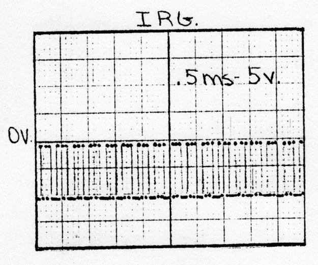
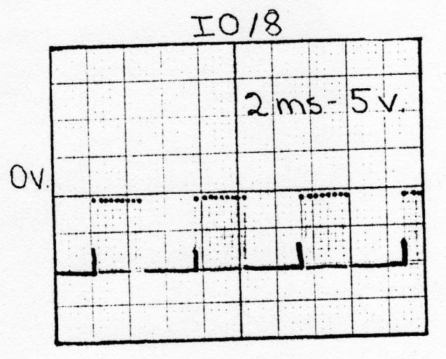
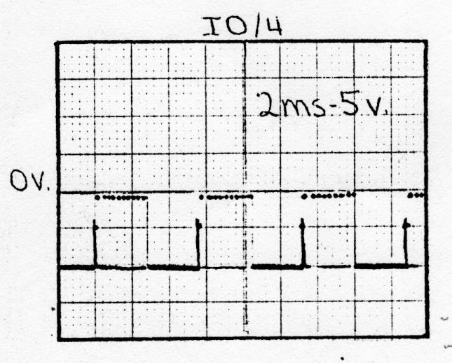
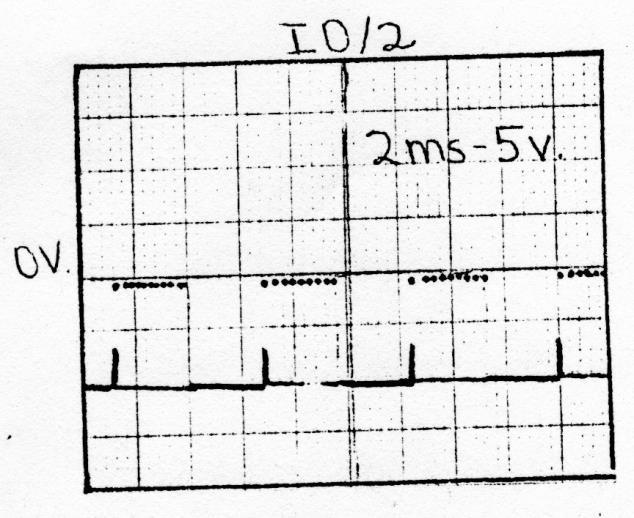
10 SR-52A MOS The MOS chip set consists of seven MOS devices. They are: 1) ARITHMETIC LOGIC CHIP (TMC501) 2) SCOM (TMC0534) - Scanning Read Only Memory 3) Two BROM's (TMC0562 & TMC0563) - Bare Read Only Memories 4) Two MULTI-REGISTER CHIPS (TMC0599) 5) MAG. I/O CHIP (TMC0595) 1) ARITHMETIC LOGIC CHIP (TMC0501E) The arithmetic logic chip, U1, performs the required mathematical operations using instructions from the SCOM and BROM's. The I/O, IRG, IDLE, and EXT lines are the communication links between the drivers. The arithmetic logic chip also receives instructions from the keyboard on its K lines and drives the display segments with the S (A-H) and DPT lines. 2) SCOM (TMC0534) The SCOM (U2) consists of a 13K word ROM used to store necessary functions used by the arithmetic logic chip. The SCOM also creates the display digit select signals (D-lines) and contains a special ROM which stores constants used in logarithmic and trigonometric functions. In addition to the above, the 534 also generates the 2 phase clock pulses that are necessary to drive the MOS chips. 3) BROMs (TMC0562, 0563) Each BROM (U3 & U4) provides a ROM extension of 1024 words for the SCOM, and uses the IRG, IDLE, and EXT lines to communicate with the SCOM and arithmetic logic chip. They also control motor turn on and turn off & also the power up clear. 4) MULTI-REGISTER CHIP (TMC0599) The multi-register chips (U5 & U6) provide program storage and user memory storage. Each chip has 30 storage registers capable of storing 1920 bits of data.
11 5) MAG I/O CHIP (TMC0595) The Mag I/O chip (U7) provides the interface between the four track magnetic card read/write mechanism and the arithmetic logic chip. Communications between the Mag I/O chip and arithmetic logic are carried on the IDLE, EXT, and IRG signal lines. The Mag I/O chip also conditions the signals to and from the magnetic card read/write mechanisms (e.g., motor, CSI, lamp, & CH1-4) to make them compatible with MOS logic levels.
12 KEYBOARD The keyboard is a simple switch matrix which connects a D-line signal from the SCOM chip to a K-Line input on the arithmetic logic chip when a key is pressed. Figure 2.4 shows the keyboard matrix with the approximate D and K-line connections for each valid instruction.

13 DISPLAY INTERFACE CIRCUIT The display is a fourteen digit, common cathode seven segment display. Each digit is driven by a D-line signal buffered by U8 or U9, and the segments are driven by the arithmetic logic chip such that the appropriate segments are turned on during each digit time. DISPLAY
14 MOTOR DRIVE CIRCUIT The motor drive circuit is a constant voltage circuit capable of driving the magnetic program card at a constant speed across the magnetic head (3.8 IPS nominal). When the calculator is instructed to read or write (keyboard entry) and the program card is slipped into the read/write mechanism, the card sense switch is opened and contact is broken between D-10 and U1 pin 10. When this occurs U7 pin 9 which is normally at VDD, switches to VSS. Resistors R7 and R9 constitutes a voltage divider which sets up the motor voltage. 1) As the value of R2 increases, the base of Q1 becomes more negative. Since Q1 is a PNP transistor, if the base of Q1 becomes more negative the collector becomes more positive. 2) If the base of Q2 becomes more positive, Q2 turns on harder trying to reach -VBatt. Result: Motor speed increases. 3) As the value of R2 decreases, the base of Q1 becomes more positive, the collector of Q1 becomes more negative. Since Q2 is a PNP transistor, Q2 is trying to turn off or trying to reach VSS. Result: Motor speed decreases. 4) As you increase R2, Q1 turns on, turning Q2 on, increasing motor speed. As you decrease R2, Q1 turns off, turning Q2 off, decreasing mo tor speed.
15 Motor Drive Circuit
16 CARD SENSOR INPUT SENSOR The card sensor input (CSI) circuit's purpose is to instruct the mag I/O interface chip (U7) that the program card is under the magnetic head (A1) and in the case of writing a program, that the correct card is being programmed (file protect). Under normal calculator operating conditions the motor is turned off and therefore, no current flows through the light emitting diode (LED) portion of SDA1 and no light is emitted. With no current flowing t hrough the sensor transistor of the SDA1, Q3 is turned on and U7 (pin 10) is held at VDD. When the calculator is instructed to read or write (keyboard entry) and the program card is slid into the calculator the motor turns on and current flows through the LED - R9 limits the current through the LED. Since the sensor uses reflected light, the current through the sensor transistor is still approximately zero (less than 1µA) until the leading edge of the program card passes under the sensor. When the program card is under the sensor the sensor transistor conducts current which turns off Q3, drawing U7 pin 10 to VSS. Because of sensitivity variations from one sensor to another, R5 is required to properly bias Q3 allowing the circuit to discriminate between a re flective portion of the program card and a non-reflective portion. R7 & the sensor transistor set up a variable current divider supplied by the current flowing through R5 to allow the necessary guard band between Q3 in saturation and in cut off. CR11 biase s Q3 by limiting the base current to no more than 2.5µA.
17 MAGNETIC READ/WRITE MECHANISM Information transfer between the calculator and the program card is accomplished by the magnetic read/write mechanism. The mechanism consists of a four track magnetic tape head, a normally closed switch and a card drive mechanism. The magnetic head is driven by four three-state buffers on U7 which allows the MOS to both read and write a magnetic card. The output of the magnetic head (each track) when reading is a series of pulses with alternating polarity approximately six to eight mv peak. The write signal out of the MOS is a square wave switching between approximately VSS and VDD. In both the read and write case, the frequency of the pulses/square wave varies depending upon the particular program (to include no signal on one or two tracks). The magnetic head is oriented such that track one is closest to the edge of the card. The magnetic read/write mechanism has a pressure pad which maintains contact between the magne tic head and the program card. Because the magnetic surface of the card must be in contact with the head throughout reading and writing, it is imperative that the pressure pad is functioning properly. The card speed is set at 3.8 inches per second (IPS). The calculator will function at a card speed of 3.3 IPS to 4.3 IPS. At any speed below 3.3 IPS, the magnetic head can generate the required output voltage to drive the TMS0595. At any speed above 4.3 IPS, the write length exceeds the length of the card. (It should be noted that the card speed increases during use.) A set up procedure for the card speed is given on the following page.
18 1) S e t mo t o r vo lt a g e t o vo lt a g e w r it t e n o n ma g ne t ic h e a d. 2) Wr it e o n a b la n k c a r d w it h a ll z e r o s ( e r a s e c a r d f ir s t ). 3) S p r a y c a r d w it h ma g ne t ic t a p e t r a c k de v e lo p e r ( ma g v ie w ). 4) M e a s u r e r e c o r d in g le n g t h - it s ho u ld be be t w e e n t o inc h e s. 5) I f o u t o f t h is r a ng e, a d ju s t R 7 a nd r e p e a t s t e p s 2 ), 3 ), & 4 ). 6) W h e n s p e e d is w it h in s p e c i f ic a t io n, c o r r e c t vo lt a g e w r it t e n o n t he ma g ne t ic he a d t o r e a d t he s e t vo lt a g e. 7) I nst a l l bo t t o m c a s e a nd r e p e a t s t e p s 2 ), 3 ), & 4 ). I f o u t o f s p e c i f ic a t io n r e t u r n t o s t e p 1) a nd s t a r t o ve r.
19 R E FE RE N CE C I R CU I T I n t he T M C I / O c h ip, t o r e ad a nd wr it e pro p e r ly, t he vo lt a g e U 7 p in 1 8 mu s t be ma int a ine d w it h in a t ig ht t o le r a nc e. T his is do ne by u s ing a r e fe r e nc e c ir c u it t o s et u p t he t hr e s ho ld vo lt a g e fo r t he s e nse a mp s in t he W he n t he vo lt ag e at U7 p in 1 1 is at V dd, Q5 is b ia s e d o ff a nd t he vo lt ag e at U 7 p in 1 8 f lo a t s at a p pro xima t e ly t he Z e n er vo lt a g e t o ma int a in a s ma ll c ha r g e o n t he fe e d ba c k c ap a c it o r s. ( C 9, C 1 0, C 11, C1 2) Whe n t he mo t o r is t ur ne d o n, t he vo lt a ge at U7 p in 1 1 s w it c he s fr o m V d d t o V s s. Qt s at ur at e s, a nd 2 0 ma f lo w s t hro u g h t he Z e ne r ( C R 1 7 ), s et t ing u p t he p r o p er r e fe r e nc e vo lt a g e at U 7 p in 1 8. T he r e fe r e nc e vo lt a ge, a nd t her e fo r e t he Z e ne r va lu e, d e p e nd u pon t he 59 5 r e v is io n. R e v is io n V R e f Z e ne r R 1 3 * T M C B 5. 1 ± 5% 1 N 7 51 A 240 T M C C 3. 3 ± 5% 1 N 7 56 A 330 T M C D - V bat t R e mo ve C R 1 7, Q 5, R13, R15, R19, a nd s ho r t - V B t o V bat t
20 SR-52A BLOCK DIAGRAM

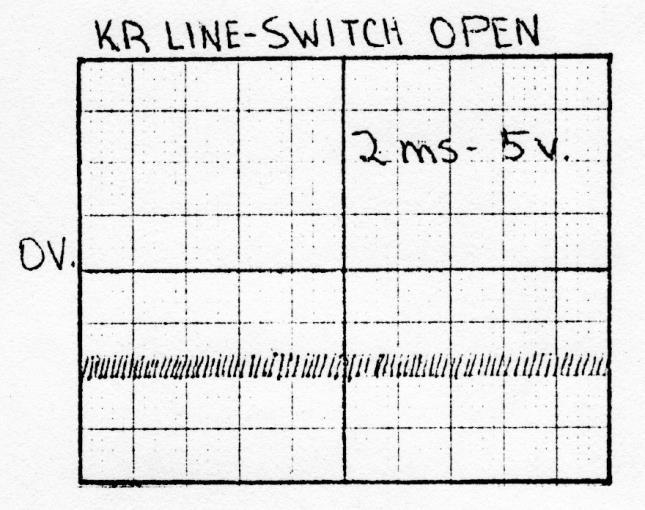
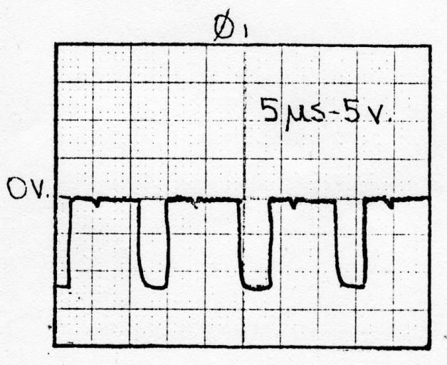
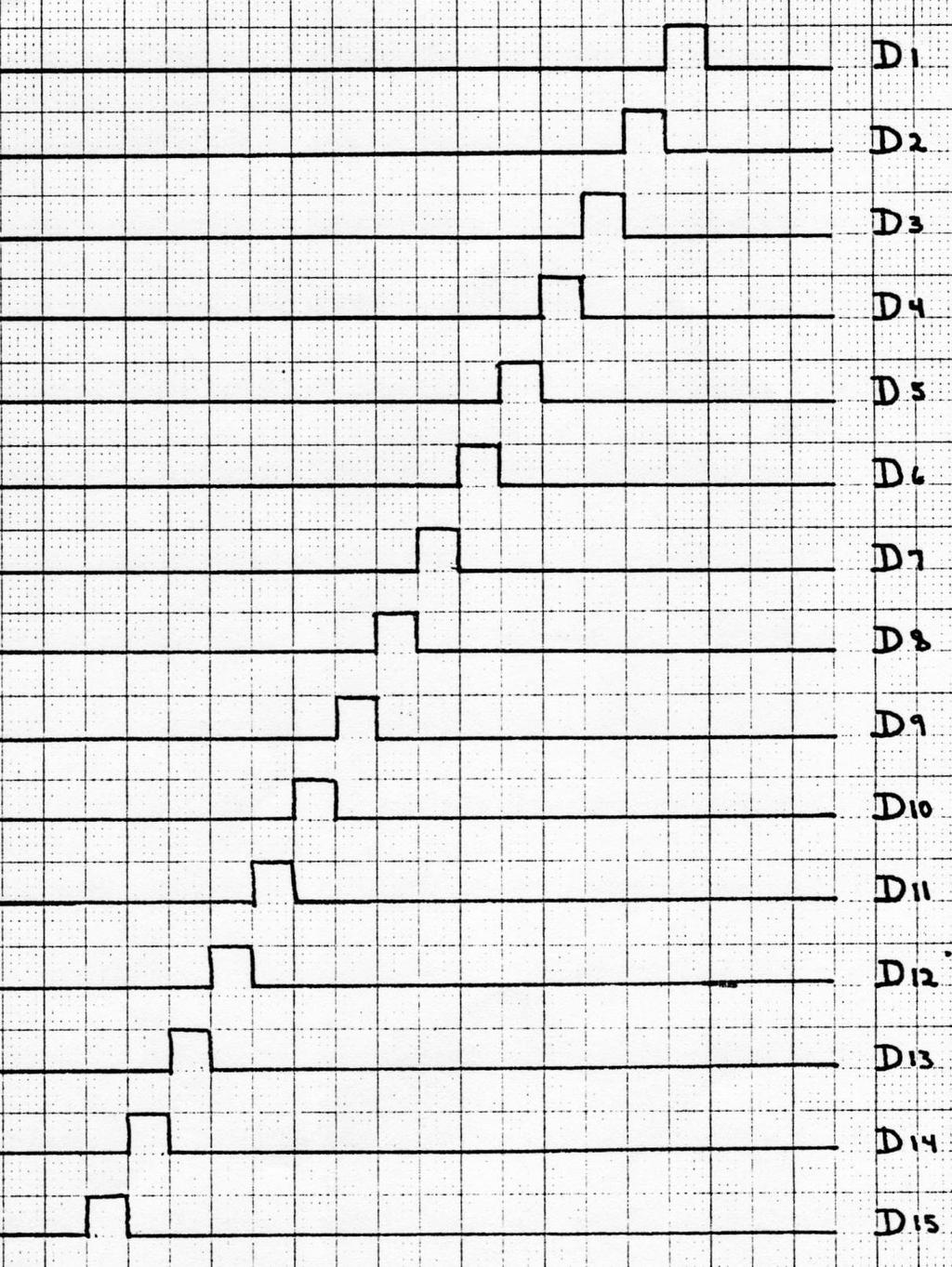
21 SR-52 WAVEFORMS DJD

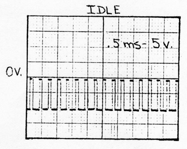
22 SR-52 WAVEFORMS DJD

23 SR-52 WAVEFORMS DJD
24

25 SR- 52 R e v. A t h r o u g h C - C O M P O N E N T L A Y O U T
26 SR- 52 R e v. D t h r o u g h J - C O M P O N E N T L A Y O U T
27 SR- 52 R e v. L - C O M P O N E N T L A Y O U T
28 SR- 52A C O M P O N E N T L A Y O U T
29 B I L L O F M A T E R I A L L I S T I N G 10/18/76 SD.DB107.LUB PAGE 1 Y330 LOWEST RUN AFFECTED: PROJ PARENT PART MC REV PART DESCRIPTION PART CYCLE ORD PLAN KIT WORK ORD WOMO DIST NUMBER LTR TYPE TIME POL OVG % DEL MADE ON BLOCK IDENT CODE SR-52 A WARRAN H LUB TY ***** ***** ************ ****** QTY PER ITM S PART NUMBER MC DESCRIPTION UM P CREDIT WOMO EQV TI PT NO DEL OPER EXT TOP CASE ASSY EA A $ RES 150 OHM EA P $ DIODE 1N757A EA P $ CAP 47UF EA P $ BATTERY CONTACT EA P $ MOS TMC501E EA P $ IC TMC0524 MOS EA P $ MOS TMC0562C EA P $ MOS TMC0563B EA P $ MOS TMC0595C EA P $ MOS TMC0599D EA P $ IC, SN27882 EA P $ IC SN97211 EA P $ IC 4011A EA P $ XSTR 2N3906 EA P $ XISTOR SKA1872 EA P $ XSTR, TIS92 EA P $
30 B I L L O F M A T E R I A L L I S T I N G 10/18/76 SD.DB107.LUB PAGE 2 Y330 LOWEST RUN AFFECTED: PROJ PARENT PART MC REV PART DESCRIPTION PART CYCLE ORD PLAN KIT WORK ORD WOMO DIST NUMBER LTR TYPE TIME POL OVG % DEL MADE ON BLOCK IDENT CODE SR-52 A WARRAN H LUB TY ***** ***** ************ ****** QTY PER ITM S PART NUMBER MC DESCRIPTION UM P CREDIT WOMO EQV TI PT NO DEL OPER EXT IDCTR TAP EA P $ RESONATOR EA P $ PCT 2.5MEG EA P $ POT 2.5K EA P $ XISTOR SKA3109 EA P $ XISTOR A5T4062 EA P $ VLED DISPLAY EA P $ ASSY KYBC SR52 EA P $ SWITCH EA P $ SWITCH DPST EA P $ ASSY SRCE-SENSR EA P $ RECEPTACLE EA P $ N746A DIODE EA P $ RES 180 OHM EA P $ RES 7.5K EA P $ IN751A 4000,410 EA P $ RES 4.7OHM 1 2K EA P $
31 B I L L O F M A T E R I A L L I S T I N G 10/18/76 SD.DB107.LUB PAGE 3 Y330 LOWEST RUN AFFECTED: PROJ PARENT PART MC REV PART DESCRIPTION PART CYCLE ORD PLAN KIT WORK ORD WOMO DIST NUMBER LTR TYPE TIME POL OVG % DEL MADE ON BLOCK IDENT CODE SR-52 A WARRAN H LUB TY ***** ***** ************ ****** QTY PER ITM S PART NUMBER MC DESCRIPTION UM P CREDIT WOMO EQV TI PT NO DEL OPER EXT HD MTG ASY EA P $ RES 1M EA P $ DECAL INSTR EA P $ RECEPTACLE EA P $ ADHESIVE EA P $ DR MOT/GEAR EA P $ EA P $ 41 LINES END OF REPORT < - - SUB-ITEM NOTES - - > TOTAL $4
32 B I L L O F M A T E R I A L L I S T I N G 10/18/76 SD.DB107.LUB PAGE 1 Y330 LOWEST RUN AFFECTED: PROJ PARENT PART MC REV PART DESCRIPTION PART CYCLE ORD PLAN KIT WORK ORD WOMO DIST NUMBER LTR TYPE TIME POL OVG % DEL MADE ON BLOCK IDENT CODE SR52A A WARRAN H LUB TY ***** ***** ************ ****** QTY PER ITM S PART NUMBER DESCRIPTION UM P CREDIT WOMO EQV TI PT NO DEL OPER EXT MC DIODE, RECT EA P $ DIODE, PG1992 EA P $ DIODE 1N754 EA P $ IN746A DIODE EA P $ CAP 47UF 6V EA P $ BATTERY CONTACT EA P $ MOS TMC501E EA P $ MOS TMC 534 EA P $ MOS TMC0562C EA P $ MOS TMC0563B EA P $ MOS TMC0595D EA P $ MOS TMC599D EA P $ IC, SN97311 EA P $ IC 4011A EA P $ XISTOR EA P $ XISTOR A5T3711 EA P $ XISTOR EA P $.01
33 B I L L O F M A T E R I A L L I S T I N G 10/18/76 SD.DB107.LUB PAGE 2 Y330 LOWEST RUN AFFECTED: PROJ PARENT PART MC REV PART DESCRIPTION PART CYCLE ORD PLAN KIT WORK ORD WOMO DIST NUMBER LTR TYPE TIME POL OVG % DEL MADE ON BLOCK IDENT CODE SR52A A WARRAN H LUB TY ***** ***** ************ ****** QTY PER ITM S PART NUMBER MC DESCRIPTION UM P CREDIT WOMO EQV TI PT NO DEL OPER EXT MODULE PS EA P $ RESONATOR EA P $ CAP, 22 UF EA P $ CAP, 47UF EA P $ CAP.005UF EA P $ PRINTER CONTACT EA P $ POT 2.5K EA P $ POT 2.5MEG EA P $ XSTR, TIS92 EA P $ CAP 47UF 6V EA P $ SR52 UPR HSC AS EA P $ RLB PRESS SR52 EA P $ CARD SPRING NEW EA P $ CONT MOT SWTCH EA P $ SCR EA P $ 33A SUB: EA P $ WIRE WHT 2 FT P $
34 B I L L O F M A T E R I A L L I S T I N G 10/18/76 SD.DB107.LUB PAGE 3 Y330 LOWEST RUN AFFECTED: PROJ PARENT PART MC REV PART DESCRIPTION PART CYCLE ORD PLAN KIT WORK ORD WOMO DIST NUMBER LTR TYPE TIME POL OVG % DEL MADE ON BLOCK IDENT CODE SR52A A WARRAN H LUB TY ***** ***** ************ ****** QTY PER ITM S PART NUMBER DESCRIPTION UM P CREDIT WOMO EQV TI PT NO DEL OPER EXT MC PAD RESILI EA P $ HD MTG ASY EA P $ SR52A LWRHSG EA P $ DR RLR SR52 EA P $ DR MOT/GEAR EA P $ ADHESIVE EA P $ INSERT SR52 EA P $ PRESSUR PAD EA P $ SCREW EA P $ SRCE-SESR ASY EA P $ VLED EA P $ SWITCH EA P $ SWITCH DPST EA P $ LEAD FR SR-50 A EA P $ INSULATOR EA P $ LEAD FRAME EA P $ TOP CASE ASY 52A EA P $.2
35 B I L L O F M A T E R I A L L I S T I N G 10/18/76 SD.DB107.LUB PAGE 4 Y330 LOWEST RUN AFFECTED: PROJ PARENT PART MC REV PART DESCRIPTION PART CYCLE ORD PLAN KIT WORK ORD WOMO DIST NUMBER LTR TYPE TIME POL OVG % DEL MADE ON BLOCK IDENT CODE SR52A A WARRAN H LUB TY ***** ***** ************ ****** QTY PER ITM S PART NUMBER MC DESCRIPTION UM P CREDIT WOMO EQV TI PT NO DEL OPER EXT KEYBOARD SUPT EA P $ WINDOW EA P $ SR52 BOT CASE EA P $ BLACK FEET EA P $ DECAL INSTR EA P $ 56 LINES END OF REPORT < - - SUB-ITEM NOTES - - > TOTAL $6
36 TI SR- 52A S C H E M A T I C D I A G R A M 1 OF 2
37 TI SR- 52A S C H E M A T I C D I A G R A M 2 OF 2
38 SR- 52 R EV. D T H R O U G H L - S C H E M A T I C D I A G R A M 1 OF 2
39 SR- 52 R EV. D T H R O U G H L - S C H E M A T I C D I A G R A M 2 OF 2

40 TI-22005
A L A BA M A L A W R E V IE W
 A L A BA M A L A W R E V IE W Volume 52 Fall 2000 Number 1 B E F O R E D I S A B I L I T Y C I V I L R I G HT S : C I V I L W A R P E N S I O N S A N D TH E P O L I T I C S O F D I S A B I L I T Y I N
T h e C S E T I P r o j e c t
 T h e P r o j e c t T H E P R O J E C T T A B L E O F C O N T E N T S A r t i c l e P a g e C o m p r e h e n s i v e A s s es s m e n t o f t h e U F O / E T I P h e n o m e n o n M a y 1 9 9 1 1 E T
P a g e 5 1 of R e p o r t P B 4 / 0 9
 P a g e 5 1 of R e p o r t P B 4 / 0 9 J A R T a l s o c o n c l u d e d t h a t a l t h o u g h t h e i n t e n t o f N e l s o n s r e h a b i l i t a t i o n p l a n i s t o e n h a n c e c o n n e
176 5 t h Fl oo r. 337 P o ly me r Ma te ri al s
 A g la di ou s F. L. 462 E l ec tr on ic D ev el op me nt A i ng er A.W.S. 371 C. A. M. A l ex an de r 236 A d mi ni st ra ti on R. H. (M rs ) A n dr ew s P. V. 326 O p ti ca l Tr an sm is si on A p ps
APPLICATION INSTRUC TIONS FOR THE
 APPLICATION INSTRUC TIONS FOR THE CHESS/ CHECKERBOARD Using the Che ss, Che c ke rs a nd Bo rd e rs: (SMALL), Pro duc t Numb e r: 11-1W-009 SIZE: a p p ro xima te ly 10 fe e t e a c h sid e ESTIMATED PAINT
CD4511BC BCD-to-7 Segment Latch/Decoder/Driver
 CD4511BC BCD-to-7 Segment Latch/Decoder/Driver General Description The CD4511BC BCD-to-seven segment latch/decoder/ driver is constructed with complementary MOS (CMOS) enhancement mode devices and NPN
PHOTO SCR OPTOCOUPLERS
 PACKAGE SCHEMATIC 6 6 ANODE 6 GATE CATHODE 2 5 ANODE N/C 3 4 CATHODE 6 DESCRIPTION The HC series consists of a gallium-arsenide infrared emitting diode optically coupled with a light activated silicon
MM74C912 6-Digit BCD Display Controller/Driver
 6-Digit BCD Display Controller/Driver General Description The display controllers are interface elements, with memory, that drive a 6-digit, 8-segment LED display. The display controllers receive data
3.3 V 256 K 16 CMOS SRAM
 August 2004 AS7C34098A 3.3 V 256 K 16 CMOS SRAM Features Pin compatible with AS7C34098 Industrial and commercial temperature Organization: 262,144 words 16 bits Center power and ground pins High speed
Beechwood Music Department Staff
 Beechwood Music Department Staff MRS SARAH KERSHAW - HEAD OF MUSIC S a ra h K e rs h a w t r a i n e d a t t h e R oy a l We ls h C o l le g e of M u s i c a n d D ra m a w h e re s h e ob t a i n e d
APPLICATION INSTRUCTIONS FOR THE
 APPLICATION INSTRUCTIONS FOR THE USA MA P WITH C A PITA LS & O C EA NS (LA RG E) Pro duc t Numbe r: 16-13W-051 SIZE: a ppro xima te ly 24 fe e t wide x 15 fe e t lo ng (ma inla nd o nly) ESTIMA TED PA
SPECIFICATION FOR LCD MODULE MODULE NO: AMC2004A-SPI REVISION NO: 00. Customer s Approval:
 SPECIFICATION FOR LCD MODULE MODULE NO: REVISION NO: 00 Customer s Approval: PREPARED BY (RD ENGINEER) CHECKED BY APPROVED BY SIGNATURE DATE DOCUMENT REVISION HISTORY: DATE PAGE DESCRIPTION 2013.2 - First
EMERGING DISPLAY CUSTOMER ACCEPTANCE SPECIFICATIONS 162A0(LED TYPES) EXAMINED BY : FILE NO. CAS ISSUE :NOV.18,1999 TOTAL PAGE : 8 APPROVED BY:
 EXAMINED BY : FILE NO. CAS ISSUE :NOV.18,1999 TOTAL PAGE : 8 APPROVED BY:") EXAMINED BY : FILE NO. CAS-10042 APPROVED BY: EMERGING DISPLAY TECHNOLOGIES CORPORATION ISSUE :NOV.18,1999 TOTAL PAGE : 8 VERSION : 3 CUSTOMER ACCEPTANCE SPECIFICATIONS MODEL : 162A0(LED TYPES) FOR MESSRS
EXAMINED BY : FILE NO. CAS-10042 APPROVED BY: EMERGING DISPLAY TECHNOLOGIES CORPORATION ISSUE :NOV.18,1999 TOTAL PAGE : 8 VERSION : 3 CUSTOMER ACCEPTANCE SPECIFICATIONS MODEL : 162A0(LED TYPES) FOR MESSRS
Grain Reserves, Volatility and the WTO
 Grain Reserves, Volatility and the WTO Sophia Murphy Institute for Agriculture and Trade Policy www.iatp.org Is v o la tility a b a d th in g? De pe n d s o n w h e re yo u s it (pro d uc e r, tra d e
c. What is the average rate of change of f on the interval [, ]? Answer: d. What is a local minimum value of f? Answer: 5 e. On what interval(s) is f
![c. What is the average rate of change of f on the interval [, ]? Answer: d. What is a local minimum value of f? Answer: 5 e. On what interval(s) is f](/thumbs/87/95703678.jpg "c. What is the average rate of change of f on the interval [, ]? Answer: d. What is a local minimum value of f? Answer: 5 e. On what interval(s) is f") Essential Skills Chapter f ( x + h) f ( x ). Simplifying the difference quotient Section. h f ( x + h) f ( x ) Example: For f ( x) = 4x 4 x, find and simplify completely. h Answer: 4 8x 4 h. Finding the
Essential Skills Chapter f ( x + h) f ( x ). Simplifying the difference quotient Section. h f ( x + h) f ( x ) Example: For f ( x) = 4x 4 x, find and simplify completely. h Answer: 4 8x 4 h. Finding the
DM74LS670 3-STATE 4-by-4 Register File
 DM74LS670 3-STATE 4-by-4 Register File General Description August 1986 Revised March 2000 These register files are organized as 4 words of 4 bits each, and separate on-chip decoding is provided for addressing
CRYSTAL CLEAR TECHNOLOGY SDN. BHD. Spec. No: CMC216-01
 LCD Module Specification 1.0 Table of Contents Page 1. Cover & Contents 1 2. Record of revision 2 3. General specification 3 4. Absolute maximum ratings 4 5. Electrical characteristics 4 6. Environmental
Table of C on t en t s Global Campus 21 in N umbe r s R e g ional Capac it y D e v e lopme nt in E-L e ar ning Structure a n d C o m p o n en ts R ea
 G Blended L ea r ni ng P r o g r a m R eg i o na l C a p a c i t y D ev elo p m ent i n E -L ea r ni ng H R K C r o s s o r d e r u c a t i o n a n d v e l o p m e n t C o p e r a t i o n 3 0 6 0 7 0 5
5 V 64K X 16 CMOS SRAM
 September 2006 A 5 V 64K X 16 CMOS SRAM AS7C1026C Features Industrial (-40 o to 85 o C) temperature Organization: 65,536 words 16 bits Center power and ground pins for low noise High speed - 15 ns address
Lesson Ten. What role does energy play in chemical reactions? Grade 8. Science. 90 minutes ENGLISH LANGUAGE ARTS
 Lesson Ten What role does energy play in chemical reactions? Science Asking Questions, Developing Models, Investigating, Analyzing Data and Obtaining, Evaluating, and Communicating Information ENGLISH
5.0 V 256 K 16 CMOS SRAM
 February 2006 5.0 V 256 K 16 CMOS SRAM Features Pin compatible with AS7C4098 Industrial and commercial temperature Organization: 262,144 words 16 bits Center power and ground pins High speed - 10/12/15/20
APPLICATION INSTRUCTIONS FOR THE
 APPLICATION INSTRUCTIONS FOR THE SNA KES A ND LA DDERS A DD O N FO R USE WITH THE C HESS, C HEC KERS & BO RDERS LARG E AND NUMBER SET Pro duc t Numb e r: 17-2W-062 SIZE: a ppro xima te ly 19 fe e t e a
P a g e 3 6 of R e p o r t P B 4 / 0 9
 P a g e 3 6 of R e p o r t P B 4 / 0 9 p r o t e c t h um a n h e a l t h a n d p r o p e r t y fr om t h e d a n g e rs i n h e r e n t i n m i n i n g o p e r a t i o n s s u c h a s a q u a r r y. J
Preliminary Datasheet
 Macroblock Preliminary Datasheet Features 3 output channels for RGB D lamps Output current invariant to load voltage change Programmable output current for each channel Built-in brightness control Constant
 Distributed by: www.jameco.com 1-800-831-4242 The content and copyrights of the attached material are the property of its owner. September 2001 S7C256 5V/3.3V 32K X 8 CMOS SRM (Common I/O) Features S7C256
HIGH SPEED-10 MBit/s LOGIC GATE OPTOCOUPLERS
 DESCRIPTION The / optocouplers consist of an AlGaAS LED, optically coupled to a very high speed integrated photo-detector logic gate with a strobable output. The devices are housed in a compact small-outline
Dangote Flour Mills Plc
 SUMMARY OF OFFER Opening Date 6 th September 27 Closing Date 27 th September 27 Shares on Offer 1.25bn Ord. Shares of 5k each Offer Price Offer Size Market Cap (Post Offer) Minimum Offer N15. per share
PHOTOTRANSISTOR OPTOCOUPLERS
 MCT MCTE MCT0 MCT7 MCT00 MCT0 MCT0 WHITE PACKAGE (-M SUFFIX) BLACK PACKAGE (NO -M SUFFIX) DESCRIPTION The MCTXXX series optoisolators consist of a gallium arsenide infrared emitting diode driving a silicon
PHOTODARLINGTON OPTOCOUPLERS
 DESCRIPTION The CNX48U, HBX, and TIL3 have a gallium arsenide infrared emitter optically coupled to a silicon planar photodarlington. CNX48U HB HB2 HB255 HB3 TIL3 FEATURES High sensitivity to low input
APPLICATION INSTRUC TIONS FOR THE
 APPLICATION INSTRUC TIONS FOR THE DAISY HOPSCOTCH Pro duc t Numb e r: 12-2W-03 SIZE: a p p ro xima te ly 14 fe e t hig h x 4 fe e t wid e. ESTIMATED PAINT TIME: a p p ro xima te ly 1 2 p e o p le fo r
3.3 V 64K X 16 CMOS SRAM
 September 2006 Advance Information AS7C31026C 3.3 V 64K X 16 CMOS SRAM Features Industrial (-40 o to 85 o C) temperature Organization: 65,536 words 16 bits Center power and ground pins for low noise High
Capacitor Discharge called CD welding
 TROUBLE SHOOTING OF STUD WELDING (EQUPMENT) We see several time, that the two main principles of Studwelding are mixed up therefor I will start to repeat short the welding methods. Capacitor Discharge
HARDENED PNP SILICON SWITCHING TRANSISTOR
 6 Lake Street, Lawrence, MA 01841 RADIATION HARDENED PNP SILICON SWITCHING TRANSISTOR Qualified per MIL-PRF-19500/291 DEVICES LEVELS 2N2906A 2N2907A JANSM 3K Rads (Si) 2N2906AL 2N2907AL JANSD 10K Rads
Use precise language and domain-specific vocabulary to inform about or explain the topic. CCSS.ELA-LITERACY.WHST D
 Lesson eight What are characteristics of chemical reactions? Science Constructing Explanations, Engaging in Argument and Obtaining, Evaluating, and Communicating Information ENGLISH LANGUAGE ARTS Reading
ARC 202L. Not e s : I n s t r u c t o r s : D e J a r n e t t, L i n, O r t e n b e r g, P a n g, P r i t c h a r d - S c h m i t z b e r g e r
 ARC 202L C A L I F O R N I A S T A T E P O L Y T E C H N I C U N I V E R S I T Y D E P A R T M E N T O F A R C H I T E C T U R E A R C 2 0 2 L - A R C H I T E C T U R A L S T U D I O W I N T E R Q U A
4-PIN PHOTOTRANSISTOR OPTOCOUPLERS
 PACKAGE HAA84 SCHEMATIC 4 COLLECTOR 4 2 3 EMITTER DESCRIPTION The HAA84 Series consists of two gallium arsenide infrared emitting diodes, connected in inverse parallel, driving a single silicon phototransistor
GENERAL PURPOSE 6-PIN PHOTOTRANSISTOR OPTOCOUPLERS
 4N37 HA HA2 HA3 HA4 HA5 WHITE PACKAGE (-M SUFFIX) SCHEMATIC 2 3 NC PIN. ANODE 2. CATHODE 3. NO CONNECTION 4. EMITTER 5. COLLECTOR. BASE 5 4 BLACK PACKAGE (NO -M SUFFIX) DESCRIPTION The general purpose
OH BOY! Story. N a r r a t iv e a n d o bj e c t s th ea t e r Fo r a l l a g e s, fr o m th e a ge of 9
 OH BOY! O h Boy!, was or igin a lly cr eat ed in F r en ch an d was a m a jor s u cc ess on t h e Fr en ch st a ge f or young au di enc es. It h a s b een s een by ap pr ox i ma t ely 175,000 sp ect at
Lecture 6 Power Zhuo Feng. Z. Feng MTU EE4800 CMOS Digital IC Design & Analysis 2010
 EE4800 CMOS Digital IC Design & Analysis Lecture 6 Power Zhuo Feng 6.1 Outline Power and Energy Dynamic Power Static Power 6.2 Power and Energy Power is drawn from a voltage source attached to the V DD
April 2004 AS7C3256A
 pril 2004 S7C3256 3.3V 32K X 8 CMOS SRM (Common I/O) Features Pin compatible with S7C3256 Industrial and commercial temperature options Organization: 32,768 words 8 bits High speed - 10/12/15/20 ns address
H11AV1-M H11AV1A-M H11AV2-M H11AV2A-M
 PACKAGE OUTLINE SCHEMATIC 6 6 HAVS-M, HAV2S-M 6 HAV-M, HAV2-M 2 3 NC PIN. ANODE 2. CATHODE 3. NO CONNECTION 4. EMITTER 5. COLLECTOR 6. BASE 5 4 6 HAVA-M, HAV2A-M DESCRIPTION The general purpose optocouplers
Diode. A diode is an semiconductor component that, in general, will pass current in only one direction
 Lecture 3 LED Diode A diode is an semiconductor component that, in general, will pass current in only one direction Water Analogy of Diodes Diode: How it Works Forward-biased ( open door ) Diode: How it
Executive Committee and Officers ( )
") Gifted and Talented International V o l u m e 2 4, N u m b e r 2, D e c e m b e r, 2 0 0 9. G i f t e d a n d T a l e n t e d I n t e r n a t i o n a2 l 4 ( 2), D e c e m b e r, 2 0 0 9. 1 T h e W o r
Gifted and Talented International V o l u m e 2 4, N u m b e r 2, D e c e m b e r, 2 0 0 9. G i f t e d a n d T a l e n t e d I n t e r n a t i o n a2 l 4 ( 2), D e c e m b e r, 2 0 0 9. 1 T h e W o r
SUNLIKE DISPLAY GENERAL SPECIFICATION
 GENERAL SPECIFICATION ITEM Product No SC0802EBLB-XA-GB-G DESCRIPTION STN Gray Positive STN Yellow Green Positive STN Blue Negative LCD Type TN Negative TN Positive FSTN Negative White & Black FSTN Positive
RADIATION HARDENED NPN SILICON SWITCHING TRANSISTOR Qualified per MIL-PRF-19500/255
 RADIATION HARDENED NPN SILICON SWITCHING TRANSISTOR Qualified per MIL-PRF-19500/255 DEVICES LEVELS 2N2221A 2N2222A JANSM 3K Rads (Si) 2N2221AL 2N2222AL JANSD K Rads (Si) 2N2221AUA 2N2222AUA JANSP 30K Rads
4-PIN PHOTOTRANSISTOR OPTOCOUPLERS
 PACKAGE HAA84 SCHEMATIC 4 COLLECTOR 4 2 3 EMITTER DESCRIPTION The HAA84 Series consists of two gallium arsenide infrared emitting diodes, connected in inverse parallel, driving a single silicon phototransistor
GENERAL PURPOSE 6-PIN PHOTOTRANSISTOR OPTOCOUPLERS
 TIL TIL-M TIL7-M MOC800-M WHITE PACKAGE (-M SUFFIX) SCHEMATIC 2 3 NC 5 4 PIN. ANODE 2. CATHODE 3. NO CONNECTION 4. EMITTER 5. COLLECTOR. BASE BLACK PACKAGE (NO -M SUFFIX) DESCRIPTION The MOC800, TIL and
MM74C912 6-Digit BCD Display Controller Driver MM74C917 6-Digit Hex Display Controller Driver
 MM74C912 6-Digit BCD Display Controller Driver MM74C917 6-Digit Hex Display Controller Driver General Description The MM74C912 MM74C917 display controllers are interface elements with memory that drive
S U E K E AY S S H A R O N T IM B E R W IN D M A R T Z -PA U L L IN. Carlisle Franklin Springboro. Clearcreek TWP. Middletown. Turtlecreek TWP.
 F R A N K L IN M A D IS O N S U E R O B E R T LE IC H T Y A LY C E C H A M B E R L A IN T W IN C R E E K M A R T Z -PA U L L IN C O R A O W E N M E A D O W L A R K W R E N N LA N T IS R E D R O B IN F
PS12038 Intellimod Module Application Specific IPM 25 Amperes/1200 Volts
 D M SQ PINS G L A F H K E J D VV QQ PP C 24 2 9 6 3 9 7 8 7 4 2 8 RR (4 PLACES) B N P Q R S Y EE XX V T LL DD GG TT SS X 2 3 4 GG T C FF LABEL T C 6 DD GG GG U P 2 N 3 NC 4 U V 6 W TERMINAL CODE 9 GND
N-Channel Enhancement-Mode Vertical DMOS FET
 N-Channel Enhancement-Mode Vertical DMOS FET Features Free from secondary breakdown Low power drive requirement Ease of paralleling Low C ISS and fast switching speeds Excellent thermal stability Integral
Description LB I/O15 I/O14 I/O13 I/O12 GND I/O11 I/O10 I/O9 I/O8
 18k x 16 HIGH SPEED ASYN CHRON OUS CMOS STATIC RAM Ex tended Tem per a ture TTS18WV16 FEATURES -High-speed access time: 0,5,35,45ns -Low Active Power: 55mW (typical) -Low stand-by power: 1 W (typical)
DM74S373 DM74S374 3-STATE Octal D-Type Transparent Latches and Edge-Triggered Flip-Flops
 3-STATE Octal D-Type Transparent Latches and Edge-Triggered Flip-Flops General Description These 8-bit registers feature totem-pole 3-STATE outputs designed specifically for driving highly-capacitive or
EE115C Digital Electronic Circuits Homework #4
 EE115 Digital Electronic ircuits Homework #4 Problem 1 Power Dissipation Solution Vdd =1.0V onsider the source follower circuit used to drive a load L =20fF shown above. M1 and M2 are both NMOS transistors
I N A C O M P L E X W O R L D
 IS L A M I C E C O N O M I C S I N A C O M P L E X W O R L D E x p l o r a t i o n s i n A g-b eanste d S i m u l a t i o n S a m i A l-s u w a i l e m 1 4 2 9 H 2 0 0 8 I s l a m i c D e v e l o p m e
 Distributed by: www.jameco.com 1-800-831-4242 The content and copyrights of the attached material are the property of its owner. DS0026 Dual High-Speed MOS Driver General Description DS0026 is a low cost
A new ThermicSol product
 A new ThermicSol product Double-Faced Thermo-Electric Solar-Panel TD/PV & Solar Tracker & Rotation Device An EU-patent protected product TP4-referens.pdf D o y o u w a n t to c o n v e rt it i n to G re
ATS177. General Description. Features. Applications. Ordering Information SINGLE OUTPUT HALL EFFECT LATCH ATS177 - P L - X - X
 Features General Description 3.5V to 20V DC operation voltage Temperature compensation Wide operating voltage range Open-Collector pre-driver 25mA maximum sinking output current Reverse polarity protection
CMSC 313 Lecture 17 Postulates & Theorems of Boolean Algebra Semiconductors CMOS Logic Gates
 CMSC 313 Lecture 17 Postulates & Theorems of Boolean Algebra Semiconductors CMOS Logic Gates UMBC, CMSC313, Richard Chang Last Time Overview of second half of this course Logic gates &
INSTRUCTIONS: CHEM Exam I. September 13, 1994 Lab Section
 CHEM 1314.05 Exam I John I. Gelder September 13, 1994 Name TA's Name Lab Section Please sign your name below to give permission to post, by the last 4 digits of your student I.D. number, your course scores
Results as of 30 September 2018
 rt Results as of 30 September 2018 F r e e t r a n s l a t ion f r o m t h e o r ig ina l in S p a n is h. I n t h e e v e n t o f d i s c r e p a n c y, t h e Sp a n i s h - la n g u a g e v e r s ion
8. Relax and do well.
 CHEM 1314.03 Exam I John I. Gelder September 25, 1997 Name TA's Name Lab Section Please sign your name below to give permission to post, by the last 4 digits of your student I.D. number, your course scores
DS1225Y. 64K Nonvolatile SRAM FEATURES PIN ASSIGNMENT
 DS1225Y 64K Nonvolatile SRAM FEATURES years minimum data retention in the absence of external power PIN ASSIGNMENT NC 1 28 VCC Data is automatically protected during power loss Directly replaces 8K x 8
Lecture 21: Packaging, Power, & Clock
 Lecture 21: Packaging, Power, & Clock Outline Packaging Power Distribution Clock Distribution 2 Packages Package functions Electrical connection of signals and power from chip to board Little delay or
VLSI GATE LEVEL DESIGN UNIT - III P.VIDYA SAGAR ( ASSOCIATE PROFESSOR) Department of Electronics and Communication Engineering, VBIT
 Department of Electronics and Communication Engineering, VBIT") VLSI UNIT - III GATE LEVEL DESIGN P.VIDYA SAGAR ( ASSOCIATE PROFESSOR) contents GATE LEVEL DESIGN : Logic Gates and Other complex gates, Switch logic, Alternate gate circuits, Time Delays, Driving large
VLSI UNIT - III GATE LEVEL DESIGN P.VIDYA SAGAR ( ASSOCIATE PROFESSOR) contents GATE LEVEL DESIGN : Logic Gates and Other complex gates, Switch logic, Alternate gate circuits, Time Delays, Driving large
Last 4 Digits of USC ID:
 Chemistry 05 B Practice Exam Dr. Jessica Parr First Letter of last Name PLEASE PRINT YOUR NAME IN BLOCK LETTERS Name: Last 4 Digits of USC ID: Lab TA s Name: Question Points Score Grader 8 2 4 3 9 4 0
T C MEASURED POINT G1 E1 E2 G2 W - (4 PLACES) G2 E2 E1 G1
 G2 E2 E1 G1") CMDU-3KA Powerex, Inc., Hillis Street, Youngwood, Pennsylvania 15697-1 (7) 95-77 Dual IGBTMOD KA-Series Module Amperes/17 Volts B F A G T C MEASURED POINT M C L T - ( TYP.) N R Z CE1 E C1 C E AA S - (3
CMDU-3KA Powerex, Inc., Hillis Street, Youngwood, Pennsylvania 15697-1 (7) 95-77 Dual IGBTMOD KA-Series Module Amperes/17 Volts B F A G T C MEASURED POINT M C L T - ( TYP.) N R Z CE1 E C1 C E AA S - (3
MOC8111 MOC8112 MOC8113
 PACKAGE SCHEMATIC ANODE 6 N/C 6 6 CATHODE 2 5 COLLECTOR N/C 3 4 EMITTER 6 DESCRIPTION The MOC8X series consists of a Gallium Arsenide IRED coupled with an NPN phototransistor. The base of the transistor
TEPZZ A T EP A2 (19) (11) EP A2 (12) EUROPEAN PATENT APPLICATION. (51) Int Cl.: H02M 7/483 ( )
 (11) EP A2 (12) EUROPEAN PATENT APPLICATION. (51) Int Cl.: H02M 7/483 ( )") (19) TEPZZ 7849 6A T (11) EP 2 784 926 A2 (12) EUROPEAN PATENT APPLICATION (43) Date of publication: 01..14 Bulletin 14/40 (1) Int Cl.: H02M 7/483 (07.01) (21) Application number: 14162389.2 (22) Date
(19) TEPZZ 7849 6A T (11) EP 2 784 926 A2 (12) EUROPEAN PATENT APPLICATION (43) Date of publication: 01..14 Bulletin 14/40 (1) Int Cl.: H02M 7/483 (07.01) (21) Application number: 14162389.2 (22) Date
Homework assignment from , MEMS Capacitors lecture
 Homework assignment from 05-02-2006, MEMS Capacitors lecture 1. Calculate the capacitance for a round plate of 100µm diameter with an air gap space of 2.0 µm. C = e r e 0 * A/d (1) e 0 = 8.85E-12 F/m e
CD4514BC CD4515BC 4-Bit Latched/4-to-16 Line Decoders
 CD4514BC CD4515BC 4-Bit Latched/4-to-16 Line Decoders General Description The CD4514BC and CD4515BC are 4-to-16 line decoders with latched inputs implemented with complementary MOS (CMOS) circuits constructed
Solutions and Ions. Pure Substances
 Class #4 Solutions and Ions CHEM 107 L.S. Brown Texas A&M University Pure Substances Pure substance: described completely by a single chemical formula Fixed composition 1 Mixtures Combination of 2 or more
II/IV B.Tech. DEGREE EXAMINATIONS, NOV/DEC-2017
 CSE/IT 213 (CR) Total No. of Questions :09] [Total No. of Pages : 03 II/IV B.Tech. DEGREE EXAMINATIONS, NOV/DEC-2017 First Semester CSE/IT BASIC ELECTRICAL AND ELECTRONICS ENGINEERING Time: Three Hours
Circle the letters only. NO ANSWERS in the Columns!
 Chemistry 1304.001 Name (please print) Exam 5 (100 points) April 18, 2018 On my honor, I have neither given nor received unauthorized aid on this exam. Signed Date Circle the letters only. NO ANSWERS in
NTE74HC299 Integrated Circuit TTL High Speed CMOS, 8 Bit Universal Shift Register with 3 State Output
 NTE74HC299 Integrated Circuit TTL High Speed CMOS, 8 Bit Universal Shift Register with 3 State Output Description: The NTE74HC299 is an 8 bit shift/storage register with three state bus interface capability
Designing a Thermostat Worksheet
 Designing a Thermostat Worksheet Most of us have a thermostat in our homes to control heating and cooling systems of our home. These important devices help us save energy by automatically turning off energy
Digital Electronics Circuits 2017
 JSS SCIENCE AND TECHNOLOGY UNIVERSITY Digital Electronics Circuits (EC37L) Lab in-charge: Dr. Shankraiah Course outcomes: After the completion of laboratory the student will be able to, 1. Simplify, design
AZ DISPLAYS, INC. COMPLETE LCD SOLUTIONS SPECIFICATIONS FOR LIQUID CRYSTAL DISPLAY
 COMPLETE LCD SOLUTIONS SPECIFICATIONS FOR LIQUID CRYSTAL DISPLAY PART NUMBER: DATE: APRIL 01, 2008 General Specification Driving IC NT7534 Interace With Paraller MPU 8080 Series Display Specification Display
PI4GTL bit bidirectional low voltage translator
 Features 2-bit bidirectional translator Less than 1.5 ns maximum propagation delay to accommodate Standard mode and Fast mode I2Cbus devices and multiple masters Allows voltage level translation between
NTE4035B Integrated Circuit CMOS, 4 Bit Parallel In/Parallel Out Shift Register
 NTE4035B Integrated Circuit CMOS, 4 Bit Parallel In/Parallel Out Shift Register Description: The NTE4035B is a 4 bit shift register in a 16 Lead DIP type package constructed with MOS P Channel an N Channel
PNP SILICON SWITCHING TRANSISTOR Qualified per MIL-PRF-19500/357
 DEVICES PNP SILICON SITCHING TRANSISTOR Qualified per MIL-PRF-19500/357 LEVELS 2N3634 2N3635 2N3636 2N3637 JAN 2N3634L 2N3635L 2N3636L 2N3637L JANTX 2N3634UB 2N3635UB 2N3636UB 2N3637UB JANTXV JANS ABSOLUTE
CD4013BC Dual D-Type Flip-Flop
 Dual D-Type Flip-Flop General Description The CD4013B dual D-type flip-flop is a monolithic complementary MOS (CMOS) integrated circuit constructed with N- and P-channel enhancement mode transistors. Each
PHOTOTRANSISTOR OPTOCOUPLERS
 DESCRIPTION The CNY7 series consists of a Gallium Arsenide IRED coupled with an NPN phototransistor. FEATURES CNY7-/2/3 are also available in white package by specifying -M suffix (eg. CNY7-2-M) UL recognized
70 mv typ. (2.8 V output product, I OUT = 100 ma)
") S-1335 Series www.ablicinc.com HIGH RIPPLE-REJECTION SOFT-START FUNCTION CMOS VOLTAGE REGULATOR ABLIC Inc., 212-214 Rev.1.3_2 The S-1335 Series, developed by using the CMOS technology, is a positive voltage
S-1335 Series www.ablicinc.com HIGH RIPPLE-REJECTION SOFT-START FUNCTION CMOS VOLTAGE REGULATOR ABLIC Inc., 212-214 Rev.1.3_2 The S-1335 Series, developed by using the CMOS technology, is a positive voltage
74LCX16374 Low Voltage 16-Bit D-Type Flip-Flop with 5V Tolerant Inputs and Outputs
 74LCX16374 Low oltage 16-Bit D-Type Flip-Flop with 5 Tolerant Inputs and Outputs General Description The LCX16374 contains sixteen non-inverting D-type flip-flops with 3-STATE outputs and is intended for
Software Process Models there are many process model s in th e li t e ra t u re, s om e a r e prescriptions and some are descriptions you need to mode
 Unit 2 : Software Process O b j ec t i ve This unit introduces software systems engineering through a discussion of software processes and their principal characteristics. In order to achieve the desireable
AK AJ AT AR DETAIL "A" N M L K B AB (6 PLACES) DETAIL "B" TH1 (11) TH2 (10) NTC *ALL PIN DIMENSIONS WITHIN A TOLERANCE OF ±0.5
 DETAIL B TH1 (11) TH2 (10) NTC *ALL PIN DIMENSIONS WITHIN A TOLERANCE OF ±0.5") Powerex, Inc., 73 Pavilion Lane, Youngwood, Pennsylvania 5697 (724) 925-7272 www.pwrx.com Six IGBTMOD + Brake NX-S Series Module AH AN AC AD AE H AK AJ A D E F G AK AJ AP AT AR AQ AS C AX BB BC BD DETAIL
Powerex, Inc., 73 Pavilion Lane, Youngwood, Pennsylvania 5697 (724) 925-7272 www.pwrx.com Six IGBTMOD + Brake NX-S Series Module AH AN AC AD AE H AK AJ A D E F G AK AJ AP AT AR AQ AS C AX BB BC BD DETAIL
SPECIFICATION FOR LCD MODULE MODULE NO: AMC0802B-I2C REVISION NO: 00
 SPECIFICATION FOR LCD MODULE MODULE NO: REVISION NO: 00 Customer s Approval: PREPARED BY (RD ENGINEER) CHECKED BY APPROVED BY SIGNATURE DATE 14925 SE Allen Road, Suite 203B, Bellevue, WA 98006 Tel: 425-698-1938
MOC205-M MOC206-M MOC207-M MOC208-M
 DESCRIPTION These devices consist of a gallium arsenide infrared emitting diode optically coupled to a monolithic silicon phototransistor detector, in a surface mountable, small outline, plastic package.
NTE74LS181 Integrated Circuit TTL Arithmetic Logic Unit/Function Generator
 NTE74LS181 Integrated Circuit TTL Arithmetic Logic Unit/Function Generator Description: The NTE74LS181 is an arithmetic logic unit (ALU)/function generator in a 24 Lead DIP type package that has the complexity
INTERIM MANAGEMENT REPORT FIRST HALF OF 2018
 INTERIM MANAGEMENT REPORT FIRST HALF OF 2018 F r e e t r a n s l a t ion f r o m t h e o r ig ina l in S p a n is h. I n t h e e v e n t o f d i s c r e p a n c y, t h e Sp a n i s h - la n g u a g e v
Chemistry 2 Exam Roane State Academic Festival. Name (print neatly) School
 School") Name (print neatly) School There are fifteen question on this exam. Each question is weighted equally. n the answer sheet, write your name in the space provided and your answers in the blanks provided.
Name (print neatly) School There are fifteen question on this exam. Each question is weighted equally. n the answer sheet, write your name in the space provided and your answers in the blanks provided.
Alles Taylor & Duke, LLC Bob Wright, PE RECORD DRAWINGS. CPOW Mini-Ed Conf er ence Mar ch 27, 2015
 RECORD DRAWINGS CPOW Mini-Ed Conf er ence Mar ch 27, 2015 NOMENCLATURE: Record Draw ings?????? What Hap p ened t o As- Built s?? PURPOSE: Fur n ish a Reco r d o f Co m p o n en t s Allo w Locat io n o
IRGPC40UD2 UltraFast CoPack IGBT
 INSULATED GATE BIPOLAR TRANSISTOR WITH ULTRAFAST SOFT REOVERY DIODE PD - 9.88A UltraFast opack IGBT Features Switching-loss rating includes all "tail" losses HEXFRED TM soft ultrafast diodes Optimized
F48T10VHO, F60T10VHO, F72T10VHO, F96T12HO (1 LAMP ONLY) ELECTRICAL DATA (120V APPLICATION)
 ELECTRICAL DATA (120V APPLICATION)") LOW TEMPERATURE ELECTRONIC F72T8HO (1 ONLY) (1 ONLY) ELECTRICAL DATA (120V APPLICATION) /(N) /(L) INPUT VOLT: 120V ± 10%, 50/60Hz WATTS/TYPE F48T8HO F60T8HO F72T8HO F48T12HO F60T12HO F72T12HO F96T12HO
LOW TEMPERATURE ELECTRONIC F72T8HO (1 ONLY) (1 ONLY) ELECTRICAL DATA (120V APPLICATION) /(N) /(L) INPUT VOLT: 120V ± 10%, 50/60Hz WATTS/TYPE F48T8HO F60T8HO F72T8HO F48T12HO F60T12HO F72T12HO F96T12HO
NAME SID EE42/100 Spring 2013 Final Exam 1
 NAME SID EE42/100 Spring 2013 Final Exam 1 1. Short answer questions a. There are approximately 36x10 50 nucleons (protons and neutrons) in the earth. If we wanted to give each one a unique n-bit address,
P4C164 ULTRA HIGH SPEED 8K X 8 STATIC CMOS RAMS FEATURES DESCRIPTION. Full CMOS, 6T Cell. Common Data I/O
 FEATURES Full CMOS, 6T Cell High Speed (Equal Access and Cycle Times) 8/10/12/15/20/25/35/70/100 ns (Commercial) 10/12/15/20/25/35/70/100 ns(industrial) 12/15/20/25/35/45/70/100 ns (Military) Low Power
HIGH SPEED TRANSISTOR OPTOCOUPLERS
 SINGLECHANNEL: PACKAGE SCHEMATIC N/C V CC + V CC V F + V F 7 V B _ 7 V 0 _ V O _ V 0 V F N/C 4 5 GND + 4 5 GND,,, Pin 7 is not connected in Part Number / DESCRIPTION The /, / and / optocouplers consist
Use precise language and domain-specific vocabulary to inform about or explain the topic. CCSS.ELA-LITERACY.WHST D
 Lesson seven What is a chemical reaction? Science Constructing Explanations, Engaging in Argument and Obtaining, Evaluating, and Communicating Information ENGLISH LANGUAGE ARTS Reading Informational Text,
CHEM 10113, Quiz 5 October 26, 2011
 CHEM 10113, Quiz 5 October 26, 2011 Name (please print) All equations must be balanced and show phases for full credit. Significant figures count, show charges as appropriate, and please box your answers!