Designing Sequential Logic Circuits
|
|
|
- Erin Mitchell
- 5 years ago
- Views:
Transcription

1 igital Integrated Circuits (83-313) Lecture 5: esigning Sequential Logic Circuits Semester B, Lecturer: r. Adam Teman TAs: Itamar Levi, Robert Giterman 26 April 2017 isclaimer: This course was prepared, in its entirety, by Adam Teman. Many materials were copied from sources freely available on the internet. When possible, these sources have been cited; however, some references may have been cited incorrectly or overlooked. If you feel that a picture, graph, or code example has been copied from you and either needs to be cited or removed, please feel free to adam.teman@biu.ac.il and I will address this as soon as possible.


2 Sequential Logic Sequential circuits are a function of both the current state and the previous state. In other words, they have memory. The majority of sequential circuits are Synchronous, using a clock to synchronize the logic paths. 2
3 3 Lecture Content

4 4 Why use Sequential Logic?
5 Explanation through example We will look at two examples: An accumulator circuit, where sequential methods are essential to eliminate races. A pipelined system, where sequential methods improve throughput. 5


6 6 What would happen if there were no traffic lights?
7 Accumulator Example An accumulator is a register that sums a list of numbers. Therefore, it feeds back the output back to the input. Without a register, there would be the possibility that the input would change before the calculation was finished. We need to delay the output until the original calculation is finished. IN =11 1+1=0 c1 + XX c10 OUT X00 c
8 Accumulator Example It is essential to use sequential logic when paths have different delays, but need to converge together. We always have to slow our fast paths down so they arrive along with our slowest path. If we could make all paths have equal delays, we wouldn t need sequential logic, but this is really hard (almost impossible) to do. 8
9 Laundry Example Small laundry has one washer, one dryer and one operator, it takes 90 minutes to finish one load: Washer takes 30 minutes ryer takes 40 minutes operator folding takes 20 minutes 9


10 Sequential Laundry It takes 90 minutes to finish one load. The process is sequential. Sequential laundry takes 6 hours for 4 loads. 10

11 Pipelined Laundry Every 40 minutes a new load starts and a new load ends. Pipelined laundry takes 3.5 hours for 4 loads 11
12 Instruction Output Pipelining ata If it takes 10 time units to process an instruction, we could perform one instruction every 10 time units: Instruction Output elay But if we divide the process into 5 tasks that take 2 time units each: 12 elay We can start a new instruction every 2 time units. And after filling the pipe, we finish an instruction every 2 units.
13 Pipelining ata But some stages may be faster than others, so we need to hold the input to each stage constant until the previous stage is done. We achieve this by adding a register in between the stages. So by using a pipeline, we can make our slowest path shorter and therefore reduce the delay between actions. All data paths are built using a pipeline of some sort, either to eliminate races or to increase throughput. 13


14 MIPS Pipeline source: wikipedia 14
15 15 Sequential Logic Elements
16 sample sample Naming Conventions In our course we relate to registers as follows: a latch is level sensitive transparent transparent opaque opaque a flip-flop is edge-triggered locked locked 16 There are many different naming conventions For instance, many books call any bi-stable element a flip-flop (such as an SR Latch) However, this leads to confusion, so we will use the convention above (as used in industry).
17 Latch Vs. Register uring high clock phases, a latch is transparent, latching the input on the falling edge. However, a Flip Flop only samples the input on the rising edge. Clock Input () Latch Q 17 Flip Flop Q


18 Latch Vs. Register 3 main options for sequential timing: Using Flip-Flops Using Transparent Latches Using Pulsed Latches 18
19 Static Vs. ynamic Latch A static latch stores its output in a static state A dynamic latch uses temporary capacitance to store its state. As with logic, this provides a trade-off between area, speed and reliability. S 0 CLK Q MUX 2:1 Q S 1 S 19 CLK Static Latch ynamic Latch
20 Static Vs. ynamic Latch Some basic implementations of static and dynamic latches. Static CLK CLK ynamic Q CLK Q CLK CLK 20
21 Ratioed vs. Non-Ratioed Latch A static latch can be made by using a feedback inverter. The TG (with the driver before it) must overcome the feedback inverter to write into the latch. CLK CLK But it is usually more robust to create a mux-based non-ratioed latch. At the expense of size. CLK CLK Q 21 CLK
22 mid Making a Flip Flop Input Q Q out Conceptually, we can create an edge triggered flip-flop by combining two opposite polarity latches: clk clk Input Q mid Q out 22
23 Master-Slave (Edge-Triggered) Register Two opposite latches trigger on edge Also called master-slave latch pair 23
24 Master-Slave Register Multiplexer-based latch pair I 2 T 2 I 3 I 5 T 4 I 6 Q I 1 T 1 Q M I 4 T 3 CLK 24 How many transistors make up this flip-flop? What is its clock load?


25 Resettable Flip Flops Asynchronous Set/Reset Flip-Flop Synchronous Reset Flip-Flop 25
26 26 Timing Parameters of Sequential Elements
27 Timing efinitions Register Q CLK CLK t t setup ATA STABLE t hold t cq t t cq t setup propagation delay setup time Q ATA STABLE t t hold hold time 27

28 Clk-Q elay - t cq t cq is the time from the clock edge until the data appears at the output. The t cq for rising and falling outputs is different. clk Q t cqlh t cqhl t cqlh 28
29 Mux based FF t cq Calculation uring low clock edge, data traverses slave and waits for the clock at pass gate input. When clock rises, data has to go through pass gate and inverter. I 2 T 2 I 3 I 5 T 4 I 6 Q I 1 T 1 Q M I 4 T 3 CLK t T I cq
30 Timing efinitions Register Q CLK CLK t t setup ATA STABLE t hold t cq t t cq t setup propagation delay setup time Q ATA STABLE t t hold hold time 30
31 Setup Time - t su Setup time is the time the data has to arrive before the clock to ensure correct sampling. clk t su t su t su Good! Good! BA! Q 31
32 Mux based FF t su Calculation Before clock edge, data should have propagated to the latching pass gate, or else data will be restored to the previous state. I 2 T 2 I 3 I 5 T 4 I 6 Q I 1 T 1 Q M I 4 T 3 CLK 32 t I T I I T I su

33 Timing Analysis - Setup Time To obtain the setup time of the register while using SPICE, we progressively skew the input with respect to the clock edge until the circuit fails. 33
34 Timing efinitions Register Q CLK CLK t t setup ATA STABLE t hold t cq t t cq t setup propagation delay setup time Q ATA STABLE t t hold hold time 34


35 Hold Time - t hold Hold time is the time the data has to be stable after the clock to ensure correct sampling. clk t hold t hold t hold Good! Good! BA! Q Often (optimally), Hold Time is negative! 35
36 Mux based FF t hold Calculation When the clock rises, T 1 closes, latching the data at the output of I 1. Therefore, any changes made t pd (I 1 ) before the clock will not traverse. The hold time is t pd (I 1 ) I 2 T 2 I 3 I 5 T 4 I 6 Q CLK I 1 T 1 Q M I 4 T 3 thold I 1 36
37 Characterizing Timing t - Q Q Q Clk Clk t C - Q t C - Q Register Latch 37
38 38 Other Flip Flop Implementations
39 Problem Clock Overlap CLK CLKb I 2 T 2 I 3 I 5 T 4 I 6 Q I 1 T 1 Q M I 4 T 3 CLK 39


40 C 2 MOS clocked CMOS Insensitive to clock overlap. Low Phase Overlap High Phase Overlap CLK 40 CLKb


")
41 TSPC True Single-Phase Clocked Register TSPC enables including logic inside the latch! Positive latch (transparent when CLK= 1) Example: AN latch 41 Negative latch (transparent when CLK= 0)
42 TSPC Flip Flop V V V M 3 CLK M 6 M 9 Q Y Q CLK M 2 X M 5 CLK M 8 M 1 CLK M 4 M 7 42

43 Pulse-Triggered Latches Instead of a full set of master-slave latches We can emulate an edge with a short clock pulse: ata Clk Master-Slave Latches L1 L2 Q Q Clk Clk ata Pulse-Triggered Latch L Q esign a clock pulse with a clock chopper Clk Clk 43
44 44 Basic Timing Constraints
45 45 Synchronous Timing
46 Timing Constraints There are two main problems that can arise in synchronous logic: Max elay: The data doesn t have enough time to pass from one register to the next before the next clock edge. Min elay: The data path is so short that it passes through several registers during the same clock cycle. Max delay violations are a result of a slow data path, including the registers t setup, therefore it is often called the Setup path. Min delay violations are a result of a short data path, causing the data to change before the t hold has passed, therefore it is often called the Hold path. 46
47 Setup (Max) Constraint Let s see what makes up our clock cycle: After the clock rises, it takes t cq for the data to propagate to point A. Then the data goes through the delay of the logic to get to point B. The data has to arrive at point B, t setup before the next clock. In general, our timing path is a race: Between the ata Arrival, starting with the launching clock edge. And the ata Capture, one clock period later. clk t cq Q Q A Logic B 47 A B t su clk
48 Setup (Max) Constraint T t t t cq logic setup 48
49 Hold (Min) Constraint Hold problems occur due to the logic changing before t hold has passed. This is not a function of cycle time it is relative to a single clock edge! Let s see how this can happen: The clock rises and the data at A changes after t cq. The data at B changes t pd (logic) later. Since the data at B had to stay stable for t hold after the clock (for the second register), the change at B has to be at least t hold after the clock edge. 49 clk A B t cq t hold Logic Q Q clk A B
50 Hold (Min) Constraint t t t cq logic hold 50
51 Summary For Setup constraints, the clock period has to be longer than the data path delay: This sets our maximum frequency. If we have setup failures, we can always just slow down the clock. T t t t cq logic setup For Hold constrains, the data path delay has to be longer than the hold time: This is independent of clock period. If there is a hold failure, you can throw your chip away! t t t cq logic hold 51
52 t RV_CLK Clock Nonidealities Ref_Clock Clock skew t skew t jit t skew t jit Spatial variation in temporally equivalent clock edges; deterministic + random, t skew t RVCLK Received Clock trcv_clk T Clock uncertainty: jitter+skew Clock jitter Temporal variations in consecutive edges of the clock signal; modulation + random noise Cycle-to-cycle (short-term) t Jit,S Long term t Jit,L Ref_Clock t skew t jit t skew t jit 52 Variation of the pulse width Important for level sensitive clocking Received Clock t RCVCLK T
53 Positive and Negative Skew In R1 Q Combinational Logic R2 Q Combinational Logic R3 Q CLK t CLK1 t CLK2 t CLK3 delay Positive skew delay In R1 Q Combinational Logic R2 Q Combinational Logic R3 Q t CLK1 t CLK2 t CLK3 delay Negative skew delay CLK 53
54 Setup (Max) Constraint The Launch path (still) consists of: 54 t cq +t logic +t setup But if jitter makes the launch clock later, we need to add it to the data path delay. The Capture path consists of: The clock period (T) Positive skew means the capture clock path is longer. t T t If jitter makes the capture clock earlier, we need to subtract it. Our max constraint is: So we get: T t t t 2t cq logic setup jitter skew tlaunch tcq tlogic tsetup tjitter capture skew jitter t capture t launch
55 Setup (Max) Constraint ata has to arrive before next clock edge. δ T t t t t 2 skew cq logic setup jitter 55
56 Hold (Min) Constraint 56 The Launch path (still) consists of: t cq +t logic But if jitter makes the launch clock later, we need to subtract it from the data path delay. The Capture path consists of: Skew that makes the clock edge arrive at the capture register later than at the launch register. Actually, since it is a single clock edge, jitter should effect the capture clock the same as the launch clock. But as a worst case, we will add it as spatial jitter. tlaunch tcapture Our min constraint is: So we get: tlaunch tcq tlogic tjitter t t t t t t t capture skew jitter hold 2 cq logic skew hold jitter

57 Hold (Min) Constraint ata has to arrive before after same clock edge has arrived at capture reg. δ t t t t 2 cq logic hold skew jitter 57
58 Adding in Variation Later in the course, we will discuss how variations in both fabrication and operating conditions occur and are taken into account. For now, we should assume that certain fabrication characteristics and operating conditions: Can make our gates slower (i.e., high VT, high temperature, low voltage). Can make our gates faster (i.e., low VT, low temperature, high voltage). To assume worst-case conditions: Calculate max-delay with the slowest possible transitions. Calculate min -delay with the fastest possible transitions. 58
59 59 Static Timing Analysis Example
60 STA Example We are given a synchronous network with: t 150 ps, t 50 ps, t 100 ps, t 0 In addition: CQ SU hold jitter t 100 ps, t 50ps skew1 skew2 60
61 STA Example We ll find the setup constraints for each path: Path 1: Path 2: T t t t CL t 1 skew1 CQ1 p,max 1 SU 2 1 T 150 p 1.2n 50 p 100 p 1500 p 1.5ns 666MHz T t t t t CL t 2 skew2 skew1 CQ2 p,max 2 SU 3 T 150 p 800 p 50 p 150 p 850 p 1.17GHz 2 61 Path 3: T 0 t t t CL t 3 skew2 CQ3 p,max 3 SU1 T 150 p 700 p 50 p 50 p 950 p 1.05GHz 3 So the critical path is Path 1 and the maximum frequency is 666MHz.
62 STA Example Now, we ll find the hold constraints for t skew1 and t skew2 : Path 1: Path 2: Path 3: 0 t t t t CL skew1 hold 2 CQ1 p,min 1 t 150 p 250 p 100 p 300 p skew1 tskew2 tskew 1 thold 3 tcq2 t p,min CL2 t t 150 p 150 p 100 p 200 p skew2 skew1 t t t t CL skew2 hold1 CQ3 p,min 3 skew2 skew2 t 150 p 200 p 100 p 250 p t 250 p 62
63 STA Example 63 If we could set t skew1 and t skew2, could we use them to maximize our frequency? If we could equally divide the delay of each path: t 3 t t ( CL CL CL ) 3 t total CQ p,max SU 450 p 2.7n 150 p 3.3n sec So to get the max frequency, set all delays to 1.1nsec: 1.1ns t 150 p 1.2n 50 p t 300 psec skew1 skew1 1.1ns t t 150 p 800 p 50 p t 200 psec skew2 skew1 skew2 1.1ns 0 t 150 p 700 p 50 p t 200 psec skew2 skew2
64 Further Reading J. Rabaey, igital Integrated Circuits 2003, Chapter 7 Weste, Harris CMOS VLSI esign Chapter 7 E. Alon, Berkeley EE-141, Lectures 23,24 (Fall 2010) Berkeley CS-150, Lecture 4 Oklobdzija, Stojanovic, Markovic, Nedovic, igital System Clocking 64
Lecture 9: Sequential Logic Circuits. Reading: CH 7
 Lecture 9: Sequential Logic Circuits Reading: CH 7 Sequential Logic FSM (Finite-state machine) Inputs Current State COMBINATIONAL LOGIC Registers Outputs = f(current, inputs) Next state 2 storage mechanisms
EE141- Spring 2007 Digital Integrated Circuits
 EE141- Spring 27 igital Integrated Circuits Lecture 19 Sequential Circuits 1 Administrative Stuff Project Ph. 2 due Tu. 5pm 24 Cory box + email ee141- project@bwrc.eecs.berkeley.edu Hw 8 Posts this Fr.,
Digital Integrated Circuits A Design Perspective
 igital Integrated Circuits A esign Perspective Jan M. Rabaey Anantha Chandrakasan Borivoje Nikolic esigning Sequential Logic Circuits November 2002 Naming Conventions In our text: a latch is level sensitive
Digital Integrated Circuits A Design Perspective
 igital Integrated Circuits A esign Perspective Jan M. Rabaey Anantha Chandrakasan Borivoje Nikolic esigning Sequential Logic Circuits November 2002 Sequential Logic Inputs Current State COMBINATIONAL LOGIC
Jan M. Rabaey Anantha Chandrakasan Borivoje Nikolic. November Digital Integrated Circuits 2nd Sequential Circuits
 igital Integrated Circuits A esign Perspective Jan M. Rabaey Anantha Chandrakasan Borivoje Nikolic esigning i Sequential Logic Circuits November 2002 Sequential Logic Inputs Current State COMBINATIONAL
Integrated Circuits & Systems
 Federal University of Santa Catarina Center for Technology Computer Science & Electronics Engineering Integrated Circuits & Systems INE 5442 Lecture 18 CMOS Sequential Circuits - 1 guntzel@inf.ufsc.br
GMU, ECE 680 Physical VLSI Design
 ECE680: Physical VLSI esign Chapter IV esigning Sequential Logic Circuits (Chapter 7) 1 Sequential Logic Inputs Current State COMBINATIONAL LOGIC Registers Outputs Next state 2 storage mechanisms positive
9/18/2008 GMU, ECE 680 Physical VLSI Design
 ECE680: Physical VLSI esign Chapter IV esigning Sequential Logic Circuits (Chapter 7) 1 Sequential Logic Inputs Current State COMBINATIONAL LOGIC Registers Outputs Next state 2 storage mechanisms positive
EECS 427 Lecture 15: Timing, Latches, and Registers Reading: Chapter 7. EECS 427 F09 Lecture Reminders
 EECS 427 Lecture 15: Timing, Latches, and Registers Reading: Chapter 7 1 Reminders CA assignments CA7 is due Thursday at noon ECE Graduate Symposium Poster session in ECE Atrium on Friday HW4 (detailed
MODULE 5 Chapter 7. Clocked Storage Elements
 MODULE 5 Chapter 7 Clocked Storage Elements 3/9/2015 1 Outline Background Clocked Storage Elements Timing, terminology, classification Static CSEs Latches Registers Dynamic CSEs Latches Registers 3/9/2015
Digital Integrated Circuits A Design Perspective
 Digital Integrated Circuits A Design Perspective Jan M. Rabaey Anantha Chandrakasan Borivoje Nikolic Designing Sequential Logic Circuits November 2002 Sequential Logic Inputs Current State COMBINATIONAL
Jin-Fu Li Advanced Reliable Systems (ARES) Lab. Department of Electrical Engineering. Jungli, Taiwan
 Lab. Department of Electrical Engineering. Jungli, Taiwan") Chapter 7 Sequential Circuits Jin-Fu Li Advanced Reliable Systems (ARES) Lab. epartment of Electrical Engineering National Central University it Jungli, Taiwan Outline Latches & Registers Sequencing Timing
Chapter 7 Sequential Circuits Jin-Fu Li Advanced Reliable Systems (ARES) Lab. epartment of Electrical Engineering National Central University it Jungli, Taiwan Outline Latches & Registers Sequencing Timing
ΗΜΥ 307 ΨΗΦΙΑΚΑ ΟΛΟΚΛΗΡΩΜΕΝΑ ΚΥΚΛΩΜΑΤΑ Εαρινό Εξάμηνο 2018
 ΗΜΥ 307 ΨΗΦΙΑΚΑ ΟΛΟΚΛΗΡΩΜΕΝΑ ΚΥΚΛΩΜΑΤΑ Εαρινό Εξάμηνο 2018 ΔΙΑΛΕΞΕΙΣ 12-13: esigning ynamic and Static CMOS Sequential Circuits ΧΑΡΗΣ ΘΕΟΧΑΡΙΔΗΣ (ttheocharides@ucy.ac.cy) (ack: Prof. Mary Jane Irwin and
L4: Sequential Building Blocks (Flip-flops, Latches and Registers)
") L4: Sequential Building Blocks (Flip-flops, Latches and Registers) Acknowledgements: Lecture material adapted from R. Katz, G. Borriello, Contemporary Logic esign (second edition), Prentice-Hall/Pearson
L4: Sequential Building Blocks (Flip-flops, Latches and Registers) Acknowledgements: Lecture material adapted from R. Katz, G. Borriello, Contemporary Logic esign (second edition), Prentice-Hall/Pearson
Problem Set 9 Solutions
 CSE 26 Digital Computers: Organization and Logical Design - 27 Jon Turner Problem Set 9 Solutions. For each of the sequential circuits shown below, draw in the missing parts of the timing diagrams. You
CMPEN 411. Spring Lecture 18: Static Sequential Circuits
 CMPEN 411 VLSI Digital Circuits Spring 2011 Lecture 18: Static Sequential Circuits [Adapted from Rabaey s Digital Integrated Circuits, Second Edition, 2003 J. Rabaey, A. Chandrakasan, B. Nikolic] Sp11
L4: Sequential Building Blocks (Flip-flops, Latches and Registers)
") L4: Sequential Building Blocks (Flip-flops, Latches and Registers) Acknowledgements:., Materials in this lecture are courtesy of the following people and used with permission. - Randy H. Katz (University
L4: Sequential Building Blocks (Flip-flops, Latches and Registers) Acknowledgements:., Materials in this lecture are courtesy of the following people and used with permission. - Randy H. Katz (University
Fundamentals of Computer Systems
 Fundamentals of Computer Systems Sequential Logic Stephen A. Edwards Columbia University Summer 2017 State-Holding Elements Bistable Elements S Latch Latch Positive-Edge-Triggered Flip-Flop Flip-Flop with
Clock Strategy. VLSI System Design NCKUEE-KJLEE
 Clock Strategy Clocked Systems Latch and Flip-flops System timing Clock skew High speed latch design Phase locked loop ynamic logic Multiple phase Clock distribution Clocked Systems Most VLSI systems are
EECS 427 Lecture 14: Timing Readings: EECS 427 F09 Lecture Reminders
 EECS 427 Lecture 14: Timing Readings: 10.1-10.3 EECS 427 F09 Lecture 14 1 Reminders CA assignments Please submit CA6 by tomorrow noon CA7 is due in a week Seminar by Prof. Bora Nikolic SRAM variability
Y. Tsiatouhas. VLSI Systems and Computer Architecture Lab
 CMOS INTEGRATE CIRCUIT ESIGN TECHNIUES University of Ioannina Memory Elements and other Circuits ept. of Computer Science and Engineering Y. Tsiatouhas CMOS Integrated Circuit esign Techniques Overview.
Chapter 3. Chapter 3 :: Topics. Introduction. Sequential Circuits
 Chapter 3 Chapter 3 :: Topics igital esign and Computer Architecture, 2 nd Edition avid Money Harris and Sarah L. Harris Introduction Latches and Flip Flops Synchronous Logic esign Finite State Machines
EE115C Winter 2017 Digital Electronic Circuits. Lecture 19: Timing Analysis
 EE115C Winter 2017 Digital Electronic Circuits Lecture 19: Timing Analysis Outline Timing parameters Clock nonidealities (skew and jitter) Impact of Clk skew on timing Impact of Clk jitter on timing Flip-flop-
Chapter 3. Digital Design and Computer Architecture, 2 nd Edition. David Money Harris and Sarah L. Harris. Chapter 3 <1>
 Chapter 3 Digital Design and Computer Architecture, 2 nd Edition David Money Harris and Sarah L. Harris Chapter 3 Chapter 3 :: Topics Introduction Latches and Flip-Flops Synchronous Logic Design Finite
CMPEN 411 VLSI Digital Circuits Spring 2012 Lecture 17: Dynamic Sequential Circuits And Timing Issues
 CMPEN 411 VLSI Digital Circuits Spring 2012 Lecture 17: Dynamic Sequential Circuits And Timing Issues [Adapted from Rabaey s Digital Integrated Circuits, Second Edition, 2003 J. Rabaey, A. Chandrakasan,
EE382 Processor Design Winter 1999 Chapter 2 Lectures Clocking and Pipelining
 Slide 1 EE382 Processor Design Winter 1999 Chapter 2 Lectures Clocking and Pipelining Slide 2 Topics Clocking Clock Parameters Latch Types Requirements for reliable clocking Pipelining Optimal pipelining
Lecture 9: Clocking, Clock Skew, Clock Jitter, Clock Distribution and some FM
 Lecture 9: Clocking, Clock Skew, Clock Jitter, Clock Distribution and some FM Mark McDermott Electrical and Computer Engineering The University of Texas at Austin 9/27/18 VLSI-1 Class Notes Why Clocking?
Hold Time Illustrations
 Hold Time Illustrations EE213-L09-Sequential Logic.1 Pingqiang, ShanghaiTech, 2018 Hold Time Illustrations EE213-L09-Sequential Logic.2 Pingqiang, ShanghaiTech, 2018 Hold Time Illustrations EE213-L09-Sequential
UNIVERSITY OF CALIFORNIA
 UNIVERSITY OF CALIFORNIA College of Engineering Department of Electrical Engineering and Computer Sciences Last modified on April 14, 2004 by Brian Leibowitz (bsl@eecs.berkeley.edu) Jan Rabaey Homework
Timing Issues. Digital Integrated Circuits A Design Perspective. Jan M. Rabaey Anantha Chandrakasan Borivoje Nikolić. January 2003
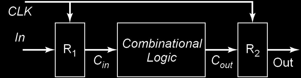
 Digital Integrated Circuits A Design Perspective Jan M. Rabaey Anantha Chandrakasan Borivoje Nikolić Timing Issues January 2003 1 Synchronous Timing CLK In R Combinational 1 R Logic 2 C in C out Out 2
5. Sequential Logic x Computation Structures Part 1 Digital Circuits. Copyright 2015 MIT EECS
 5. Sequential Logic 6.004x Computation Structures Part 1 igital Circuits Copyright 2015 MIT EECS 6.004 Computation Structures L5: Sequential Logic, Slide #1 Something We Can t Build (Yet) What if you were
Digital System Clocking: High-Performance and Low-Power Aspects. Vojin G. Oklobdzija, Vladimir M. Stojanovic, Dejan M. Markovic, Nikola M.
 Digital System Clocking: High-Performance and Low-Power Aspects Vojin G. Oklobdzija, Vladimir M. Stojanovic, Dejan M. Markovic, Nikola M. Nedovic Wiley-Interscience and IEEE Press, January 2003 Nov. 14,
Issues on Timing and Clocking
 ECE152B TC 1 Issues on Timing and Clocking X Combinational Logic Z... clock clock clock period ECE152B TC 2 Latch and Flip-Flop L CK CK 1 L1 1 L2 2 CK CK CK ECE152B TC 3 Clocking X Combinational Logic...
The Linear-Feedback Shift Register
 EECS 141 S02 Timing Project 2: A Random Number Generator R R R S 0 S 1 S 2 1 0 0 0 1 0 1 0 1 1 1 0 1 1 1 0 1 1 0 0 1 1 0 0 The Linear-Feedback Shift Register 1 Project Goal Design a 4-bit LFSR SPEED, SPEED,
Lecture 4: Technology Scaling
 Digital Integrated Circuits (83-313) Lecture 4: Technology Scaling Semester B, 2016-17 Lecturer: Dr. Adam Teman TAs: Itamar Levi, Robert Giterman 2 April 2017 Disclaimer: This course was prepared, in its
GMU, ECE 680 Physical VLSI Design 1
 ECE680: Physical VLSI Design Chapter VII Timing Issues in Digital Circuits (chapter 10 in textbook) GMU, ECE 680 Physical VLSI Design 1 Synchronous Timing (Fig. 10 1) CLK In R Combinational 1 R Logic 2
ALU, Latches and Flip-Flops
 CSE14: Components and Design Techniques for Digital Systems ALU, Latches and Flip-Flops Tajana Simunic Rosing Where we are. Last time: ALUs Plan for today: ALU example, latches and flip flops Exam #1 grades
Reducing Delay Uncertainty in Deeply Scaled Integrated Circuits Using Interdependent Timing Constraints
 Reducing Delay Uncertainty in Deeply Scaled Integrated Circuits Using Interdependent Timing Constraints Emre Salman and Eby G. Friedman Department of Electrical and Computer Engineering University of Rochester
EE141. Lecture 28 Multipliers. Lecture #20. Project Phase 2 Posted. Sign up for one of three project goals today
 EE141-pring 2008 igital Integrated ircuits Lecture 28 Multipliers 1 Announcements Project Phase 2 Posted ign up for one of three project goals today Graded Phase 1 and Midterm 2 will be returned next Fr
Sequential vs. Combinational
 Sequential Circuits Sequential vs. Combinational Combinational Logic: Output depends only on current input TV channel selector (-9) inputs system outputs Sequential Logic: Output depends not only on current
Topics. Dynamic CMOS Sequential Design Memory and Control. John A. Chandy Dept. of Electrical and Computer Engineering University of Connecticut
 Topics Dynamic CMOS Sequential Design Memory and Control Dynamic CMOS In static circuits at every point in time (except when switching) the output is connected to either GND or V DD via a low resistance
ELCT201: DIGITAL LOGIC DESIGN
 ELCT201: DIGITAL LOGIC DESIGN Dr. Eng. Haitham Omran, haitham.omran@guc.edu.eg Dr. Eng. Wassim Alexan, wassim.joseph@guc.edu.eg Lecture 6 Following the slides of Dr. Ahmed H. Madian محرم 1439 ه Winter
Adders, subtractors comparators, multipliers and other ALU elements
 CSE4: Components and Design Techniques for Digital Systems Adders, subtractors comparators, multipliers and other ALU elements Adders 2 Circuit Delay Transistors have instrinsic resistance and capacitance
Sequential Logic Design: Controllers
 Sequential Logic Design: Controllers Controller Design, Flip Flop Timing Copyright (c) 2012 Sean Key Standard Controller Architecture Controller A circuit that implements a FSM is referred to as a controller
Lecture 27: Latches. Final presentations May 8, 1-5pm, BWRC Final reports due May 7 Final exam, Monday, May :30pm, 241 Cory
 EE241 - Spring 2008 Advanced Digital Integrated Circuits Lecture 27: Latches Timing Announcements Wrapping-up the class: Final presentations May 8, 1-5pm, BWRC Final reports due May 7 Final exam, Monday,
EE241 - Spring 2007 Advanced Digital Integrated Circuits. Announcements
 EE241 - Spring 2007 Advanced Digital Integrated Circuits Lecture 25: Synchronization Timing Announcements Homework 5 due on 4/26 Final exam on May 8 in class Project presentations on May 3, 1-5pm 2 1 Project
EET 310 Flip-Flops 11/17/2011 1
 EET 310 Flip-Flops 11/17/2011 1 FF s and some Definitions Clock Input: FF s are controlled by a trigger or Clock signal. All FF s have a clock input. If a device which attempts to do a FF s task does not
ESE 570: Digital Integrated Circuits and VLSI Fundamentals
 ESE 570: Digital Integrated Circuits and VLSI Fundamentals Lec 18: March 27, 2018 Dynamic Logic, Charge Injection Lecture Outline! Sequential MOS Logic " D-Latch " Timing Constraints! Dynamic Logic " Domino
Chapter 13. Clocked Circuits SEQUENTIAL VS. COMBINATIONAL CMOS TG LATCHES, FLIP FLOPS. Baker Ch. 13 Clocked Circuits. Introduction to VLSI
 Chapter 13 Clocked Circuits SEQUENTIAL VS. COMBINATIONAL CMOS TG LATCHES, FLIP FLOPS SET-RESET (SR) ARBITER LATCHES FLIP FLOPS EDGE TRIGGERED DFF FF TIMING Joseph A. Elias, Ph.D. Adjunct Professor, University
Memory, Latches, & Registers
 Memory, Latches, & Registers 1) Structured Logic Arrays 2) Memory Arrays 3) Transparent Latches 4) How to save a few bucks at toll booths 5) Edge-triggered Registers L13 Memory 1 General Table Lookup Synthesis
Introduction EE 224: INTRODUCTION TO DIGITAL CIRCUITS & COMPUTER DESIGN. Lecture 6: Sequential Logic 3 Registers & Counters 5/9/2010
 EE 224: INTROUCTION TO IGITAL CIRCUITS & COMPUTER ESIGN Lecture 6: Sequential Logic 3 Registers & Counters 05/10/2010 Avinash Kodi, kodi@ohio.edu Introduction 2 A Flip-Flop stores one bit of information
CPE100: Digital Logic Design I
 Chapter 3 Professor Brendan Morris, SEB 3216, brendan.morris@unlv.edu http://www.ee.unlv.edu/~b1morris/cpe1/ CPE1: Digital Logic Design I Section 14: Dr. Morris Sequential Logic Design Chapter 3 Chapter
CSE140: Components and Design Techniques for Digital Systems. Midterm Information. Instructor: Mohsen Imani. Sources: TSR, Katz, Boriello & Vahid
 CSE140: Components and Design Techniques for Digital Systems Midterm Information Instructor: Mohsen Imani Midterm Topics In general: everything that was covered in homework 1 and 2 and related lectures,
Topics. CMOS Design Multi-input delay analysis. John A. Chandy Dept. of Electrical and Computer Engineering University of Connecticut
 Topics CMO Design Multi-input delay analysis pring 25 Transmission Gate OUT Z OUT Z pring 25 Transmission Gate OUT When is low, the output is at high impedance When is high, the output follows However,
Xarxes de distribució del senyal de. interferència electromagnètica, consum, soroll de conmutació.
 Xarxes de distribució del senyal de rellotge. Clock skew, jitter, interferència electromagnètica, consum, soroll de conmutació. (transparències generades a partir de la presentació de Jan M. Rabaey, Anantha
Clock signal in digital circuit is responsible for synchronizing the transfer to the data between processing elements.
 1 2 Introduction Clock signal in digital circuit is responsible for synchronizing the transfer to the data between processing elements. Defines the precise instants when the circuit is allowed to change
Digital Logic Design - Chapter 4
 Digital Logic Design - Chapter 4 1. Analyze the latch circuit shown below by obtaining timing diagram for the circuit; include propagation delays. Y This circuit has two external input and one feedback
ALU A functional unit
 ALU A functional unit that performs arithmetic operations such as ADD, SUB, MPY logical operations such as AND, OR, XOR, NOT on given data types: 8-,16-,32-, or 64-bit values A n-1 A n-2... A 1 A 0 B n-1
Lecture 9: Interconnect
 Digital Integrated Circuits (83-313) Lecture 9: Interconnect Semester B, 2016-17 Lecturer: Dr. Adam Teman TAs: Itamar Levi, Robert Giterman 23 May 2017 Disclaimer: This course was prepared, in its entirety,
Synchronous Sequential Logic
 1 IT 201 DIGITAL SYSTEMS DESIGN MODULE4 NOTES Synchronous Sequential Logic Sequential Circuits - A sequential circuit consists of a combinational circuit and a feedback through the storage elements in
Lecture 7: Logic design. Combinational logic circuits
 /24/28 Lecture 7: Logic design Binary digital circuits: Two voltage levels: and (ground and supply voltage) Built from transistors used as on/off switches Analog circuits not very suitable for generic
EE371 - Advanced VLSI Circuit Design
 EE371 - Advanced VLSI Circuit Design Midterm Examination May 7, 2002 Name: No. Points Score 1. 18 2. 22 3. 30 TOTAL / 70 In recognition of and in the spirit of the Stanford University Honor Code, I certify
P2 (10 points): Given the circuit below, answer the following questions:
: Given the circuit below, answer the following questions:") P1 (10 points): Given the function f(a, b, c, d) = m(3,4,5,10,14) + D(6,7): A: Fill in the timing diagram for f. B: Implement f using only 2-1 MUXes. Your circuit should not include more than four 2-1
P1 (10 points): Given the function f(a, b, c, d) = m(3,4,5,10,14) + D(6,7): A: Fill in the timing diagram for f. B: Implement f using only 2-1 MUXes. Your circuit should not include more than four 2-1
Time Allowed 3:00 hrs. April, pages
 IGITAL ESIGN COEN 32 Prof. r. A. J. Al-Khalili Time Allowed 3: hrs. April, 998 2 pages Answer All uestions No materials are allowed uestion a) esign a half subtractor b) esign a full subtractor c) Using
Timing Constraints in Sequential Designs. 63 Sources: TSR, Katz, Boriello & Vahid
 Timing Constraints in Sequential esigns 63 Sources: TSR, Katz, Boriello & Vahid Where we are now. What we covered last time: FSMs What we ll do next: Timing constraints Upcoming deadlines: ZyBook today:
Skew-Tolerant Circuit Design
 Skew-Tolerant Circuit Design David Harris David_Harris@hmc.edu December, 2000 Harvey Mudd College Claremont, CA Outline Introduction Skew-Tolerant Circuits Traditional Domino Circuits Skew-Tolerant Domino
Lecture 11: MOSFET Modeling
 Digital Integrated Circuits (83-313) Lecture 11: MOSFET ing Semester B, 2016-17 Lecturer: Dr. Adam Teman TAs: Itamar Levi, Robert Giterman 18 June 2017 Disclaimer: This course was prepared, in its entirety,
EE241 - Spring 2006 Advanced Digital Integrated Circuits
 EE241 - Spring 2006 Advanced Digital Integrated Circuits Lecture 20: Asynchronous & Synchronization Self-timed and Asynchronous Design Functions of clock in synchronous design 1) Acts as completion signal
Fundamentals of Computer Systems
 Fundamentals of Computer Systems Review for the Midterm Stephen A. Edwards Columbia University Spring 22 The Midterm 75 minutes 4 5 problems Closed book Simple calculators are OK, but unnecessary One double-sided
Fundamentals of Computer Systems
 Fundamentals of Computer Systems Review for the Final Stephen A. Edwards Columbia University Summer 25 The Final 2 hours 8 problems Closed book Simple calculators are OK, but unnecessary One double-sided
CHAPTER 9: SEQUENTIAL CIRCUITS
 CHAPTER 9: ASYNCHRONOUS SEUENTIAL CIRCUITS Chapter Objectives 2 Sequential circuits that are not snchronized b a clock Asnchronous circuits Analsis of Asnchronous circuits Snthesis of Asnchronous circuits
Sequential Logic Circuits
 Chapter 4 Sequential Logic Circuits 4 1 The defining characteristic of a combinational circuit is that its output depends only on the current inputs applied to the circuit. The output of a sequential circuit,
Methodology to Achieve Higher Tolerance to Delay Variations in Synchronous Circuits
 Methodology to Achieve Higher Tolerance to Delay Variations in Synchronous Circuits Emre Salman and Eby G. Friedman Department of Electrical and Computer Engineering University of Rochester Rochester,
Chapter 7 Sequential Logic
 Chapter 7 Sequential Logic SKEE2263 Digital Systems Mun im/ismahani/izam {munim@utm.my,e-izam@utm.my,ismahani@fke.utm.my} March 28, 2016 Table of Contents 1 Intro 2 Bistable Circuits 3 FF Characteristics
Adders, subtractors comparators, multipliers and other ALU elements
 CSE4: Components and Design Techniques for Digital Systems Adders, subtractors comparators, multipliers and other ALU elements Instructor: Mohsen Imani UC San Diego Slides from: Prof.Tajana Simunic Rosing
University of Toronto Faculty of Applied Science and Engineering Edward S. Rogers Sr. Department of Electrical and Computer Engineering
 University of Toronto Faculty of Applied Science and Engineering Edward S. Rogers Sr. Department of Electrical and Computer Engineering Final Examination ECE 241F - Digital Systems Examiners: J. Rose and
UNIVERSITY OF CALIFORNIA, BERKELEY College of Engineering Department of Electrical Engineering and Computer Sciences
 UNIVERSITY OF CALIFORNIA, BERKELEY College of Engineering Department of Electrical Engineering and Computer Sciences Elad Alon Homework #9 EECS141 PROBLEM 1: TIMING Consider the simple state machine shown
LECTURE 28. Analyzing digital computation at a very low level! The Latch Pipelined Datapath Control Signals Concept of State
 Today LECTURE 28 Analyzing digital computation at a very low level! The Latch Pipelined Datapath Control Signals Concept of State Time permitting, RC circuits (where we intentionally put in resistance
EE141Microelettronica. CMOS Logic
 Microelettronica CMOS Logic CMOS logic Power consumption in CMOS logic gates Where Does Power Go in CMOS? Dynamic Power Consumption Charging and Discharging Capacitors Short Circuit Currents Short Circuit
Laboratory Exercise #8 Introduction to Sequential Logic
 Laboratory Exercise #8 Introduction to Sequential Logic ECEN 248: Introduction to Digital Design Department of Electrical and Computer Engineering Texas A&M University 2 Laboratory Exercise #8 1 Introduction
Latches. October 13, 2003 Latches 1
 Latches The second part of CS231 focuses on sequential circuits, where we add memory to the hardware that we ve already seen. Our schedule will be very similar to before: We first show how primitive memory
TAU 2014 Contest Pessimism Removal of Timing Analysis v1.6 December 11 th,
 TU 2014 Contest Pessimism Removal of Timing nalysis v1.6 ecember 11 th, 2013 https://sites.google.com/site/taucontest2014 1 Introduction This document outlines the concepts and implementation details necessary
Chapter 4. Sequential Logic Circuits
 Chapter 4 Sequential Logic Circuits 1 2 Chapter 4 4 1 The defining characteristic of a combinational circuit is that its output depends only on the current inputs applied to the circuit. The output of
Introduction to Digital Logic
 Introduction to Digital Logic Lecture 17: Latches Flip-Flops Problem w/ Bistables Output should have been at end of sequence Problem: Glitch was remembered Need some way to ignore inputs until they are
Lecture 1: Circuits & Layout
 Lecture 1: Circuits & Layout Outline q A Brief History q CMOS Gate esign q Pass Transistors q CMOS Latches & Flip-Flops q Standard Cell Layouts q Stick iagrams 2 A Brief History q 1958: First integrated
Sequential Circuits. Circuits with state. Silvina Hanono Wachman Computer Science & Artificial Intelligence Lab M.I.T. L06-1
 Sequential Circuits Circuits with state Silvina Hanono Wachman Computer Science & Artificial Intelligence Lab M.I.T. L06-1 Combinational circuits A 0 A 1 A n-1. Sel lg(n) O Mux A B Comparator Result: LT,
Sequential Logic. Handouts: Lecture Slides Spring /27/01. L06 Sequential Logic 1
 Sequential Logic Handouts: Lecture Slides 6.4 - Spring 2 2/27/ L6 Sequential Logic Roadmap so far Fets & voltages Logic gates Combinational logic circuits Sequential Logic Voltage-based encoding V OL,
LOGIC CIRCUITS. Basic Experiment and Design of Electronics. Ho Kyung Kim, Ph.D.
 Basic Experiment and Design of Electronics LOGIC CIRCUITS Ho Kyung Kim, Ph.D. hokyung@pusan.ac.kr School of Mechanical Engineering Pusan National University Digital IC packages TTL (transistor-transistor
UMBC. At the system level, DFT includes boundary scan and analog test bus. The DFT techniques discussed focus on improving testability of SAFs.
 Overview Design for testability(dft) makes it possible to: Assure the detection of all faults in a circuit. Reduce the cost and time associated with test development. Reduce the execution time of performing
Sequential Logic. Road Traveled So Far
 Comp 2 Spring 25 2/ Lecture page Sequential Logic These must be the slings and arrows of outrageous fortune ) Synchronous as an implementation of Sequential 2) Synchronous Timing Analysis 3) Single synchronous
State and Finite State Machines
 State and Finite State Machines See P&H Appendix C.7. C.8, C.10, C.11 Hakim Weatherspoon CS 3410, Spring 2013 Computer Science Cornell University Big Picture: Building a Processor memory inst register
ECEN 248: INTRODUCTION TO DIGITAL SYSTEMS DESIGN. Week 7 Dr. Srinivas Shakkottai Dept. of Electrical and Computer Engineering
 ECEN 248: INTRODUCTION TO DIGITAL SYSTEMS DESIGN Week 7 Dr. Srinivas Shakkottai Dept. of Electrical and Computer Engineering SEQUENTIAL CIRCUITS: LATCHES Overview Circuits require memory to store intermediate
S.Y. Diploma : Sem. III [DE/ED/EI/EJ/EN/ET/EV/EX/IC/IE/IS/IU/MU] Principles of Digital Techniques
![S.Y. Diploma : Sem. III [DE/ED/EI/EJ/EN/ET/EV/EX/IC/IE/IS/IU/MU] Principles of Digital Techniques](/thumbs/82/86792063.jpg "S.Y. Diploma : Sem. III [DE/ED/EI/EJ/EN/ET/EV/EX/IC/IE/IS/IU/MU] Principles of Digital Techniques") S.Y. Diploma : Sem. III [DE/ED/EI/EJ/EN/ET/EV/EX/IC/IE/IS/IU/MU] Principles of Digital Techniques Time: 3 Hrs.] Prelim Question Paper Solution [Marks : 100 Q.1(a) Attempt any SIX of the following : [12]
S.Y. Diploma : Sem. III [DE/ED/EI/EJ/EN/ET/EV/EX/IC/IE/IS/IU/MU] Principles of Digital Techniques Time: 3 Hrs.] Prelim Question Paper Solution [Marks : 100 Q.1(a) Attempt any SIX of the following : [12]
Digital Design. Sequential Logic
 Principles Of igital esign Chapter 6 Sequential Logic Chapter preview Boolean algebra 3 Logic gates and flip-flops 3 Finite-state machine 6 Logic design techniques 4 Sequential design techniques 6 Binary
MOSIS REPORT. Spring MOSIS Report 1. MOSIS Report 2. MOSIS Report 3
 MOSIS REPORT Spring 2010 MOSIS Report 1 MOSIS Report 2 MOSIS Report 3 MOSIS Report 1 Design of 4-bit counter using J-K flip flop I. Objective The purpose of this project is to design one 4-bit counter
ESE 570: Digital Integrated Circuits and VLSI Fundamentals
 ESE 570: Digital Integrated Circuits and VLSI Fundamentals Lec 17: March 23, 2017 Energy and Power Optimization, Design Space Exploration, Synchronous MOS Logic Lecture Outline! Energy and Power Optimization
Homework 2 due on Wednesday Quiz #2 on Wednesday Midterm project report due next Week (4 pages)
") EE241 - Spring 2013 Advanced Digital Integrated Circuits Lecture 12: SRAM Design ECC Timing Announcements Homework 2 due on Wednesday Quiz #2 on Wednesday Midterm project report due next Week (4 pages)
EE241 - Spring 2013 Advanced Digital Integrated Circuits Lecture 12: SRAM Design ECC Timing Announcements Homework 2 due on Wednesday Quiz #2 on Wednesday Midterm project report due next Week (4 pages)
CSE241 VLSI Digital Circuits Winter Lecture 07: Timing II
 CSE241 VLSI Digital Circuits Winter 2003 Lecture 07: Timing II CSE241 L3 ASICs.1 Delay Calculation Cell Fall Cap\Tr 0.05 0.2 0.5 0.01 0.02 0.16 0.30 0.5 2.0 0.04 0.32 0.178 0.08 0.64 0.60 1.20 0.1ns 0.147ns
Lecture 14: State Tables, Diagrams, Latches, and Flip Flop
 EE210: Switching Systems Lecture 14: State Tables, Diagrams, Latches, and Flip Flop Prof. YingLi Tian Nov. 6, 2017 Department of Electrical Engineering The City College of New York The City University
Menu. Master-Slave Flip-Flop
 Menu Clocks and Master-lave Flip-Flops J-K and other Flip-Flops Truth table & excitation table Adders (see [Lam: pg 130]) Counters Look into my... 1 CLK Master-lave Flip-Flop Master-lave Latch/Flip-Flop