SAU1A FUNDAMENTALS OF DIGITAL COMPUTERS
|
|
|
- George Glenn
- 5 years ago
- Views:
Transcription

1 SAU1A FUNDAMENTALS OF DIGITAL COMPUTERS Unit : I - V
2 Unit : I Overview Fundamentals of Computers Characteristics of Computers Computer Language Operating Systems Generation of Computers 2
3 Definition of a Computer A computer is an electronic device that operates under the control of a set of instructions that is stored in its memory unit. A computer accepts data from an input device and processes it into useful information which it displays on its output device. Actually, a computer is a collection of hardware and software components that help you to accomplish many different tasks. 1. Hardware consists of the computer itself, and any equipment connected to it. 2. Software is the set of instructions that the computer follows in performing a task. 3

4 Components of a Computer 4 4
5 Functional Components of a Computer 1. INPUT DEVICES - Devices that allow the user to enter information into the PC (keyboard, mouse, scanner, etc.) 2. OUTPUT DEVICES - Devices that allow the computer to communicate with the user (monitor, printer, etc.) 3. CPU - The CPU consists of electronic circuits that interpret and execute instructions; it communicates with the input, output, and storage devices. 4. Memory - or primary storage, works with the CPU to hold instructions and data in order to be processed. 5
6 Storage Devices Shape Name Capacity Drive Letter (usually) Characteristics 3 ½ Diskette 1.44 Megabytes A: or B: Recordable, Very slow, Tend to lose information easily, Very cheap, Exchangeable, Easy to carry. Hard Disk Drive Between 1 and 16 Gigabytes C: Recordable, Very fast, Boot disk, Safe, Very Expensive. ZIP or LS-120 Between 100 Megabytes and 1 Gigabyte D:, E:, F: Recordable, Fast, Safe, Very Expensive, Exchangeable, Easy to carry. CD-ROM 650 Megabytes (0.65 Gigabytes) D:, E:, F: Some Recordable (expensive), Capacity for Audio, Very Fast, Very Safe, Cheap, Easy to carry. DVD-ROM Up to 17 Gigabytes (Up to Megabytes) D:, E:, F: New, Capacity for Audio and Video, Very Fast, Very Safe, Very Expensive, Easy to carry. 7
7 Characteristics of a Computer Speed Memory Diligence Versatility Lack of Decision making 8
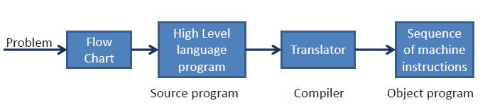
8 Computer Languages Programming languages can be classified as: 1. Machine language The only language understood by computers. It comprises entirely of numbers. 2. Assembly language Similar to machine languages, but enable the use of names instead of numbers. Assembly language is converted to machine language using an interpreter. 3. High-level language Closer to human languages, easier to read, write and maintain. High-level language is converted to Assembly language using a compiler or assembler. Eg. C, C++, Cobol, Fortran, Java 4. Fourth-generation language 4GL is more closer to human languages than typical high-level languages. Most 4GLs are used to access databases. 10

9 Computer Language 11
10 Operating System The operating system is the software that provides an interface between the hardware (the computer itself) and the user. It manages the hardware and enables the user to control the computer. Microsoft developed the first operating system for IBM machines, MS DOS (Microsoft Disk Operating System), the grandfather of the current DOS and Windows systems. The IBM family is based on the Intel 8086 family of chips, which evolved into the high-speed Pentium chips of today. At the same time, the Apple Computer Company started Macintosh series based on the Motorola family of microprocessor chips. 12
11 Generations of Computers The history of computer development is often referred to in reference to the different generations of computing devices. Each generation of computer is characterized by a major technological development that fundamentally changed the way computers operate, resulting in increasingly smaller, cheaper, more powerful and more efficient and reliable devices. Based on the above mentioned features, we have five generations of computers. Generations of Computers 14
12 Number System Binary System Binary Code Logic Gates Unit : II Overview 15
13 The larger the base, more the numerals required: Number System Base Digits or Symbols included Binary 2 0,1 Decimal 10 0,1,2,3,4,5,6,7,8,9 Octal 8 0,1,2,3,4,5,6,7 Hexadecimal 16 0,1,2,3,4,5,6,7,8,9, A,B,C,D,E,F The range of possible numbers for each system is R=BK, where B = Base, K = number of digits For example, a 16-bit PC will have R = 2 16 = 65,536 different values. 16
14 Conversion from Decimal to other system Step 1 : Repeatedly, divide the integer part by the base to which it has to be converted, and collect the remainders in the reverse direction. Step 2 : Successively, multiply the fractional part by the base to which it has to be converted, and collect the carries from top to bottom. If the fractional part is not zero after 4 or 5 steps, the process can be stopped. Examples: 1. Convert (19.625) 10 to its binary equivalent. 19 / 2 = 9; remainder = 1 9 / 2 = 4; remainder = 1 4 / 2 = 2; remainder = 0 2 / 2 = 1; remainder = 0 1 / 2 = 0; remainder = 1 Thus, (19.625) 10 = ( ) x 2 = 1.250; carry = x 2 = 0.500; carry = x 2 = 1.000; carry = 1 18
15 Conversion from Binary to Octal / Hexadecimal Step 1 : Arrange the given number into groups of 3 bits (Octal) or 4 bits (Hexadecimal), starting from the Least Significant Bit (LSB). If the final group has lesser number of bits, include 0s. Step 2 : Replace each group with its octal or hexadecimal equivalent, as required. Example: Convert ( ) 2 to octal and hexadecimal equivalents. ( ) 2 = ( ) 2 = ( ) 8 = (36.6) 8 ( ) 2 = ( ) 2 = ( 1 E. C) 16 = (1E.C) 16 19
16 Conversion from Octal / Hexadecimal to Binary These conversions are the simplest of all. Replace each octal or hexadecimal digit with its binary equivalent. Examples: 1. Convert (3D.E8) 16 to its binary equivalent. (3D.E8) 16 = ( ) 2 2. Convert (45.5) 8 to its binary equivalent. (45.5) 8 = ( ) 2 20
17 Binary Arithmetic Rules for Binary Addition = = 1 ; = = 0 ; Carry = = 1 ; Carry = 1 Example: 1. Add 3 and > 011 Augend 4 -> Addend > 111 Result 2. Add 13 and > 1101 Augend 7 -> Addend > Result 21
18 Complements There are 2 types of complements used in Binary System, namely 1 s Complement and 2 s Complement. Complements are also used to represent negative numbers. 1 s Complement: 1 s Complement of a bit can be obtained as 1 minus that bit. i.e. 1 s complement of 1 is 1 1 = 0 and 1 s complement of 0 is 1 0 = 1. In general, invert the given bit to get its 1 s complement. 2 s Complement: 2 s Complement of a bit is obtained by adding 1 to the 1 s complement of that bit. i.e. 2 s Complement of > 1 s complement of > =
19 Signed Binary Numbers To represent the sign of the given number, we will use a separate bit (sign bit). It becomes the MSB of the binary number. The bit 0 represents (+) or positive numbers and the bit 1 represents (-) or negative numbers. Negative numbers are represented in either of the following ways: 1. Sign-Magnitude The MSB represents the sign and the remaining bits represent the magnitude of the number. Example: +5 = = = = Note: Positive numbers are represented only using the signmagnitude form 23
20 1 s Co ple e t Su tra tio Contd. Example 1: Subtract 4 from > 1101 ; 4 -> s complement of 4 -> Adding carry, result is 1001 i.e. +9 Example 2: Subtract 13 from > 0100 ; 13 -> s complement of 13 -> No carry -> result is negative. Take 1 s complement of > 1001 Thus, result is -9 24
21 2 s Complement Subtraction Contd. Example 1: Subtract 4 from > 1101 ; 4 -> s complement of 4 -> = Ignore carry, result is 1001 i.e. +9 Example 2: Subtract 13 from > 0100 ; 13 -> s complement of 13 -> No carry -> result is negative. Take 2 s complement of > i.e Thus, result is -9 25
22 Binary Codes Codes are alternate representations for the binary numbers. Different codes are used for binary numbers. Commonly used are 1. BCD (Binary Coded Decimal) Code a) 8421 b) 2421 c) Excess-3 Code 3. Gray Code 26
23 Logic Gates and Truth Tables Any logic circuit can be implemented using the following basic gates: 1. NOT Gate 2. OR Gate 3. AND Gate Each of the Gates can be represented schematically, or as an expression, or as a truth table. Other gates can be implemented as a combination of the basic gates. For the given logic circuit, we can get the Boolean expression and then form the truth table. Also for the given truth table, we can get the Boolean expression and then construct the logic circuit. 30
24 NOT Gate This function operates on a single Boolean value. Its output is the complement of its input. i.e. Output Y = X An input of 1 produces an output of 0 and an input of 0 produces an output of 1. X Y = X x x' Output is 1 if at least one input is 1. More than two values can be or-ed together. For example x + y + z = 1 if at least one of the three values is 1. x y out = x+y x y out
25 AND Gate Output is one if every input has value of 1. More than two values can be and-ed together. For example xyz = 1 only if x=1, y=1 and z=1. x y out = xy x y out 33
26 NAND Gate When the output of AND gate is given as input to the NOT gate (or a bubble can be added to the AND gate), the result circuit is the NAND gate. The output of the NAND gate is the complement of the output of the AND gate. x y out = (xy) When the output of OR gate is given as input to the NOT gate (or a bubble can be added to the AND gate), the result circuit is the NOR gate. The output of the NOR gate is the complement of the output of the OR gate. x y x y out x y out = (x + y) out 34
27 EX-OR (Exclusive-OR) Gate The output of the XOR gate is equal to 1, if an odd number of input values are 1 and 0 if an even number of input values are 1. x y out = x y The output of the XNOR gate is the complement of the output of the XOR gate. x y out x y out = x out y 36
28 X Manipulating Boolean Functions Given Logic Circuit: y z xy'+yz 38
29 We can express it as: f(x,y,z) = xy + yz The truth table is: x y z xy' yz xy + yz
30 Unit : III Overview Boolean Algebra Truth Tables Universal Gates Simplification of Boolean functions Map Methods Mc-Clausky Tabulation Methods 40
31 Boolean Algebra Using Boolean laws helps to reduce the given function to a lesser number of literals. Also a lesser number of gates. Result More efficient and cheaper digital circuits. The simplification can be achieved using the various axioms and laws of Boolean Algebra 41
32 Laws similar to Ordinary Algebra Commutative Law A + B = B + A A. B = B. A Associative Law A + (B + C) = (A + B) + C A (BC) = (AB) C Distributive Law A (B + C) = AB + AC Boolean Axioms 42
33 Rules specific to Boolean Algebra 1. a) A + 0 = A b) A. 1 = A When A = 0 When A = 0 A + 0 = = 0 = A A. 1 = 0. 1 = 0 = A When A = 1 When A = 1 A + 0 = = 1 = A A. 1 = 1. 1 = 1 = A 2. a) A + 1 = 1 b) A. 0 = 0 When A = 0 When A = 0 When A = 1 A + 1 = = 1 A + 1 = = 1 When A = 1 A. 0 = 0. 0 = 0 A. 0 = 1. 0 = 0 43
34 Rules specific to Boolean Algebra 3. a) A + A = A b) A. A = A When A = 0 A + A = = 0 = A When A = 1 A + A = = 1 = A When A = 0 A. A = 0. 0 = 0 = A When A = 1 A. A = 1. 1 = 1 = A 4. a) A + A = 1 b) A. A = 0 When A = 0 A + A = = 1 When A = 1 A + A = = 1 When A = 0 A. A = 0. 1 = 0 When A = 1 A. A = 1. 0 = 0 44
35 Rules specific to Boolean Algebra 5. a) A = A When A = 0 When A = 1 A = 1 ; A = 0 = A A = 0 ; A = 1 = A This double complement rule is also known as Involution 45
36 Rules specific to Boolean Algebra 6. a) A + AB = A b) A (A + B) = A L.H.S = A + AB = A (1 + B) Distributive law = A. 1 Since, 1 + B = 1 = A Since, A. 1 = A = R.H.S L.H.S = A (A + B) = AA + AB Distributive law = A + AB Since, AA = A = A Since, A + AB = A = R.H.S 46
37 Rules specific to Boolean Algebra 7. a) A + A B = A + B b) A (A + B) = AB L.H.S = A + A B = A.1 + A B Since, A.1=A = A.(1 + B) + A B Since, 1+B=1 = A + AB + A B Distributive law = A + B (A + A ) Distributive law = A + B Since, A + A = 1 = R.H.S L.H.S = A (A + B) = A.A + AB Distributive law = 0 + AB Since, A. A = 0 = AB Since, 0 + AB = AB = R.H.S 47
38 Rules specific to Boolean Algebra 8. a) A + BC = (A + B) (A + C) R.H.S = (A + B) (A + C) = AA + BA + AC + BC = A + AB + AC + BC Since, A.A=A ; AB = BA = A (1 + B + C) + BC Distributive Law = A + BC Since, 1 + A + = 1 & A.1 = 1 = L.H.S b) A ( B + C) = AB + AC This is the Distributive Law. 48
39 Rules specific to Boolean Algebra 9. a) AB + A C + BC = AB + A C Hint: We need to remove BC from L.H.S LHS = AB + A C + BC = AB + A C + BC. 1 Since, 1.BC = BC = AB + A C + BC (A + A ) Since, A + A = 1 = AB + A C + ABC + A BC Distributive law = AB (1 + C) + A C (1 + B) = AB + A C = RHS 49
40 Rules specific to Boolean Algebra b) (A+B) (A +C) (B+C) = (A+B) (A +C) LHS = (A + B) (A + C) (B + C) = (AA + A B + AC + BC) (B + C) = (A B + AC + BC) (B + C) Since, AA =0 = A BB + ABC + BBC + A BC + ACC + BCC = A B + A BC + ABC + BC + AC + BC Since, BB=B = A B (1 + C) + BC (A + 1) + AC + BC = A B + BC + AC + BC Since, 1+C=1 = A B + AC + BC RHS = (A + B) (A + C) = AA + A B + AC + BC = A B + AC + BC = LHS 50
41 Demorgan s Laws The AND and OR functions can be shown to be related to each other through the following equations. Theorem 1: The complement of a product is equal to the sum of individual complements. In other words, (AB) = A + B NAND = Bubbled OR or Theorem 2: The complement of a sum is equal to the product of individual complements. In other words, (A + B) = A. B or NOR = Bubbled AND 51
42 For Example: 1. Simplify: Find the complement of AB + C D and simplify. Solution: (AB + C D ) = (AB ). (C D ) = (A + B). (C + D ) = (A + B). (C + D) 2. Show that (A B + AB ) = A B + AB Solution: LHS = (A B + AB ) = (A B). (AB ) = (A + B ). (A + B ) = (A + B ). (A + B) = AA + A B + AB + BB = A B + AB Since, AA = 0 and BB = 0 52
43 Universal Gates Universal gates are the ones which can be used for implementing any gate like AND, OR and NOT, or any combination of these basic gates. NAND and NOR gates are universal gates. But there are some rules that need to be followed when implementing NAND or NOR based gates. NAND as Universal Gate Any logic function can be implemented using NAND gates. To achieve this, first the logic function has to be written in Sum of Product (SOP) form. Once logic function is converted to SOP, the logic circuit with AND gates in first level and OR gates in second level can be converted into a NAND- NAND gate circuit. 53
44 Simplification of Boolean functions Simplification of Boolean functions is mainly used to reduce the gate count of a design. Less number of gates means less power consumption, sometimes the circuit works faster. When number of gates is reduced, cost also comes down. There are many ways to simplify a logic design. 1. Algebraic Simplification - Simplify symbolically using theorems. 2. Karnaugh Maps Simplifies using Diagrammatic technique. 3. Quine-McCluskey Simplifies using Tabulation technique. 54
45 Karnaugh Maps (K-Maps) Karnaugh maps provide a systematic method to obtain simplified sum-ofproducts (SOPs) Boolean expressions. This is a compact way of representing a truth table and is a technique that is used to simplify logic expressions. It is ideally suited for four or less variables, becoming cumbersome for five or more variables. A K-map of n variables will have 2 n squares. Each square represents either a minterm or maxterm. For a Boolean expression, product terms are denoted by 1's, while sum terms are denoted by 0's - but 0's are often left blank. 55
 00, 01, 10, 11 or b) A B, A B, AB, AB or c) m0, m1, m2, m3 The K-Map can be drawn in either of the")
46 2 Variable K-Map A 2-variable K-Map will have 4 cells. The function can have 4 possible combinations. a) 00, 01, 10, 11 or b) A B, A B, AB, AB or c) m0, m1, m2, m3 The K-Map can be drawn in either of the following ways: 56

47 For example : F = X'Y+XY+XY' 1. Draw the k-map for function F with marking 1 for X'Y, XY and XY position. 2. Now combine two 1's as shown in figure to form the two single terms. F = X + Y 57
 000, 001, 010, 011, 100, 101, 110, 111 or b) A B C, A B C, A BC, A BC, AB C, AB C, ABC, ABC or c) m0, m1, m2, m3, m4, m5, m6, m7 The K-Map can be drawn as below: Using gray code arrangement")
48 3 Variable K-Map A 3-variable K-Map will have 8 cells. The function can have 8 possible combinations. a) 000, 001, 010, 011, 100, 101, 110, 111 or b) A B C, A B C, A BC, A BC, AB C, AB C, ABC, ABC or c) m0, m1, m2, m3, m4, m5, m6, m7 The K-Map can be drawn as below: Using gray code arrangement ensures that minterms of adjacent cells differ by only ONE literal. SAE2B Digital Electronics & Microprocessor 58

49 For example : F(X,Y,Z) = Σ(1,3,4,5,6,7) 1. Draw the k-map for function F with marking 1 for m1, m3, m4, m5, m6 and m7. 2. Now combine 1 s as shown in figure to form the reduced terms. F = X + Z 59

50 4 Variable K-Map A 4-variable K-Map will have 16 cells. The function can have 16 possible combinations m0 to m15. The K-Map can be drawn as below: 60
51 For example : F(A, B, C, D) = Σ(0, 1, 2, 3, 5, 7, 8, 9, 10, 11, 13, 15) 1. Draw the k-map for function F with marking 1 for the given minterms. 2. Now combine 1 s as shown in figure to form the reduced terms. AB CD F = B + D

52 5 Variable K-Map A 5-variable K-Map will have 32 cells m0 to m31. The 5-Variable Map can be drawn as 2 4-variable maps-m0 to m15 and m16 to m31. If the reduced expressions for the 2 individual maps is Y1 and Y2, we can write the final expression as Y = Y1 + Y2. If necessary, apply Boolean laws for further simplification. 62
53 For Example: F(A,B,C,D,E) = Σ(0,1,3,5,7,,9,11,13,15,16,17,20,21) A = 0 BC DE A = 1 DE BC The reduced expressions for the 2 maps are: Y1 = AB C D + AE and Y2 = A B D Thus, Y = AB C D + AE + A B D = B D (A + AC ) + AE = B D (A + C ) + AE = A B D + B C D + AE 63
54 Quine McCluskey Method Represent the expression in the canonical SOP form. Consider the function F(A,B,C,D) = Σ(0, 1, 4, 5, 10, 11, 14, 15) Step 1: Represent each minterm in binary as shown: Decimal Binary
55 Step 2: Arrange the minterms in different groups, so that the first group has no 1 s, second group contains only one 1, third group contains two 1 s and so on ; First Group ; Second Group ; Third Group ; Fourth Group ; Fifth Group 65
56 Step 3 : a) Each minterm of one group is compared with each minterm in the group immediately below. b) Each time a number is found in one group which is the same as a number in the group below except for one digit, the numbers pair is ticked and a new composite is created. c) This composite number has the same number of digits as the numbers in the pair except the digit different which is replaced by an "x". 66
57 Column 1 - A B C D Column 2 - A B C D (0,1) x (0,4) 0 x 0 0 (1,5) 0 x 0 1 (4,5) x (10,11) x (10,14) 1 x 1 0 (11,15) 1 x 1 1 (14,15) x 67
58 Step 4 : Repeat Step 3 on Column 2. Column 1 - A B C D Column 2 - A B C D Column 3 - A B C D (0,1) x (0,4) 0 x 0 0 (1,5) 0 x 0 1 (4,5) x (0,1,4,5) 0 x 0 x (0,4,1,5) 0 x 0 x (10,11) x (10,14) 1 x 1 0 (11,15) 1 x 1 1 (14,15) x (10,11,14,15) 1 x 1 x (10,14,11,15) 1 x 1 x 68
59 Sequential Logic Flip-Flops Shift Register Counters Unit : IV Overview 69
60 Sequential Logic The outputs of a sequential logic circuit depend on both the current inputs and on previous inputs and outputs of the circuit. Sequential elements have storage elements that record the state of the circuit. In other words, the state information combined with the inputs is generating the outputs. The state and inputs also combine to generate a new state of the circuit. The same inputs in a sequential circuit may generate different outputs and different new states, depending on the circuit s current state. 70
61 Flip-Flops A bi-stable device i.e. a circuit with only 2 stable states, namely the 0 state and the 1 state. Ability to retain its state and store a bit of information. It is one-bit memory cell. A flip-flop has 2 outputs and they complement each other. Types of Flip Flop SR Flip Flop, JK Flip Flop, D Flip Flop, T Flip Flop. 71
62 Shift Register A common form of register used in computers and in many other types of logic circuits is a shift register. It is simply a set of flip flops (usually D latches or RS flip-flops) connected together so that the output of one becomes the input of the next, and so on in series. It is called a shift register because the data is shifted through the register by one bit position on each clock pulse. 72


63 Serial-in Serial-out Register On the leading edge of the first clock pulse, the signal on the D input is latched in the first flip flop. On the leading edge of the next clock pulse, the contents of the first flip-flop is stored in the second flip-flop, and the signal which is present at the D input is stored is the first flip-flop, etc. Because the data is entered one bit at a time, this called a serial-in shift register. Since there is only one output, and data leaves the shift register one bit at a time, then it is also a serial out shift register. 73

64 Parallel-in Parallel-out Register Parallel input can be provided through the use of the preset and clear inputs to the flip-flop. The parallel loading of the flip-flop can be synchronous (i.e., occurs with the clock pulse) or asynchronous (independent of the clock pulse) depending on the design of the shift register. Parallel output can be obtained from the outputs of each flip-flop as shown in Figure. 74
65 Counters Counter is a register which counts the sequence in binary form. The state of counter changes with application of clock pulse. The counter is binary or non-binary. The total number of states in counter is called as modulus. If counter is modulus-n, then it has n different states. State diagram of counter is a pictorial representation of counter states directed by arrows in graph State diagram of mod-8 counter
66 Asynchronous (Ripple) Counters All Flip-Flops are in toggle mode. The clock input is applied. Count enable = 1. Counter counts from 0000 to
67 Synchronous Counter In synchronous counters, the clock inputs of all the flip-flops are connected together and are triggered by the input pulses. Thus, all the flip-flops change state simultaneously (in parallel). The J and K inputs of FF0 are connected to HIGH. FF1 has its J and K inputs connected to the output of FF0, and the J and K inputs of FF2 are connected to the output of an AND gate that is fed by the outputs of FF0 and FF1. After the 3rd clock pulse, both outputs of FF0 and FF1 are HIGH. The positive edge of the 4th clock pulse will cause FF2 to change its state due to the AND gate. 77
68 Up / Down Counter Bidirectional counters, also known as Up/Down counters, are capable of counting in either direction through any given count sequence and they can be reversed at any point within their count sequence by using an additional control input 78
69 Unit : IV Overview Adders,Subtractors Decoders,Encoders Multiplexer,Demultiplexer ROM PLA 79
70 HALF ADDER From our truth table, we can derive the following statement: Our adding circuit should consist of an XOR gate (for R output, the Sum line) and an AND gate (for Q output, the Carry line). INPUTS OUTPUTS Q R A B A B A B The XOR circuit delivers the Sum Line (R) of adding two single digits. The AND circuit produces the Carry Line (Q). We ve just created a fundamental circuit called a Half Adder, which provides the capability of adding two single bit numbers. 80


71 Circuit Diagram for the Half Adder A R SUM B Q CARRY 81
72 FULL ADDER The Half Adder operates as the key component in a divide-and-conquer approach to adding n digits. Three single digit numbers could be added two at a time: 1. Add the first two digits together using a half-adder. 2. Add the result of this sum to the third number using another half-adder. To achieve this, 1. We need 3 input lines, one for each number. 2. Two input lines feed into the first half adder; the third input line functions as a carry-in line. 3. The second half-adder has two input lines: the output sum from the first half-adder, plus the third, carry-in input line. 82
73 Truth Table for the Full Adder INPUTS OUTPUTS A B C IN Q CARRY R SUM
74 Subtractor What we have is a circuit that can add numbers. We want to make this circuit also work for subtracting two numbers Let s rethink our problem, with a specific example: 5-2 = 3, or, put another way: 5 + (-2) = 3 Now, we have an addition problem, instead of subtraction. This means our existing circuit will work if we could unlock how to represent negative numbers, like -2. This could be achieved using 2 s Complement. 84
75 Half Subtractor SAE2B Digital Electronics & Microprocessor 85
76 Full Subtractor To subtract the higher order columns you also need to subtract the borrow. The circuit can be constructed out of 2 half subtractors SAE2B Digital Electronics & Microprocessor 86
77 DECODERS A decoder is a combinational circuit that converts binary information from n inputs to exactly one output of a maximum of 2^n outputs. The maximum number of outputs is directly related to the number of inputs. A decoder with n inputs supports 2^n outputs. When n = 2, there are 2^2 = 4 outputs that can be decoded. When n = 3, there are 2^3 = 8 outputs that can be decoded. 87

78 Example: Design a 3 x 8 decoder using a truth table. Y0 = A B C Y1 = A B C Y2 = A BC Y3 = A BC Y4 = AB C Y5 = AB C Y6 = ABC Y7 = ABC 88
79 DEMULTIPLEXER A demultiplexer, sometimes abbreviated demux, is a circuit that has one input and more than one output. It is used when a circuit wishes to send a signal to one of many devices. This description sounds similar to the description given for a decoder, but a decoder is used to select among many devices while a demultiplexer is used to send a signal among many devices. 89
80 The truth table for a 1-to-2 demultiplexer is I A D 0 D Using our 1-to-2 decoder as part of the circuit, we can express this circuit easily
81 Design of Circuit using MUX Multiplexers can be used in the design of both complex circuits and also realization of primitive gates such as XOR and AND gates. XOR gate: If we look at an XOR gate s functionality a little differently, we can easily see that when one input is 0 the other is simply propagated through and when one is 1 the other is complemented. Using a multiplexer to realize this, is shown in the following figure. This realization uses only 6 transistors if we use the second method used for a 2-to-1 MUX whereas XOR gates usually consist of 8 transistors. a b y a b b y 91
82 Read Only Memory (ROM) A read-only memory (abbreviated ROM) consists of an array of semiconductor devices that are interconnected to store an array of binary data. Once binary data is stored in the ROM, it can be accessed or read out whenever desired, but it cannot be changed under normal operating conditions. Shown next is an example of a truth table for an 8X4 ROM. The 8 indicates that there are 8 words of data stored in the ROM. The 4 indicates that each word of data stored in the ROM consists of 4 bits. Each word of data has a size of 4 bits. SAE2B Digital Electronics & Microprocessor 92
83 Each combination of the input lines A, B, and C is used to access or output one stored word value of 4 bits using the output lines F0, F1, F2, and F3. Each input combination serves as an address that is used to access one of the words of data stored in the ROM. 93
84 Programmable Array Logic (PAL) The PAL (programmable array logic) is a special case of the programmable logic array in which the AND array is programmable and the OR array is fixed. The basic structure of the PAL is the same as the PLA. Because only the AND array is programmable, the PAL is less expensive than the more general PLA. In general, the PAL is easier to program. 94
85 Shown below is a segment of an unprogrammed PAL: 95
Department of Electrical & Electronics EE-333 DIGITAL SYSTEMS
 Department of Electrical & Electronics EE-333 DIGITAL SYSTEMS 1) Given the two binary numbers X = 1010100 and Y = 1000011, perform the subtraction (a) X -Y and (b) Y - X using 2's complements. a) X = 1010100
DHANALAKSHMI COLLEGE OF ENGINEERING, CHENNAI DEPARTMENT OF COMPUTER SCIENCE AND ENGINEERING CS6201 DIGITAL PRINCIPLES AND SYSTEM DESIGN
 DHANALAKSHMI COLLEGE OF ENGINEERING, CHENNAI DEPARTMENT OF COMPUTER SCIENCE AND ENGINEERING CS6201 DIGITAL PRINCIPLES AND SYSTEM DESIGN UNIT I : BOOLEAN ALGEBRA AND LOGIC GATES PART - A (2 MARKS) Number
Reg. No. Question Paper Code : B.E./B.Tech. DEGREE EXAMINATION, NOVEMBER/DECEMBER Second Semester. Computer Science and Engineering
 Sp 6 Reg. No. Question Paper Code : 27156 B.E./B.Tech. DEGREE EXAMINATION, NOVEMBER/DECEMBER 2015. Second Semester Computer Science and Engineering CS 6201 DIGITAL PRINCIPLES AND SYSTEM DESIGN (Common
( c) Give logic symbol, Truth table and circuit diagram for a clocked SR flip-flop. A combinational circuit is defined by the function
 Give logic symbol, Truth table and circuit diagram for a clocked SR flip-flop. A combinational circuit is defined by the function") Question Paper Digital Electronics (EE-204-F) MDU Examination May 2015 1. (a) represent (32)10 in (i) BCD 8421 code (ii) Excess-3 code (iii) ASCII code (b) Design half adder using only NAND gates. ( c)
Question Paper Digital Electronics (EE-204-F) MDU Examination May 2015 1. (a) represent (32)10 in (i) BCD 8421 code (ii) Excess-3 code (iii) ASCII code (b) Design half adder using only NAND gates. ( c)
Boolean Algebra and Digital Logic 2009, University of Colombo School of Computing
 IT 204 Section 3.0 Boolean Algebra and Digital Logic Boolean Algebra 2 Logic Equations to Truth Tables X = A. B + A. B + AB A B X 0 0 0 0 3 Sum of Products The OR operation performed on the products of
Vidyalankar S.E. Sem. III [CMPN] Digital Logic Design and Analysis Prelim Question Paper Solution
![Vidyalankar S.E. Sem. III [CMPN] Digital Logic Design and Analysis Prelim Question Paper Solution](/thumbs/90/103673562.jpg "Vidyalankar S.E. Sem. III [CMPN] Digital Logic Design and Analysis Prelim Question Paper Solution") . (a) (i) ( B C 5) H (A 2 B D) H S.E. Sem. III [CMPN] Digital Logic Design and Analysis Prelim Question Paper Solution ( B C 5) H (A 2 B D) H = (FFFF 698) H (ii) (2.3) 4 + (22.3) 4 2 2. 3 2. 3 2 3. 2 (2.3)
. (a) (i) ( B C 5) H (A 2 B D) H S.E. Sem. III [CMPN] Digital Logic Design and Analysis Prelim Question Paper Solution ( B C 5) H (A 2 B D) H = (FFFF 698) H (ii) (2.3) 4 + (22.3) 4 2 2. 3 2. 3 2 3. 2 (2.3)
Unit II Chapter 4:- Digital Logic Contents 4.1 Introduction... 4
 Unit II Chapter 4:- Digital Logic Contents 4.1 Introduction... 4 4.1.1 Signal... 4 4.1.2 Comparison of Analog and Digital Signal... 7 4.2 Number Systems... 7 4.2.1 Decimal Number System... 7 4.2.2 Binary
KUMARAGURU COLLEGE OF TECHNOLOGY COIMBATORE
 Estd-1984 KUMARAGURU COLLEGE OF TECHNOLOGY COIMBATORE 641 006 QUESTION BANK UNIT I PART A ISO 9001:2000 Certified 1. Convert (100001110.010) 2 to a decimal number. 2. Find the canonical SOP for the function
CHAPTER1: Digital Logic Circuits Combination Circuits
 CS224: Computer Organization S.KHABET CHAPTER1: Digital Logic Circuits Combination Circuits 1 PRIMITIVE LOGIC GATES Each of our basic operations can be implemented in hardware using a primitive logic gate.
 vidyarthiplus.com vidyarthiplus.com vidyarthiplus.com ANNA UNIVERSITY- COMBATORE B.E./ B.TECH. DEGREE EXAMINATION - JUNE 2009. ELECTRICAL & ELECTONICS ENGG. - FOURTH SEMESTER DIGITAL LOGIC CIRCUITS PART-A
Fundamentals of Boolean Algebra
 UNIT-II 1 Fundamentals of Boolean Algebra Basic Postulates Postulate 1 (Definition): A Boolean algebra is a closed algebraic system containing a set K of two or more elements and the two operators and
SIR C.R.REDDY COLLEGE OF ENGINEERING ELURU DIGITAL INTEGRATED CIRCUITS (DIC) LABORATORY MANUAL III / IV B.E. (ECE) : I - SEMESTER
 LABORATORY MANUAL III / IV B.E. (ECE) : I - SEMESTER") SIR C.R.REDDY COLLEGE OF ENGINEERING ELURU 534 007 DIGITAL INTEGRATED CIRCUITS (DIC) LABORATORY MANUAL III / IV B.E. (ECE) : I - SEMESTER DEPARTMENT OF ELECTRONICS AND COMMUNICATION ENGINEERING DIGITAL
SIR C.R.REDDY COLLEGE OF ENGINEERING ELURU 534 007 DIGITAL INTEGRATED CIRCUITS (DIC) LABORATORY MANUAL III / IV B.E. (ECE) : I - SEMESTER DEPARTMENT OF ELECTRONICS AND COMMUNICATION ENGINEERING DIGITAL
Chapter 7 Logic Circuits
 Chapter 7 Logic Circuits Goal. Advantages of digital technology compared to analog technology. 2. Terminology of Digital Circuits. 3. Convert Numbers between Decimal, Binary and Other forms. 5. Binary
LOGIC CIRCUITS. Basic Experiment and Design of Electronics. Ho Kyung Kim, Ph.D.
 Basic Experiment and Design of Electronics LOGIC CIRCUITS Ho Kyung Kim, Ph.D. hokyung@pusan.ac.kr School of Mechanical Engineering Pusan National University Digital IC packages TTL (transistor-transistor
Systems I: Computer Organization and Architecture
 Systems I: Computer Organization and Architecture Lecture 6 - Combinational Logic Introduction A combinational circuit consists of input variables, logic gates, and output variables. The logic gates accept
DIGITAL LOGIC CIRCUITS
 DIGITAL LOGIC CIRCUITS Introduction Logic Gates Boolean Algebra Map Specification Combinational Circuits Flip-Flops Sequential Circuits Memory Components Integrated Circuits Digital Computers 2 LOGIC GATES
Sample Test Paper - I
 Scheme G Sample Test Paper - I Course Name : Computer Engineering Group Marks : 25 Hours: 1 Hrs. Q.1) Attempt any THREE: 09 Marks a) Define i) Propagation delay ii) Fan-in iii) Fan-out b) Convert the following:
Digital Electronics Circuits 2017
 JSS SCIENCE AND TECHNOLOGY UNIVERSITY Digital Electronics Circuits (EC37L) Lab in-charge: Dr. Shankraiah Course outcomes: After the completion of laboratory the student will be able to, 1. Simplify, design
LOGIC CIRCUITS. Basic Experiment and Design of Electronics
 Basic Experiment and Design of Electronics LOGIC CIRCUITS Ho Kyung Kim, Ph.D. hokyung@pusan.ac.kr School of Mechanical Engineering Pusan National University Outline Combinational logic circuits Output
Digital Logic. CS211 Computer Architecture. l Topics. l Transistors (Design & Types) l Logic Gates. l Combinational Circuits.
 l Logic Gates. l Combinational Circuits.") CS211 Computer Architecture Digital Logic l Topics l Transistors (Design & Types) l Logic Gates l Combinational Circuits l K-Maps Figures & Tables borrowed from:! http://www.allaboutcircuits.com/vol_4/index.html!
CS211 Computer Architecture Digital Logic l Topics l Transistors (Design & Types) l Logic Gates l Combinational Circuits l K-Maps Figures & Tables borrowed from:! http://www.allaboutcircuits.com/vol_4/index.html!
ELECTRONICS & COMMUNICATION ENGINEERING PROFESSIONAL ETHICS AND HUMAN VALUES
 EC 216(R-15) Total No. of Questions :09] [Total No. of Pages : 02 II/IV B.Tech. DEGREE EXAMINATIONS, DECEMBER- 2016 First Semester ELECTRONICS & COMMUNICATION ENGINEERING PROFESSIONAL ETHICS AND HUMAN
S.Y. Diploma : Sem. III [CO/CM/IF/CD/CW] Digital Techniques
![S.Y. Diploma : Sem. III [CO/CM/IF/CD/CW] Digital Techniques](/thumbs/90/103932933.jpg "S.Y. Diploma : Sem. III [CO/CM/IF/CD/CW] Digital Techniques") S.Y. Diploma : Sem. III [CO/CM/IF/CD/CW] Digital Techniques Time: 3 Hrs.] Prelim Question Paper Solution [Marks : 100 Q.1(a) Attempt any SIX of the following : [12] Q.1(a) (i) Derive AND gate and OR gate
S.Y. Diploma : Sem. III [CO/CM/IF/CD/CW] Digital Techniques Time: 3 Hrs.] Prelim Question Paper Solution [Marks : 100 Q.1(a) Attempt any SIX of the following : [12] Q.1(a) (i) Derive AND gate and OR gate
Why digital? Overview. Number Systems. Binary to Decimal conversion
 Why digital? Overview It has the following advantages over analog. It can be processed and transmitted efficiently and reliably. It can be stored and retrieved with greater accuracy. Noise level does not
Philadelphia University Student Name: Student Number:
 Philadelphia University Student Name: Student Number: Faculty of Engineering Serial Number: Final Exam, First Semester: 2017/2018 Dept. of Computer Engineering Course Title: Logic Circuits Date: 29/01/2018
Number System. Decimal to binary Binary to Decimal Binary to octal Binary to hexadecimal Hexadecimal to binary Octal to binary
 Number System Decimal to binary Binary to Decimal Binary to octal Binary to hexadecimal Hexadecimal to binary Octal to binary BOOLEAN ALGEBRA BOOLEAN LOGIC OPERATIONS Logical AND Logical OR Logical COMPLEMENTATION
CHW 261: Logic Design
 CHW 26: Logic Design Instructors: Prof. Hala Zayed Dr. Ahmed Shalaby http://www.bu.edu.eg/staff/halazayed4 http://bu.edu.eg/staff/ahmedshalaby4# Slide Digital Fundamentals Digital Concepts Slide 2 What?
COMBINATIONAL LOGIC FUNCTIONS
 COMBINATIONAL LOGIC FUNCTIONS Digital logic circuits can be classified as either combinational or sequential circuits. A combinational circuit is one where the output at any time depends only on the present
S.Y. Diploma : Sem. III [DE/ED/EI/EJ/EN/ET/EV/EX/IC/IE/IS/IU/MU] Principles of Digital Techniques
![S.Y. Diploma : Sem. III [DE/ED/EI/EJ/EN/ET/EV/EX/IC/IE/IS/IU/MU] Principles of Digital Techniques](/thumbs/82/86792063.jpg "S.Y. Diploma : Sem. III [DE/ED/EI/EJ/EN/ET/EV/EX/IC/IE/IS/IU/MU] Principles of Digital Techniques") S.Y. Diploma : Sem. III [DE/ED/EI/EJ/EN/ET/EV/EX/IC/IE/IS/IU/MU] Principles of Digital Techniques Time: 3 Hrs.] Prelim Question Paper Solution [Marks : 100 Q.1(a) Attempt any SIX of the following : [12]
S.Y. Diploma : Sem. III [DE/ED/EI/EJ/EN/ET/EV/EX/IC/IE/IS/IU/MU] Principles of Digital Techniques Time: 3 Hrs.] Prelim Question Paper Solution [Marks : 100 Q.1(a) Attempt any SIX of the following : [12]
Design of Sequential Circuits
 Design of Sequential Circuits Seven Steps: Construct a state diagram (showing contents of flip flop and inputs with next state) Assign letter variables to each flip flop and each input and output variable
Save from: cs. Logic design 1 st Class أستاذ المادة: د. عماد
 Save from: www.uotiq.org/dep cs Logic design 1 st Class أستاذ المادة: د. عماد استاذة المادة: م.م ميساء Contents Lectured One: Number system operation 1- Decimal numbers. 2- Binary numbers. 3- Octal numbers.
Logic. Combinational. inputs. outputs. the result. system can
 Digital Electronics Combinational Logic Functions Digital logic circuits can be classified as either combinational or sequential circuits. A combinational circuit is one where the output at any time depends
MC9211 Computer Organization
 MC92 Computer Organization Unit : Digital Fundamentals Lesson2 : Boolean Algebra and Simplification (KSB) (MCA) (29-2/ODD) (29 - / A&B) Coverage Lesson2 Introduces the basic postulates of Boolean Algebra
Digital Logic Appendix A
 Digital Logic Appendix A Boolean Algebra Gates Combinatorial Circuits Sequential Circuits 1 Boolean Algebra George Boole ideas 1854 Claude Shannon, apply to circuit design, 1938 Describe digital circuitry
Review for Test 1 : Ch1 5
 Review for Test 1 : Ch1 5 October 5, 2006 Typeset by FoilTEX Positional Numbers 527.46 10 = (5 10 2 )+(2 10 1 )+(7 10 0 )+(4 10 1 )+(6 10 2 ) 527.46 8 = (5 8 2 ) + (2 8 1 ) + (7 8 0 ) + (4 8 1 ) + (6 8
UNIT II COMBINATIONAL CIRCUITS:
 UNIT II COMBINATIONAL CIRCUITS: INTRODUCTION: The digital system consists of two types of circuits, namely (i) (ii) Combinational circuits Sequential circuits Combinational circuit consists of logic gates
EE40 Lec 15. Logic Synthesis and Sequential Logic Circuits
 EE40 Lec 15 Logic Synthesis and Sequential Logic Circuits Prof. Nathan Cheung 10/20/2009 Reading: Hambley Chapters 7.4-7.6 Karnaugh Maps: Read following before reading textbook http://www.facstaff.bucknell.edu/mastascu/elessonshtml/logic/logic3.html
Fundamentals of Digital Design
 Fundamentals of Digital Design Digital Radiation Measurement and Spectroscopy NE/RHP 537 1 Binary Number System The binary numeral system, or base-2 number system, is a numeral system that represents numeric
Chap 2. Combinational Logic Circuits
 Overview 2 Chap 2. Combinational Logic Circuits Spring 24 Part Gate Circuits and Boolean Equations Binary Logic and Gates Boolean Algebra Standard Forms Part 2 Circuit Optimization Two-Level Optimization
CS470: Computer Architecture. AMD Quad Core
 CS470: Computer Architecture Yashwant K. Malaiya, Professor malaiya@cs.colostate.edu AMD Quad Core 1 Architecture Layers Building blocks Gates, flip-flops Functional bocks: Combinational, Sequential Instruction
CSC9R6 Computer Design. Practical Digital Logic
 CSC9R6 Computer Design Practical Digital Logic 1 References (for this part of CSC9R6) Hamacher et al: Computer Organization App A. In library Floyd: Digital Fundamentals Ch 1, 3-6, 8-10 web page: www.prenhall.com/floyd/
MAHARASHTRA STATE BOARD OF TECHNICAL EDUCATION (Autonomous) (ISO/IEC Certified)
 (ISO/IEC Certified)") WINTER 17 EXAMINATION Subject Name: Digital Techniques Model Answer Subject Code: 17333 Important Instructions to examiners: 1) The answers should be examined by key words and not as word-to-word as given
WINTER 17 EXAMINATION Subject Name: Digital Techniques Model Answer Subject Code: 17333 Important Instructions to examiners: 1) The answers should be examined by key words and not as word-to-word as given
on candidate s understanding. 7) For programming language papers, credit may be given to any other program based on equivalent concept.
 For programming language papers, credit may be given to any other program based on equivalent concept.") WINTER 17 EXAMINATION Subject Name: Digital Techniques Model Answer Subject Code: 17333 Important Instructions to examiners: 1) The answers should be examined by key words and not as word-to-word as given
WINTER 17 EXAMINATION Subject Name: Digital Techniques Model Answer Subject Code: 17333 Important Instructions to examiners: 1) The answers should be examined by key words and not as word-to-word as given
Logic Design. Chapter 2: Introduction to Logic Circuits
 Logic Design Chapter 2: Introduction to Logic Circuits Introduction Logic circuits perform operation on digital signal Digital signal: signal values are restricted to a few discrete values Binary logic
MAHARASHTRA STATE BOARD OF TECHNICAL EDUCATION (Autonomous) (ISO/IEC Certified) State any two Boolean laws. (Any 2 laws 1 mark each)
 (ISO/IEC Certified) State any two Boolean laws. (Any 2 laws 1 mark each)") Subject Code: 17333 Model Answer Page 1/ 27 Important Instructions to examiners: 1) The answers should be examined by key words and not as word-to-word as given in the model answer scheme. 2) The model
Subject Code: 17333 Model Answer Page 1/ 27 Important Instructions to examiners: 1) The answers should be examined by key words and not as word-to-word as given in the model answer scheme. 2) The model
UNIVERSITI TENAGA NASIONAL. College of Information Technology
 UNIVERSITI TENAGA NASIONAL College of Information Technology BACHELOR OF COMPUTER SCIENCE (HONS.) FINAL EXAMINATION SEMESTER 2 2012/2013 DIGITAL SYSTEMS DESIGN (CSNB163) January 2013 Time allowed: 3 hours
Digital Techniques. Figure 1: Block diagram of digital computer. Processor or Arithmetic logic unit ALU. Control Unit. Storage or memory unit
 Digital Techniques 1. Binary System The digital computer is the best example of a digital system. A main characteristic of digital system is its ability to manipulate discrete elements of information.
Class Website:
 ECE 20B, Winter 2003 Introduction to Electrical Engineering, II LECTURE NOTES #5 Instructor: Andrew B. Kahng (lecture) Email: abk@ece.ucsd.edu Telephone: 858-822-4884 office, 858-353-0550 cell Office:
PART-A. 2. Expand ASCII and BCD ASCII American Standard Code for Information Interchange BCD Binary Coded Decimal
 PART-A 1. What is radix? Give the radix for binary, octal, decimal and hexadecimal Radix is the total number of digits used in a particular number system Binary - 2 (0,1) Octal - 8 (0 to 7) Decimal - 10
Boolean Algebra. Digital Logic Appendix A. Postulates, Identities in Boolean Algebra How can I manipulate expressions?
 Digital Logic Appendix A Gates Combinatorial Circuits Sequential Circuits Other operations NAND A NAND B = NOT ( A ANDB) = AB NOR A NOR B = NOT ( A ORB) = A + B Truth tables What is the result of the operation
Combinational Logic. By : Ali Mustafa
 Combinational Logic By : Ali Mustafa Contents Adder Subtractor Multiplier Comparator Decoder Encoder Multiplexer How to Analyze any combinational circuit like this? Analysis Procedure To obtain the output
DE58/DC58 LOGIC DESIGN DEC 2014
 Q.2 a. In a base-5 number system, 3 digit representations is used. Find out (i) Number of distinct quantities that can be represented.(ii) Representation of highest decimal number in base-5. Since, r=5
A B D 1 Y D 2 D 3. Truth table for 4 to 1 MUX: A B Y 0 0 D D D D 3
 . What is a multiplexer? esign a 4 to multiplexer using logic gates. Write the truth table and explain its working principle. Answer: is a circuit with many inputs but only one output. esigning of 4 to
Chapter 4. Combinational: Circuits with logic gates whose outputs depend on the present combination of the inputs. elements. Dr.
 Chapter 4 Dr. Panos Nasiopoulos Combinational: Circuits with logic gates whose outputs depend on the present combination of the inputs. Sequential: In addition, they include storage elements Combinational
Boolean Algebra. Digital Logic Appendix A. Boolean Algebra Other operations. Boolean Algebra. Postulates, Identities in Boolean Algebra
 Digital Logic Appendix A Gates Combinatorial Circuits Sequential Circuits George Boole ideas 1854 Claude Shannon, apply to circuit design, 1938 (piirisuunnittelu) Describe digital circuitry function programming
Combinational Logic. Course Instructor Mohammed Abdul kader
 Combinational Logic Contents: Combinational and Sequential digital circuits. Design Procedure of combinational circuit. Adders: Half adder and Full adder. Subtractors: Half Subtractor and Full Subtractor.
Section 3: Combinational Logic Design. Department of Electrical Engineering, University of Waterloo. Combinational Logic
 Section 3: Combinational Logic Design Major Topics Design Procedure Multilevel circuits Design with XOR gates Adders and Subtractors Binary parallel adder Decoders Encoders Multiplexers Programmed Logic
Philadelphia University Student Name: Student Number:
 Philadelphia University Student Name: Student Number: Faculty of Engineering Serial Number: Final Exam, Second Semester: 2015/2016 Dept. of Computer Engineering Course Title: Logic Circuits Date: 08/06/2016
ECEN 248: INTRODUCTION TO DIGITAL SYSTEMS DESIGN. Week 9 Dr. Srinivas Shakkottai Dept. of Electrical and Computer Engineering
 ECEN 248: INTRODUCTION TO DIGITAL SYSTEMS DESIGN Week 9 Dr. Srinivas Shakkottai Dept. of Electrical and Computer Engineering TIMING ANALYSIS Overview Circuits do not respond instantaneously to input changes
Lecture 2 Review on Digital Logic (Part 1)
") Lecture 2 Review on Digital Logic (Part 1) Xuan Silvia Zhang Washington University in St. Louis http://classes.engineering.wustl.edu/ese461/ Grading Engagement 5% Review Quiz 10% Homework 10% Labs 40%
Lecture 2 Review on Digital Logic (Part 1) Xuan Silvia Zhang Washington University in St. Louis http://classes.engineering.wustl.edu/ese461/ Grading Engagement 5% Review Quiz 10% Homework 10% Labs 40%
211: Computer Architecture Summer 2016
 211: Computer Architecture Summer 2016 Liu Liu Topic: Storage Project3 Digital Logic - Storage: Recap - Review: cache hit rate - Project3 - Digital Logic: - truth table => SOP - simplification: Boolean
CHAPTER 7. Exercises 17/ / /2 2 0
 CHAPTER 7 Exercises E7. (a) For the whole part, we have: Quotient Remainders 23/2 /2 5 5/2 2 2/2 0 /2 0 Reading the remainders in reverse order, we obtain: 23 0 = 0 2 For the fractional part we have 2
MODEL ANSWER SUMMER 17 EXAMINATION Subject Title: Principles of Digital Techniques
 MODEL ANSWER SUMMER 17 EXAMINATION Subject Title: Principles of Digital Techniques Subject Code: Important Instructions to examiners: 1) The answers should be examined by key words and not as word-to-word
ECE 545 Digital System Design with VHDL Lecture 1. Digital Logic Refresher Part A Combinational Logic Building Blocks
 ECE 545 Digital System Design with VHDL Lecture Digital Logic Refresher Part A Combinational Logic Building Blocks Lecture Roadmap Combinational Logic Basic Logic Review Basic Gates De Morgan s Law Combinational
Digital Logic: Boolean Algebra and Gates. Textbook Chapter 3
 Digital Logic: Boolean Algebra and Gates Textbook Chapter 3 Basic Logic Gates XOR CMPE12 Summer 2009 02-2 Truth Table The most basic representation of a logic function Lists the output for all possible
INSTITUTEOFAERONAUTICALENGINEERING (Autonomous) Dundigal, Hyderabad
 Dundigal, Hyderabad") INSTITUTEOFAERONAUTICALENGINEERING (Autonomous) Dundigal, Hyderabad - 50004 COMPUTER SCIENCE AND ENGINEERING TUTORIAL QUESTION BANK Course Name Course Code Class Branch DIGITAL LOGIC DESIGN A040 II B.
INSTITUTEOFAERONAUTICALENGINEERING (Autonomous) Dundigal, Hyderabad - 50004 COMPUTER SCIENCE AND ENGINEERING TUTORIAL QUESTION BANK Course Name Course Code Class Branch DIGITAL LOGIC DESIGN A040 II B.
ELCT201: DIGITAL LOGIC DESIGN
 ELCT2: DIGITAL LOGIC DESIGN Dr. Eng. Haitham Omran, haitham.omran@guc.edu.eg Dr. Eng. Wassim Alexan, wassim.joseph@guc.edu.eg Lecture 4 Following the slides of Dr. Ahmed H. Madian محرم 439 ه Winter 28
Part 1: Digital Logic and Gates. Analog vs. Digital waveforms. The digital advantage. In real life...
 Part 1: Digital Logic and Gates Analog vs Digital waveforms An analog signal assumes a continuous range of values: v(t) ANALOG A digital signal assumes discrete (isolated, separate) values Usually there
Schedule. ECEN 301 Discussion #25 Final Review 1. Date Day Class No. 1 Dec Mon 25 Final Review. Title Chapters HW Due date. Lab Due date.
 Schedule Date Day Class No. Dec Mon 25 Final Review 2 Dec Tue 3 Dec Wed 26 Final Review Title Chapters HW Due date Lab Due date LAB 8 Exam 4 Dec Thu 5 Dec Fri Recitation HW 6 Dec Sat 7 Dec Sun 8 Dec Mon
King Fahd University of Petroleum and Minerals College of Computer Science and Engineering Computer Engineering Department
 King Fahd University of Petroleum and Minerals College of Computer Science and Engineering Computer Engineering Department Page 1 of 13 COE 202: Digital Logic Design (3-0-3) Term 112 (Spring 2012) Final
of Digital Electronics
 26 Digital Electronics 729 Digital Electronics 26.1 Analog and Digital Signals 26.3 Binary Number System 26.5 Decimal to Binary Conversion 26.7 Octal Number System 26.9 Binary-Coded Decimal Code (BCD Code)
Show that the dual of the exclusive-or is equal to its compliment. 7
 Darshan Institute of ngineering and Technology, Rajkot, Subject: Digital lectronics (2300) GTU Question ank Unit Group Questions Do as directed : I. Given that (6)0 = (00)x, find the value of x. II. dd
Dept. of ECE, CIT, Gubbi Page 1
 Verification: 1) A.B = A + B 7404 7404 7404 A B A.B A.B 0 0 0 1 0 1 0 1 1 0 0 1 1 1 1 0 A B A B A + B 0 0 1 1 1 0 1 1 0 1 1 0 0 1 1 1 1 0 0 0 2) A+B = A. B 7404 7404 7404 A B A+B A+B 0 0 0 1 0 1 1 0 1
XI STANDARD [ COMPUTER SCIENCE ] 5 MARKS STUDY MATERIAL.
![XI STANDARD [ COMPUTER SCIENCE ] 5 MARKS STUDY MATERIAL.](/thumbs/81/84726747.jpg "XI STANDARD [ COMPUTER SCIENCE ] 5 MARKS STUDY MATERIAL.") 2017-18 XI STANDARD [ COMPUTER SCIENCE ] 5 MARKS STUDY MATERIAL HALF ADDER 1. The circuit that performs addition within the Arithmetic and Logic Unit of the CPU are called adders. 2. A unit that adds two
2017-18 XI STANDARD [ COMPUTER SCIENCE ] 5 MARKS STUDY MATERIAL HALF ADDER 1. The circuit that performs addition within the Arithmetic and Logic Unit of the CPU are called adders. 2. A unit that adds two
Hakim Weatherspoon CS 3410 Computer Science Cornell University
 Hakim Weatherspoon CS 3410 Computer Science Cornell University The slides are the product of many rounds of teaching CS 3410 by Professors Weatherspoon, Bala, Bracy, and Sirer. memory inst 32 register
Philadelphia University Faculty of Engineering
 Philadelphia University Faculty of Engineering Marking Scheme Exam Paper BSc CE Logic Circuits (630211) Final Exam First semester ate: 03/02/2019 Section 1 Weighting 40% of the module total Lecturer: Coordinator:
Combinational Logic Design Combinational Functions and Circuits
 Combinational Logic Design Combinational Functions and Circuits Overview Combinational Circuits Design Procedure Generic Example Example with don t cares: BCD-to-SevenSegment converter Binary Decoders
PG - TRB UNIT-X- DIGITAL ELECTRONICS. POLYTECHNIC-TRB MATERIALS
 SRIMAAN COACHING CENTRE-PG-TRB-PHYSICS- DIGITAL ELECTRONICS-STUDY MATERIAL-CONTACT: 8072230063 SRIMAAN PG - TRB PHYSICS UNIT-X- DIGITAL ELECTRONICS POLYTECHNIC-TRB MATERIALS MATHS/COMPUTER SCIENCE/IT/ECE/EEE
Adders, subtractors comparators, multipliers and other ALU elements
 CSE4: Components and Design Techniques for Digital Systems Adders, subtractors comparators, multipliers and other ALU elements Adders 2 Circuit Delay Transistors have instrinsic resistance and capacitance
3. Complete the following table of equivalent values. Use binary numbers with a sign bit and 7 bits for the value
 EGC22 Digital Logic Fundamental Additional Practice Problems. Complete the following table of equivalent values. Binary. Octal 35.77 33.23.875 29.99 27 9 64 Hexadecimal B.3 D.FD B.4C 2. Calculate the following
Combinational Logic. Mantıksal Tasarım BBM231. section instructor: Ufuk Çelikcan
 Combinational Logic Mantıksal Tasarım BBM23 section instructor: Ufuk Çelikcan Classification. Combinational no memory outputs depends on only the present inputs expressed by Boolean functions 2. Sequential
Lecture A: Logic Design and Gates
 Lecture A: Logic Design and Gates Syllabus My office hours 9.15-10.35am T,Th or gchoi@ece.tamu.edu 333G WERC Text: Brown and Vranesic Fundamentals of Digital Logic,» Buy it.. Or borrow it» Other book:
IT T35 Digital system desigm y - ii /s - iii
 UNIT - II Combinational Logic Adders subtractors code converters binary parallel adder decimal adder magnitude comparator encoders decoders multiplexers demultiplexers-binarymultiplier Parity generator
Digital System Design Combinational Logic. Assoc. Prof. Pradondet Nilagupta
 Digital System Design Combinational Logic Assoc. Prof. Pradondet Nilagupta pom@ku.ac.th Acknowledgement This lecture note is modified from Engin112: Digital Design by Prof. Maciej Ciesielski, Prof. Tilman
Number System conversions
 Number System conversions Number Systems The system used to count discrete units is called number system. There are four systems of arithmetic which are often used in digital electronics. Decimal Number
DIGITAL LOGIC CIRCUITS
 DIGITAL LOGIC CIRCUITS Introduction Logic Gates Boolean Algebra Map Specification Combinational Circuits Flip-Flops Sequential Circuits Memor Components Integrated Circuits BASIC LOGIC BLOCK - GATE - Logic
Unit 2 Session - 6 Combinational Logic Circuits
 Objectives Unit 2 Session - 6 Combinational Logic Circuits Draw 3- variable and 4- variable Karnaugh maps and use them to simplify Boolean expressions Understand don t Care Conditions Use the Product-of-Sums
Adders, subtractors comparators, multipliers and other ALU elements
 CSE4: Components and Design Techniques for Digital Systems Adders, subtractors comparators, multipliers and other ALU elements Instructor: Mohsen Imani UC San Diego Slides from: Prof.Tajana Simunic Rosing
WORKBOOK. Try Yourself Questions. Electrical Engineering Digital Electronics. Detailed Explanations of
 27 WORKBOOK Detailed Eplanations of Try Yourself Questions Electrical Engineering Digital Electronics Number Systems and Codes T : Solution Converting into decimal number system 2 + 3 + 5 + 8 2 + 4 8 +
Binary logic consists of binary variables and logical operations. The variables are
 1) Define binary logic? Binary logic consists of binary variables and logical operations. The variables are designated by the alphabets such as A, B, C, x, y, z, etc., with each variable having only two
EC-121 Digital Logic Design
 EC-121 Digital Logic Design Lecture 2 [Updated on 02-04-18] Boolean Algebra and Logic Gates Dr Hashim Ali Spring 2018 Department of Computer Science and Engineering HITEC University Taxila!1 Overview What
Chapter 7. Sequential Circuits Registers, Counters, RAM
 Chapter 7. Sequential Circuits Registers, Counters, RAM Register - a group of binary storage elements suitable for holding binary info A group of FFs constitutes a register Commonly used as temporary storage
Lecture 22 Chapters 3 Logic Circuits Part 1
 Lecture 22 Chapters 3 Logic Circuits Part 1 LC-3 Data Path Revisited How are the components Seen here implemented? 5-2 Computing Layers Problems Algorithms Language Instruction Set Architecture Microarchitecture
3 Logic Function Realization with MSI Circuits
 3 Logic Function Realization with MSI Circuits Half adder A half-adder is a combinational circuit with two binary inputs (augund and addend bits) and two binary outputs (sum and carry bits). It adds the
UNIT 1. BOOLEAN ALGEBRA AND COMBINATIONAL CIRCUITS
 UNIT 1. BOOLEAN ALGEBRA AND COMBINATIONAL CIRCUITS Numerical Presentation: In science, technology, business, and, in fact, most other fields of endeavour, we are constantly dealing with quantities. Quantities
CprE 281: Digital Logic
 CprE 28: Digital Logic Instructor: Alexander Stoytchev http://www.ece.iastate.edu/~alexs/classes/ Simple Processor CprE 28: Digital Logic Iowa State University, Ames, IA Copyright Alexander Stoytchev Digital
ELEC Digital Logic Circuits Fall 2014 Sequential Circuits (Chapter 6) Finite State Machines (Ch. 7-10)
 Finite State Machines (Ch. 7-10)") ELEC 2200-002 Digital Logic Circuits Fall 2014 Sequential Circuits (Chapter 6) Finite State Machines (Ch. 7-10) Vishwani D. Agrawal James J. Danaher Professor Department of Electrical and Computer Engineering
ELEC 2200-002 Digital Logic Circuits Fall 2014 Sequential Circuits (Chapter 6) Finite State Machines (Ch. 7-10) Vishwani D. Agrawal James J. Danaher Professor Department of Electrical and Computer Engineering
CS/COE0447: Computer Organization
 CS/COE0447: Computer Organization and Assembly Language Logic Design Review Sangyeun Cho Dept. of Computer Science Logic design? Digital hardware is implemented by way of logic design Digital circuits
BER KELEY D AV IS IR VINE LOS AN GELES RIVERS IDE SAN D IEGO S AN FRANCISCO
 UN IVERSIT Y O F CA LIFO RNI A AT BERKELEY BER KELEY D AV IS IR VINE LOS AN GELES RIVERS IDE SAN D IEGO S AN FRANCISCO SAN TA BARBA RA S AN TA CRUZ De p a r tm en t of Ele ctr i ca l En gin e e rin g a
CMPE12 - Notes chapter 1. Digital Logic. (Textbook Chapter 3)
") CMPE12 - Notes chapter 1 Digital Logic (Textbook Chapter 3) Transistor: Building Block of Computers Microprocessors contain TONS of transistors Intel Montecito (2005): 1.72 billion Intel Pentium 4 (2000):
CMPE12 - Notes chapter 1 Digital Logic (Textbook Chapter 3) Transistor: Building Block of Computers Microprocessors contain TONS of transistors Intel Montecito (2005): 1.72 billion Intel Pentium 4 (2000):
 / M Morris Mano Digital Design Ahmad_911@hotmailcom / / / / wwwuqucscom Binary Systems Introduction - Digital Systems - The Conversion Between Numbering Systems - From Binary To Decimal - Octet To Decimal