Where are we? Data Path Design. Bit Slice Design. Bit Slice Design. Bit Slice Plan
|
|
|
- Mercy Hicks
- 5 years ago
- Views:
Transcription
1 Where are we? Data Path Design Subsystem Design Registers and Register Files dders and LUs Simple ripple carry addition Transistor schematics Faster addition Logic generation How it fits into the datapath lock-diagram style data path description it Slice Design ontrol it Slice Design ontrol it 3 it 3 Data-In Register dder Shifter Multiplexer it 2 it it Data-Out Data-In Register dder Shifter Multiplexer it 2 it it Data-Out Layout Reality Tile identical processing elements Tile identical processing elements Layout Reality it Slice Plan Recall planning a DFF to make a register Inputs on top in M2 Outputs on bottom in M2 lock and lock-bar routed horizontally in M D2 Qb2 Q2 D Qb Q D Qb Vdd b Q Vss it Slice Plan Now extend this to a register file D inputs go to all cells an select one register for writing by controlling the clock Q outputs go all the way through the register file Each cell can drive Q from enabled inverter Now you can select one register for reading by selecting which cell is driving its output D2 D Q2 Q D Q b En b En
2 it Slice Plan b En b En b En b En it Slice Design ontrol Q D it 3 D Q Data-In Register dder Shifter Multiplexer it 2 it it Data-Out D2 Q2 Tile identical processing elements Multi-Port Register Multi-Port Register Re Re it Slice Design ontrol it Slice Design ontrol it 3 it 3 Data-In Register dder Shifter Multiplexer it 2 it it Data-Out Data-In Register dder Shifter Multiplexer it 2 it it Data-Out Tile identical processing elements Where are power lines? Tile identical processing elements Where are power lines? asic omb scheme 2


3 hip-wide View of Power Power Routing is a global chipwide issue Here s another approach Note the Vdd and Gnd pads Global rings with combs for regions of the chip hip-wide View of Power Power Routing is a global chipwide issue Here s another approach Note the Vdd and Gnd pads Global rings with combs for regions of the chip ore power routing ore power routing hip-wide View of Power nother view of the same issue Watch out for routing blockages! Tweak on the Scheme Same basic scheme ut with no internal jumpers Jumpers are restricted to outer loops 3


4 dders Etc. asic ddition: Full dder heck out hapter in your text in Full adder out Sum in oolean Equations Full adder Sum out Direct Implementation Fig.3 in your text 32 transistors Use the Factored Equations VDD V DD i i X V DD i i S i V DD i i, Getting Rid of Inverters Even ell Odd ell o, o, o,2 o,3 F F F F S S S 2 S 3 o Exploit Inversion Property 28 Transistors Fully static, complex gate implementation Note: need 2 different types of cells an improve performance by removing inverters from carry chain 4
 Determine gate widths by Logical Effort")

5 etter Static Gate etter Static Gate Sometimes called a mirror adder ombine gates and reuse subterms Mirror dder onsiderations Feed the arry-in to the inner inputs so the internal capacitance is already discharged Make all transistors whose gates are connected to in and carry logic minimum size minimizes branching effort on critical path (carry out) Determine gate widths by Logical Effort reduce effort from to out at the expense of Sum Use relatively large transistors on critical path so that stray wiring cap is a small fraction of overall cap dder Layout Examples from Weste and Eshraghian Standard ell vs. Datapath Definitely worth looking at carefully Datapath Layout Datapath Layout little tricky to figure out You may not want to use this exact layout, but it might give you ideas Start by identifying vdd and gnd paths Think about rotating it ccw Think about a taller circuit that matches the bit-pitch of your register 5


 Differential ascode Voltage Switch Logic Make sure that the combinational pull-down networks are")
6 Example Datapath Layout ddition and Subtraction Remember back to your logic design class dd the two s complement to subtract Take two s complement by inverting all the bits and adding one Use the carry-in to add one Out Use an XOR to invert or not Two s omplement dd/sub side: XOR Gates Slightly tricky gate, ~ ~ Lots of different schematics nother XOR gate Not too bad if you already have, ~,, ~ floating around If not, you ll need a couple inverters too Yet nother XOR Gate DVSL (section in your text) Differential ascode Voltage Switch Logic Make sure that the combinational pull-down networks are complementary ~ ~ ~ ~ ~ XOR ~ ~ ~ XNOR Out Differential Inputs PDN PDN2 ~Out 6

7 DVSL XOR/XNOR nother DVSL Example Out ~Out Out ~Out ~ ~ ~ D E ~D ~ ~E ~ Generates both XOR/XNOR Still static, but might be slower than others ~ Pull-down stacks must be complementary DVSL Large XOR Out Four-input XOR aka odd parity ~Out DVSL Large XOR Out ~Out Four-input XOR aka odd parity ~D D ~D D ~D D ~D D ~ ~ ~ ~ ~ ~ ~ ~ ~ ~ DVSL Large XOR Out Four-input XOR aka odd parity ~Out Transmission Gate XOR ~D D ~D D ~ ~ ~ ~ ~ Tiny, clever circuit If is high, N, P act like inverter If is low, is passed to the output through transmission gate 7
")

8 Transmission Gate dder nother Version P V DD V DD P i P i S Sum Generation V DD P P P V DD o arry Generation i i Setup i P Yet nother Version n Example Layout Not the same style we re used to seeing More Pass Transistors omplementary Pass Transistor Logic (PL) Slightly faster, but more area Speeding Up ddition It all comes back to the carry circuit Ripple carry delay goes from low-order to high-order bit This determines the speed of the addition S S out out Many many ways to speed up the carry calculation Section.2.2 in your text 8
 = G P in = G P = G P(G P in) = G P G P P in 2 = G2 P2G2 P2PG P2PPin 3 = G P3G2 P3P2G P3P2PG P3P2PPin Or 3 = G3 P3(G2 P2( G")
 and the combine in a tree.")
9 arry Lookahead Sum = P i Key is that the carry depends ONLY on and, not the carry-in atch is that the gates have large fan-in - arry Lookahead Restated: i = Gi Pi (i-) = G P in = G P = G P(G P in) = G P G P P in 2 = G2 P2G2 P2PG P2PPin 3 = G P3G2 P3P2G P3P2PG P3P2PPin Or 3 = G3 P3(G2 P2( G P(G P in))) arry Lookahead,, N-, N-... arry Lookahead Logic i, P i, P i,n - PN- The equations get larger with each stage Usually do lookahead in small blocks (I.e. 4) and the combine in a tree... Fast arry Lookahead Logic nother Version VDD G3 G2 G Pseudo-nMOS Uses lots of current! i, P G o,3 P P2 P3 9

10 nother View nother View in G 4 P 4 G 3 P 3 G 2 P 2 G P G P : itwise PG logic 2: Group PG logic G 3: G 2: G : G : 3 2 3: Sum logic 4 out S 4 S 3 S 2 S Ripple arry PG Diagram Notation in lack cell Gray cell uffer G 4 P 4 G 3 P 3 G 2 P 2 G P G P i:k k-:j i:k k-:j i:j i:j i:j i:j G 3: G 2: G : G : 3 2 G i:k P i:k G k-:j G i:j G i:k P i:k G i:j G k-:j G i:j G i:j 4 P k-:j P i:j P i:j P i:j out S 4 S 3 S 2 S Ripple arry arry-lookahead dder t = t ( N ) t t ripple pg O xor it Position arry-lookahead adder computes G i: for many bits in parallel. Uses higher-valency cells with more than two inputs. 6:3 6:3 2:9 2:9 8:5 8:5 4: 4: Delay out G 6:3 2 G 2:9 8 G 8:5 4 G 4: P 6:3 P 2:9 P 8:5 P 4: in S 6:3 S 2:9 S 8:5 S 4: 5: 4: 3: 2: : : 9: 8: 7: 6: 5: 4: 3: 2: : :
11 L PG Diagram Higher-Valency ells i:k k-:ll-:m m-:j i:j G i:k P i:k G k-:l P k-:l G l-:m P l-:m G m-:j G i:j 6: 5: 4: 3: 2: : : 9: 8: 7: 6: 5: 4: 3: 2: : : P m-:j P i:j arry-select dder arry-select dder arry-select ompute result for a block based on carry-in of and carry-in of, then select the right one Trick for critical paths dependent on late input X Precompute two possible outputs for X =, Select proper output when X arrives arry-select adder precomputes n-bit sums For both possible carries into n-bit group 6:3 6:3 2:9 2:9 8:5 8:5 4: 4: out in S 6:3 S 2:9 S 8:5 S 4: arry-skip dder arry-skip PG Diagram ompute the P and G for an entire block If the block generates or kills, don t propagate :3 6:3 2:9 2:9 8:5 8:5 4: 4: P 6:3 P 2:9 P 8:5 P 4: out in 6: 5: 4: 3: 2: : : 9: 8: 7: 6: 5: 4: 3: 2: : : S 6:3 S 2:9 S 8:5 S 4: tskip = tpg 2( n ) ( k ) to txor For k n-bit groups (N = nk)
 delay Many variations on tree adders 5:4 5:2 5 4 3:2 3 2 : :8 9:8 9 8 7 7:6 7:4 6 5:4 5 4 3 3:2 3: 2 : 5:8 7: : 3: 9: 5: 5:4:3:2::: 9: 8: 7: 6: 5: 4: 3: 2: : :")
12 Tree dder rent-kung If lookahead is good, lookahead across lookahead! Recursive lookahead gives O(log N) delay Many variations on tree adders 5:4 5: :2 3 2 : :8 9: :6 7:4 6 5: :2 3: 2 : 5:8 7: : 3: 9: 5: 5:4:3:2::: 9: 8: 7: 6: 5: 4: 3: 2: : : Sklansky Kogge-Stone :4 4:3 3:2 2: : :9 9:8 8:7 7:6 6:5 5:4 4:3 3:2 2: : 5:4 3:2 : 9:8 7:6 5:4 3:2 : 5:2 4:2 :8 :8 7:4 6:4 3: 2: 5:2 4: 3: 2:9 :8 :7 9:6 8:5 7:4 6:3 5:2 4: 3: 2: 5:8 4:8 3:8 2:8 5:8 4:7 3:6 2:5 :4 :3 9:2 8: 7: 6: 5: 4: 5:4:3:2::: 9: 8: 7: 6: 5: 4: 3: 2: : : 5:4:3:2::: 9: 8: 7: 6: 5: 4: 3: 2: : : Manchester arry hain Instead of changing the architecture of the adder, use a clever circuit to ripple the carry more effectively lternate Implementation 2
13 Four it lock Summary dder architectures offer area / power / delay tradeoffs. hoose the best one for your application. rchitecture arry-ripple arry-skip n=4 arry-inc. n=4 rent-kung Sklansky Kogge-Stone lassification Logic Max Tracks Levels Fanout N- N/4 5 2 N/4 2 4 (L-,, ) 2log 2 N 2 (, L-, ) log 2 N N/2 (,, L-) log 2 N 2 N/2 ells N.25N 2N 2N.5 Nlog 2 N Nlog 2 N Design as Trade-Off How well does Synopsys do? t p (nse c) sta tic mirror manchester bypass select look-ahead.2 rea (mm 2 ).4 look-ahead select static bypass mirror manchester. 2 N. 2 N Do you want speed or size? There s always power to consider too Design compiler using a 8nm library What should you use? Ripple if timing allows ompact, easy L or carry-skip work well for 8-6 bits For 32, and especially 64 bits tree adders are faster dders designed and tiled by hand will be much smaller (and probably faster) than synthesized adders Logic Functions Use the features of the full adder cell to generate logic functions Lots of other ideas in your text 3

14 General Logic Generator One Possible MUX Version Remember the ig Picture ontrol Shifters Right nop Left it 3 i i Data-In Register dder Shifter Multiplexer it 2 it it Data-Out i- i- Tile identical processing elements We want things to stack up nicely in the datapath it-slice i Essentially a muxing... operation select the shift you want (section.8) arrel Shifter arrel Shifter Sh 2 2 Sh 2 3 Sh2 : Data Wire Sh2 : Data Wire : ontrol Wire 3 : ontrol Wire Sh3 Sh3 2 Sh Sh Sh2 Shift any number of bits in one shot lever layout is possible Lots of wiring Sh3 Sh Sh Sh2 Shift any number of bits in one shot lever layout is possible Lots of wiring Sh3 4


15 Four by Four arrel Shifter Logarithmic Shifter Sh Sh Sh2 Sh2 Sh4 Sh Sh Sh Sh2 Sh3 uffer Note the zig-zag control wire in poly Logarithmic Shifter Layout 5
Where are we? Data Path Design
 Where are we? Subsystem Design Registers and Register Files dders and LUs Simple ripple carry addition Transistor schematics Faster addition Logic generation How it fits into the datapath Data Path Design
Lecture 11: Adders. Slides courtesy of Deming Chen. Slides based on the initial set from David Harris. 4th Ed.
 Lecture : dders Slides courtesy of Deming hen Slides based on the initial set from David Harris MOS VLSI Design Outline Single-bit ddition arry-ripple dder arry-skip dder arry-lookahead dder arry-select
EECS 427 Lecture 8: Adders Readings: EECS 427 F09 Lecture 8 1. Reminders. HW3 project initial proposal: due Wednesday 10/7
 EECS 427 Lecture 8: dders Readings: 11.1-11.3.3 3 EECS 427 F09 Lecture 8 1 Reminders HW3 project initial proposal: due Wednesday 10/7 You can schedule a half-hour hour appointment with me to discuss your
EE141-Fall 2010 Digital Integrated Circuits. Announcements. An Intel Microprocessor. Bit-Sliced Design. Class Material. Last lecture.
 EE4-Fall 2 Digital Integrated ircuits dders Lecture 2 dders 4 4 nnouncements Midterm 2: Thurs. Nov. 4 th, 6:3-8:pm Exam starts at 6:3pm sharp Review session: Wed., Nov. 3 rd, 6pm n Intel Microprocessor
Digital Integrated Circuits A Design Perspective
 rithmetic ircuitsss dapted from hapter 11 of Digital Integrated ircuits Design Perspective Jan M. Rabaey et al. opyright 2003 Prentice Hall/Pearson 1 Generic Digital Processor MEMORY INPUT-OUTPUT ONTROL
Arithmetic Building Blocks
 rithmetic uilding locks Datapath elements dder design Static adder Dynamic adder Multiplier design rray multipliers Shifters, Parity circuits ECE 261 Krish Chakrabarty 1 Generic Digital Processor Input-Output
Bit-Sliced Design. EECS 141 F01 Arithmetic Circuits. A Generic Digital Processor. Full-Adder. The Binary Adder
 it-liced Design Control EEC 141 F01 rithmetic Circuits Data-In Register dder hifter it 3 it 2 it 1 it 0 Data-Out Tile identical processing elements Generic Digital Processor Full-dder MEMORY Cin Full adder
Digital Integrated Circuits A Design Perspective. Arithmetic Circuits. Jan M. Rabaey Anantha Chandrakasan Borivoje Nikolic.
 Digital Integrated Circuits A Design Perspective Jan M. Rabaey Anantha Chandrakasan Borivoje Nikolic Arithmetic Circuits January, 2003 1 A Generic Digital Processor MEM ORY INPUT-OUTPUT CONTROL DATAPATH
Hw 6 due Thursday, Nov 3, 5pm No lab this week
 EE141 Fall 2005 Lecture 18 dders nnouncements Hw 6 due Thursday, Nov 3, 5pm No lab this week Midterm 2 Review: Tue Nov 8, North Gate Hall, Room 105, 6:30-8:30pm Exam: Thu Nov 10, Morgan, Room 101, 6:30-8:00pm
Homework 4 due today Quiz #4 today In class (80min) final exam on April 29 Project reports due on May 4. Project presentations May 5, 1-4pm
 final exam on April 29 Project reports due on May 4. Project presentations May 5, 1-4pm") EE241 - Spring 2010 Advanced Digital Integrated Circuits Lecture 25: Digital Arithmetic Adders Announcements Homework 4 due today Quiz #4 today In class (80min) final exam on April 29 Project reports due
EE241 - Spring 2010 Advanced Digital Integrated Circuits Lecture 25: Digital Arithmetic Adders Announcements Homework 4 due today Quiz #4 today In class (80min) final exam on April 29 Project reports due
CMPEN 411 VLSI Digital Circuits Spring Lecture 19: Adder Design
 CMPEN 411 VLSI Digital Circuits Spring 2011 Lecture 19: Adder Design [Adapted from Rabaey s Digital Integrated Circuits, Second Edition, 2003 J. Rabaey, A. Chandrakasan, B. Nikolic] Sp11 CMPEN 411 L19
VLSI Design. [Adapted from Rabaey s Digital Integrated Circuits, 2002, J. Rabaey et al.] ECE 4121 VLSI DEsign.1
![VLSI Design. [Adapted from Rabaey s Digital Integrated Circuits, 2002, J. Rabaey et al.] ECE 4121 VLSI DEsign.1](/thumbs/72/67474772.jpg "VLSI Design. [Adapted from Rabaey s Digital Integrated Circuits, 2002, J. Rabaey et al.] ECE 4121 VLSI DEsign.1") VLSI Design Adder Design [Adapted from Rabaey s Digital Integrated Circuits, 2002, J. Rabaey et al.] ECE 4121 VLSI DEsign.1 Major Components of a Computer Processor Devices Control Memory Input Datapath
VLSI Design Adder Design [Adapted from Rabaey s Digital Integrated Circuits, 2002, J. Rabaey et al.] ECE 4121 VLSI DEsign.1 Major Components of a Computer Processor Devices Control Memory Input Datapath
Digital Integrated Circuits A Design Perspective. Arithmetic Circuits. Jan M. Rabaey Anantha Chandrakasan Borivoje Nikolic.
 Digital Integrated Circuits A Design Perspective Jan M. Rabaey Anantha Chandrakasan Borivoje Nikolic Arithmetic Circuits January, 2003 1 A Generic Digital Processor MEMORY INPUT-OUTPUT CONTROL DATAPATH
Full Adder Ripple Carry Adder Carry-Look-Ahead Adder Manchester Adders Carry Select Adder
 Outline E 66 U Resources: dders & Multipliers Full dder Ripple arry dder arry-look-head dder Manchester dders arry Select dder arry Skip dder onditional Sum dder Hybrid Designs leksandar Milenkovic E-mail:
Digital Integrated Circuits A Design Perspective. Arithmetic Circuits
 Digital Integrated Circuits Design Perspective rithmetic Circuits Reference: Digital Integrated Circuits, 2nd edition, Jan M. Rabaey, nantha Chandrakasan and orivoje Nikolic Disclaimer: slides adapted
Digital Integrated Circuits A Design Perspective
 Designing ombinational Logic ircuits dapted from hapter 6 of Digital Integrated ircuits Design Perspective Jan M. Rabaey et al. opyright 2003 Prentice Hall/Pearson 1 ombinational vs. Sequential Logic In
Lecture 4. Adders. Computer Systems Laboratory Stanford University
 Lecture 4 Adders Computer Systems Laboratory Stanford University horowitz@stanford.edu Copyright 2006 Mark Horowitz Some figures from High-Performance Microprocessor Design IEEE 1 Overview Readings Today
VLSI Design I; A. Milenkovic 1
 The -bit inary dder CPE/EE 427, CPE 527 VLI Design I L2: dder Design Department of Electrical and Computer Engineering University of labama in Huntsville leksandar Milenkovic ( www. ece.uah.edu/~milenka
EE141. Administrative Stuff
 -Spring 2004 Digital Integrated ircuits Lecture 15 Logical Effort Pass Transistor Logic 1 dministrative Stuff First (short) project to be launched next Th. Overall span: 1 week Hardware lab this week Hw
Overview. Arithmetic circuits. Binary half adder. Binary full adder. Last lecture PLDs ROMs Tristates Design examples
 Overview rithmetic circuits Last lecture PLDs ROMs Tristates Design examples Today dders Ripple-carry Carry-lookahead Carry-select The conclusion of combinational logic!!! General-purpose building blocks
Properties of CMOS Gates Snapshot
 MOS logic 1 Properties of MOS Gates Snapshot High noise margins: V OH and V OL are at V DD and GND, respectively. No static power consumption: There never exists a direct path between V DD and V SS (GND)
CSE140: Components and Design Techniques for Digital Systems. Logic minimization algorithm summary. Instructor: Mohsen Imani UC San Diego
 CSE4: Components and Design Techniques for Digital Systems Logic minimization algorithm summary Instructor: Mohsen Imani UC San Diego Slides from: Prof.Tajana Simunic Rosing & Dr.Pietro Mercati Definition
Arithmetic Circuits Didn t I learn how to do addition in the second grade? UNC courses aren t what they used to be...
 rithmetic Circuits Didn t I learn how to do addition in the second grade? UNC courses aren t what they used to be... + Finally; time to build some serious functional blocks We ll need a lot of boxes The
ISSN (PRINT): , (ONLINE): , VOLUME-4, ISSUE-10,
: , (ONLINE): , VOLUME-4, ISSUE-10,") A NOVEL DOMINO LOGIC DESIGN FOR EMBEDDED APPLICATION Dr.K.Sujatha Associate Professor, Department of Computer science and Engineering, Sri Krishna College of Engineering and Technology, Coimbatore, Tamilnadu,
A NOVEL DOMINO LOGIC DESIGN FOR EMBEDDED APPLICATION Dr.K.Sujatha Associate Professor, Department of Computer science and Engineering, Sri Krishna College of Engineering and Technology, Coimbatore, Tamilnadu,
CSE477 VLSI Digital Circuits Fall Lecture 20: Adder Design
 CSE477 VLSI Digital Circuits Fall 22 Lecture 2: Adder Design Mary Jane Irwin ( www.cse.psu.edu/~mji ) www.cse.psu.edu/~cg477 [Adapted from Rabaey s Digital Integrated Circuits, 22, J. Rabaey et al.] CSE477
Review. EECS Components and Design Techniques for Digital Systems. Lec 18 Arithmetic II (Multiplication) Computer Number Systems
 Computer Number Systems") Review EE 5 - omponents and Design Techniques for Digital ystems Lec 8 rithmetic II (Multiplication) David uller Electrical Engineering and omputer ciences University of alifornia, Berkeley http://www.eecs.berkeley.edu/~culler
Review EE 5 - omponents and Design Techniques for Digital ystems Lec 8 rithmetic II (Multiplication) David uller Electrical Engineering and omputer ciences University of alifornia, Berkeley http://www.eecs.berkeley.edu/~culler
CMOS Digital Integrated Circuits Lec 10 Combinational CMOS Logic Circuits
 Lec 10 Combinational CMOS Logic Circuits 1 Combinational vs. Sequential Logic In Combinational Logic circuit Out In Combinational Logic circuit Out State Combinational The output is determined only by
CPE/EE 427, CPE 527 VLSI Design I Pass Transistor Logic. Review: CMOS Circuit Styles
 PE/EE 427, PE 527 VLI Design I Pass Transistor Logic Department of Electrical and omputer Engineering University of labama in Huntsville leksandar Milenkovic ( www.ece.uah.edu/~milenka ) Review: MO ircuit
Arithmetic Circuits-2
 Arithmetic ircuits-2 Multipliers Array multipliers hifters Barrel shifter Logarithmic shifter EE 261 Krish hakrabarty 1 Binary Multiplication X = Σ X i 2 i i=0 Multiplicand M-1 N-1 Y = Σ Y i 2 i i=0 Multiplier
Computer Science 324 Computer Architecture Mount Holyoke College Fall Topic Notes: Digital Logic
 Computer Science 324 Computer Architecture Mount Holyoke College Fall 2007 Topic Notes: Digital Logic Our goal for the next few weeks is to paint a a reasonably complete picture of how we can go from transistor
GALOP : A Generalized VLSI Architecture for Ultrafast Carry Originate-Propagate adders
 GALOP : A Generalized VLSI Architecture for Ultrafast Carry Originate-Propagate adders Dhananjay S. Phatak Electrical Engineering Department State University of New York, Binghamton, NY 13902-6000 Israel
Arithmetic Circuits-2
 Arithmetic Circuits-2 Multipliers Array multipliers Shifters Barrel shifter Logarithmic shifter ECE 261 Krish Chakrabarty 1 Binary Multiplication M-1 X = X i 2 i i=0 Multiplicand N-1 Y = Y i 2 i i=0 Multiplier
Floating Point Representation and Digital Logic. Lecture 11 CS301
 Floating Point Representation and Digital Logic Lecture 11 CS301 Administrative Daily Review of today s lecture w Due tomorrow (10/4) at 8am Lab #3 due Friday (9/7) 1:29pm HW #5 assigned w Due Monday 10/8
Fundamentals of Computer Systems
 Fundamentals of omputer Systems ombinational Logic Stephen. Edwards olumbia University Fall 2012 Encoders and Decoders Decoders Input: n-bit binary number Output: 1-of-2 n one-hot code 2-to-4 in out 00
Lecture 6: Circuit design part 1
 Lecture 6: Circuit design part 6. Combinational circuit design 6. Sequential circuit design 6.3 Circuit simulation 6.4. Hardware description language Combinational Circuit Design. Combinational circuit
Combinational Logic Design
 PEN 35 - igital System esign ombinational Logic esign hapter 3 Logic and omputer esign Fundamentals, 4 rd Ed., Mano 2008 Pearson Prentice Hall esign oncepts and utomation top-down design proceeds from
EECS150. Arithmetic Circuits
 EE5 ection 8 Arithmetic ircuits Fall 2 Arithmetic ircuits Excellent Examples of ombinational Logic Design Time vs. pace Trade-offs Doing things fast may require more logic and thus more space Example:
Spiral 2 7. Capacitance, Delay and Sizing. Mark Redekopp
 2-7.1 Spiral 2 7 Capacitance, Delay and Sizing Mark Redekopp 2-7.2 Learning Outcomes I understand the sources of capacitance in CMOS circuits I understand how delay scales with resistance, capacitance
Logical Effort: Designing for Speed on the Back of an Envelope David Harris Harvey Mudd College Claremont, CA
 Logical Effort: Designing for Speed on the Back of an Envelope David Harris David_Harris@hmc.edu Harvey Mudd College Claremont, CA Outline o Introduction o Delay in a Logic Gate o Multi-stage Logic Networks
B.Supmonchai August 1st, q In-depth discussion of CMOS logic families. q Optimizing gate metrics. q High Performance circuit-design techniques
 ugust st, 4 Goals of This hapter hapter 6 Static MOS ircuits oonchuay Supmonchai Integrated esign pplication Research (IR) Laboratory ugust, 4; Revised - June 8, 5 In-depth discussion of MOS logic families
EFFICIENT MULTIOUTPUT CARRY LOOK-AHEAD ADDERS
 INTERNATIONAL JOURNAL OF RESEARCH IN COMPUTER APPLICATIONS AND ROBOTICS ISSN 2320-7345 EFFICIENT MULTIOUTPUT CARRY LOOK-AHEAD ADDERS B. Venkata Sreecharan 1, C. Venkata Sudhakar 2 1 M.TECH (VLSI DESIGN)
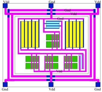
Area-Time Optimal Adder with Relative Placement Generator
 Area-Time Optimal Adder with Relative Placement Generator Abstract: This paper presents the design of a generator, for the production of area-time-optimal adders. A unique feature of this generator is
CPE/EE 427, CPE 527 VLSI Design I L18: Circuit Families. Outline
 CPE/EE 47, CPE 57 VLI Design I L8: Circuit Families Department of Electrical and Computer Engineering University of labama in Huntsville leksandar Milenkovic ( www.ece.uah.edu/~milenka ) www.ece.uah.edu/~milenka/cpe57-05f
Based on slides/material by. Topic 3-4. Combinational Logic. Outline. The CMOS Inverter: A First Glance
 ased on slides/material by Topic 3 J. Rabaey http://bwrc.eecs.berkeley.edu/lasses/icook/instructors.html Digital Integrated ircuits: Design Perspective, Prentice Hall D. Harris http://www.cmosvlsi.com/coursematerials.html
EE141- Spring 2004 Digital Integrated Circuits
 EE141- pring 2004 Digital Integrated ircuits Lecture 19 Dynamic Logic - Adders (that is wrap-up) 1 Administrative tuff Hw 6 due on Th No lab this week Midterm 2 next week Project 2 to be launched week
Adders allow computers to add numbers 2-bit ripple-carry adder
 Lecture 12 Logistics HW was due yesterday HW5 was out yesterday (due next Wednesday) Feedback: thank you! Things to work on: ig picture, ook chapters, Exam comments Last lecture dders Today Clarification
UNIT III Design of Combinational Logic Circuits. Department of Computer Science SRM UNIVERSITY
 UNIT III Design of ombinational Logic ircuits Department of omputer Science SRM UNIVERSITY Introduction to ombinational ircuits Logic circuits for digital systems may be ombinational Sequential combinational
Basic Gate Repertoire
 asic Gate Repertoire re we sure we have all the gates we need? Just how many two-input gates are there? ND OR NND NOR SURGE Hmmmm all of these have 2-inputs (no surprise) each with 4 combinations, giving
CMPEN 411 VLSI Digital Circuits Spring Lecture 21: Shifters, Decoders, Muxes
 CMPEN 411 VLSI Digital Circuits Spring 2011 Lecture 21: Shifters, Decoders, Muxes [Adapted from Rabaey s Digital Integrated Circuits, Second Edition, 2003 J. Rabaey, A. Chandrakasan, B. Nikolic] Sp11 CMPEN
EE115C Digital Electronic Circuits Homework #6
 Problem 1 Sizing of adder blocks Electrical Engineering Department Spring 2010 EE115C Digital Electronic Circuits Homework #6 Solution Figure 1: Mirror adder. Study the mirror adder cell (textbook, pages
MASSACHUSETTS INSTITUTE OF TECHNOLOGY Department of Electrical Engineering and Computer Sciences
 MASSACHUSETTS INSTITUTE OF TECHNOLOGY Department of Electrical Engineering and Computer Sciences Analysis and Design of Digital Integrated Circuits (6.374) - Fall 2003 Quiz #2 Prof. Anantha Chandrakasan
CSE140: Components and Design Techniques for Digital Systems. Decoders, adders, comparators, multipliers and other ALU elements. Tajana Simunic Rosing
 CSE4: Components and Design Techniques for Digital Systems Decoders, adders, comparators, multipliers and other ALU elements Tajana Simunic Rosing Mux, Demux Encoder, Decoder 2 Transmission Gate: Mux/Tristate
CSE370 HW3 Solutions (Winter 2010)
") CSE370 HW3 Solutions (Winter 2010) 1. CL2e, 4.9 We are asked to implement the function f(a,,c,,e) = A + C + + + CE using the smallest possible multiplexer. We can t use any extra gates or the complement
CSE370 HW3 Solutions (Winter 2010) 1. CL2e, 4.9 We are asked to implement the function f(a,,c,,e) = A + C + + + CE using the smallest possible multiplexer. We can t use any extra gates or the complement
C.K. Ken Yang UCLA Courtesy of MAH EE 215B
 Decoders: Logical Effort Applied C.K. Ken Yang UCLA yang@ee.ucla.edu Courtesy of MAH 1 Overview Reading Rabaey 6.2.2 (Ratio-ed logic) W&H 6.2.2 Overview We have now gone through the basics of decoders,
Dynamic Combinational Circuits. Dynamic Logic
 Dynamic Combinational Circuits Dynamic circuits Charge sharing, charge redistribution Domino logic np-cmos (zipper CMOS) Krish Chakrabarty 1 Dynamic Logic Dynamic gates use a clocked pmos pullup Two modes:
Lecture 8: Combinational Circuit Design
 Lecture 8: Combinational Circuit Design Mark McDermott Electrical and Computer Engineering The University of Texas at ustin 9/5/8 Verilog to Gates module mux(input s, d0, d, output y); assign y = s? d
Lecture 4: Implementing Logic in CMOS
 Lecture 4: Implementing Logic in CMOS Mark Mcermott Electrical and Computer Engineering The University of Texas at ustin Review of emorgan s Theorem Recall that: () = + and = ( + ) (+) = and + = ( ) ()
CPE/EE 427, CPE 527 VLSI Design I L07: CMOS Logic Gates, Pass Transistor Logic. Review: CMOS Circuit Styles
 PE/EE 427, PE 527 VLI esign I L07: MO Logic Gates, Pass Transistor Logic epartment of Electrical and omputer Engineering University of labama in Huntsville leksandar Milenkovic ( www.ece.uah.edu/~milenka
CMPEN 411 VLSI Digital Circuits Spring 2011 Lecture 07: Pass Transistor Logic
 CMPEN 411 VLSI Digital Circuits Spring 2011 Lecture 07: Pass Transistor Logic [dapted from Rabaey s Digital Integrated Circuits, Second Edition, 2003 J. Rabaey,. Chandrakasan,. Nikolic] Sp11 CMPEN 411
Slide Set 6. for ENEL 353 Fall Steve Norman, PhD, PEng. Electrical & Computer Engineering Schulich School of Engineering University of Calgary
 Slide Set 6 for ENEL 353 Fall 2017 Steve Norman, PhD, PEng Electrical & Computer Engineering Schulich School of Engineering University of Calgary Fall Term, 2017 SN s ENEL 353 Fall 2017 Slide Set 6 slide
Datapath Component Tradeoffs
 Datapath Component Tradeoffs Faster Adders Previously we studied the ripple-carry adder. This design isn t feasible for larger adders due to the ripple delay. ʽ There are several methods that we could
9. Datapath Design. Jacob Abraham. Department of Electrical and Computer Engineering The University of Texas at Austin VLSI Design Fall 2017
 9. Datapath Design Jacob Abraham Department of Electrical and Computer Engineering The University of Texas at Austin VLSI Design Fall 2017 October 2, 2017 ECE Department, University of Texas at Austin
Prove that if not fat and not triangle necessarily means not green then green must be fat or triangle (or both).
.") hapter : oolean lgebra.) Definition of oolean lgebra The oolean algebra is named after George ool who developed this algebra (854) in order to analyze logical problems. n example to such problem is: Prove
hapter : oolean lgebra.) Definition of oolean lgebra The oolean algebra is named after George ool who developed this algebra (854) in order to analyze logical problems. n example to such problem is: Prove
Arithmetic Circuits How to add and subtract using combinational logic Setting flags Adding faster
 rithmetic Circuits Didn t I learn how to do addition in second grade? UNC courses aren t what they used to be... 01011 +00101 10000 Finally; time to build some serious functional blocks We ll need a lot
Miscellaneous Lecture topics. Mary Jane Irwin [Adapted from Rabaey s Digital Integrated Circuits, 2002, J. Rabaey et al.]
![Miscellaneous Lecture topics. Mary Jane Irwin [Adapted from Rabaey s Digital Integrated Circuits, 2002, J. Rabaey et al.]](/thumbs/81/84503671.jpg "Miscellaneous Lecture topics. Mary Jane Irwin [Adapted from Rabaey s Digital Integrated Circuits, 2002, J. Rabaey et al.]") Miscellaneous Lecture topics Mary Jane Irwin [dapted from Rabaey s Digital Integrated Circuits, 2002, J. Rabaey et al.] MOS Switches MOS transistors can be viewed as simple switches. In an N-Switch, the
Miscellaneous Lecture topics Mary Jane Irwin [dapted from Rabaey s Digital Integrated Circuits, 2002, J. Rabaey et al.] MOS Switches MOS transistors can be viewed as simple switches. In an N-Switch, the
8. Design Tradeoffs x Computation Structures Part 1 Digital Circuits. Copyright 2015 MIT EECS
 8. Design Tradeoffs 6.004x Computation Structures Part 1 Digital Circuits Copyright 2015 MIT EECS 6.004 Computation Structures L08: Design Tradeoffs, Slide #1 There are a large number of implementations
8. Design Tradeoffs x Computation Structures Part 1 Digital Circuits. Copyright 2015 MIT EECS
 8. Design Tradeoffs 6.004x Computation Structures Part 1 Digital Circuits Copyright 2015 MIT EECS 6.004 Computation Structures L08: Design Tradeoffs, Slide #1 There are a large number of implementations
L8/9: Arithmetic Structures
 L8/9: Arithmetic Structures Acknowledgements: Materials in this lecture are courtesy of the following sources and are used with permission. Rex Min Kevin Atkinson Prof. Randy Katz (Unified Microelectronics
Digital Integrated Circuits A Design Perspective
 Digital Integrated Circuits Design Perspective Jan M. Rabaey nantha Chandrakasan orivoje Nikolić Designing Combinational Logic Circuits November 2002. 1 Combinational vs. Sequential Logic In Combinational
Digital EE141 Integrated Circuits 2nd Combinational Circuits
 Digital Integrated Circuits Designing i Combinational Logic Circuits 1 Combinational vs. Sequential Logic 2 Static CMOS Circuit t every point in time (except during the switching transients) each gate
EEC 216 Lecture #3: Power Estimation, Interconnect, & Architecture. Rajeevan Amirtharajah University of California, Davis
 EEC 216 Lecture #3: Power Estimation, Interconnect, & Architecture Rajeevan Amirtharajah University of California, Davis Outline Announcements Review: PDP, EDP, Intersignal Correlations, Glitching, Top
Announcements. EE141-Spring 2007 Digital Integrated Circuits. CMOS SRAM Analysis (Read/Write) Class Material. Layout. Read Static Noise Margin
 Class Material. Layout. Read Static Noise Margin") Vo l ta ge ri s e [ V] EE-Spring 7 Digital Integrated ircuits Lecture SRM Project Launch nnouncements No new labs next week and week after Use labs to work on project Homework #6 due Fr. pm Project updated
Vo l ta ge ri s e [ V] EE-Spring 7 Digital Integrated ircuits Lecture SRM Project Launch nnouncements No new labs next week and week after Use labs to work on project Homework #6 due Fr. pm Project updated
Digital Integrated Circuits A Design Perspective
 Digital Integrated Circuits Design Perspective Jan M. Rabaey nantha Chandrakasan orivoje Nikolić Designing Combinational Logic Circuits November 2002. 1 Views / bstractions / Hierarchies ehavioral Structural
Binary addition by hand. Adding two bits
 Chapter 3 Arithmetic is the most basic thing you can do with a computer We focus on addition, subtraction, multiplication and arithmetic-logic units, or ALUs, which are the heart of CPUs. ALU design Bit
S No. Questions Bloom s Taxonomy Level UNIT-I
 GROUP-A (SHORT ANSWER QUESTIONS) S No. Questions Bloom s UNIT-I 1 Define oxidation & Classify different types of oxidation Remember 1 2 Explain about Ion implantation Understand 1 3 Describe lithography
CMOS logic gates. João Canas Ferreira. March University of Porto Faculty of Engineering
 CMOS logic gates João Canas Ferreira University of Porto Faculty of Engineering March 2016 Topics 1 General structure 2 General properties 3 Cell layout João Canas Ferreira (FEUP) CMOS logic gates March
SRC Language Conventions. Class 6: Intro to SRC Simulator Register Transfers and Logic Circuits. SRC Simulator Demo. cond_br.asm.
 Fall 2006 S333: omputer rchitecture University of Virginia omputer Science Michele o SR Language onventions lass 6: Intro to SR Simulator Register Transfers and Logic ircuits hapter 2, ppendix.5 2 SR Simulator
Logic Synthesis and Verification
 Logic Synthesis and Verification Jie-Hong Roland Jiang 江介宏 Department of Electrical Engineering National Taiwan University Fall Timing Analysis & Optimization Reading: Logic Synthesis in a Nutshell Sections
Optimum Prefix Adders in a Comprehensive Area, Timing and Power Design Space
 Optimum Prefix Adders in a Comprehensive Area, Timing and Power Design Space Jianhua Liu, Yi Zhu, Haikun Zhu, John Lillis 2, Chung-Kuan Cheng Department of Computer Science and Engineering University of
ESE 570: Digital Integrated Circuits and VLSI Fundamentals
 ESE 570: Digital Integrated Circuits and VLSI Fundamentals Lec 18: March 27, 2018 Dynamic Logic, Charge Injection Lecture Outline! Sequential MOS Logic " D-Latch " Timing Constraints! Dynamic Logic " Domino
Appendix A: Digital Logic. Principles of Computer Architecture. Principles of Computer Architecture by M. Murdocca and V. Heuring
 - Principles of Computer rchitecture Miles Murdocca and Vincent Heuring 999 M. Murdocca and V. Heuring -2 Chapter Contents. Introduction.2 Combinational Logic.3 Truth Tables.4 Logic Gates.5 Properties
UNIT 8A Computer Circuitry: Layers of Abstraction. Boolean Logic & Truth Tables
 UNIT 8 Computer Circuitry: Layers of bstraction 1 oolean Logic & Truth Tables Computer circuitry works based on oolean logic: operations on true (1) and false (0) values. ( ND ) (Ruby: && ) 0 0 0 0 0 1
Hardware Design I Chap. 4 Representative combinational logic
 Hardware Design I Chap. 4 Representative combinational logic E-mail: shimada@is.naist.jp Already optimized circuits There are many optimized circuits which are well used You can reduce your design workload
Topics. Dynamic CMOS Sequential Design Memory and Control. John A. Chandy Dept. of Electrical and Computer Engineering University of Connecticut
 Topics Dynamic CMOS Sequential Design Memory and Control Dynamic CMOS In static circuits at every point in time (except when switching) the output is connected to either GND or V DD via a low resistance
Static CMOS Circuits. Example 1
 Static CMOS Circuits Conventional (ratio-less) static CMOS Covered so far Ratio-ed logic (depletion load, pseudo nmos) Pass transistor logic ECE 261 Krish Chakrabarty 1 Example 1 module mux(input s, d0,
Lecture 6: Logical Effort
 Lecture 6: Logical Effort Outline Logical Effort Delay in a Logic Gate Multistage Logic Networks Choosing the Best Number of Stages Example Summary Introduction Chip designers face a bewildering array
Chapter 5 CMOS Logic Gate Design
 Chapter 5 CMOS Logic Gate Design Section 5. -To achieve correct operation of integrated logic gates, we need to satisfy 1. Functional specification. Temporal (timing) constraint. (1) In CMOS, incorrect
Logic Synthesis. Late Policies. Wire Gauge. Schematics & Wiring
 Late Policies Logic Synthesis Primitive logic gates, universal gates Truth tables and sum-of-products Logic simplification Karnaugh Maps, Quine-Mcluskey General implementation techniques: muxes and look-up
ALUs and Data Paths. Subtitle: How to design the data path of a processor. 1/8/ L3 Data Path Design Copyright Joanne DeGroat, ECE, OSU 1
 ALUs and Data Paths Subtitle: How to design the data path of a processor. Copyright 2006 - Joanne DeGroat, ECE, OSU 1 Lecture overview General Data Path of a multifunction ALU Copyright 2006 - Joanne DeGroat,
Pass-Transistor Logic
 -all 26 Digital tegrated ircuits nnouncements No new homework this week roject phase one due on Monday Midterm 2 next Thursday Review session on Tuesday Lecture 8 Logic Dynamic Logic EE4 EE4 2 lass Material
ECE429 Introduction to VLSI Design
 ECE429 Introduction to VLSI Design Lecture 5: LOGICAL EFFORT Erdal Oruklu Illinois Institute of Technology Some of these slides have been adapted from the slides provided by David Harris, Harvey Mudd College
EE 447 VLSI Design. Lecture 5: Logical Effort
 EE 447 VLSI Design Lecture 5: Logical Effort Outline Introduction Delay in a Logic Gate Multistage Logic Networks Choosing the Best Number of Stages Example Summary EE 4475: VLSI Logical Design Effort
Ch 4. Combinational Logic Technologies. IV - Combinational Logic Technologies Contemporary Logic Design 1
 h 4. ombinational Logic Technologies Technologies ontemporary Logic Design 1 History - From Switches to Integrated ircuits The underlying implementation technologies for digital systems Technologies ontemporary
Chapter 2. Introduction. Chapter 2 :: Topics. Circuits. Nodes. Circuit elements. Introduction
 hapter 2 Introduction igital esign and omputer rchitecture, 2 nd Edition avid Money Harris and Sarah L. Harris logic circuit is composed of: Inputs Outputs Functional specification Timing specification
Arithmetic Circuits-2
 Arithmetic Circuits-2 Multipliers Array multipliers Shifters Barrel shifter Logarithmic shifter ECE 261 Krish Chakrabarty 1 Binary Multiplication M-1 X = X i 2 i i=0 Multiplicand N-1 Y = Y i 2 i i=0 Multiplier
COMBINATIONAL LOGIC. Combinational Logic
 COMINTIONL LOGIC Overview Static CMOS Conventional Static CMOS Logic Ratioed Logic Pass Transistor/Transmission Gate Logic Dynamic CMOS Logic Domino np-cmos Combinational vs. Sequential Logic In Logic
Logic. Basic Logic Functions. Switches in series (AND) Truth Tables. Switches in Parallel (OR) Alternative view for OR
 Truth Tables. Switches in Parallel (OR) Alternative view for OR") TOPIS: Logic Logic Expressions Logic Gates Simplifying Logic Expressions Sequential Logic (Logic with a Memory) George oole (85-864), English mathematician, oolean logic used in digital computers since
TOPIS: Logic Logic Expressions Logic Gates Simplifying Logic Expressions Sequential Logic (Logic with a Memory) George oole (85-864), English mathematician, oolean logic used in digital computers since
CprE 281: Digital Logic
 CprE 281: Digital Logic Instructor: Alexander Stoytchev http://www.ece.iastate.edu/~alexs/classes/ Fast Adders CprE 281: Digital Logic Iowa State University, Ames, IA Copyright Alexander Stoytchev HW5
9/18/2008 GMU, ECE 680 Physical VLSI Design
 ECE680: Physical VLSI Design Chapter III CMOS Device, Inverter, Combinational circuit Logic and Layout Part 3 Combinational Logic Gates (textbook chapter 6) 9/18/2008 GMU, ECE 680 Physical VLSI Design
Possible logic functions of two variables
 ombinational logic asic logic oolean algebra, proofs by re-writing, proofs by perfect induction logic functions, truth tables, and switches NOT, ND, OR, NND, NOR, OR,..., minimal set Logic realization