Edited By : Engr. Muhammad Muizz bin Mohd Nawawi
|
|
|
- Kathlyn Jordan
- 5 years ago
- Views:
Transcription


1 Edited By : Engr. Muhammad Muizz bin Mohd Nawawi
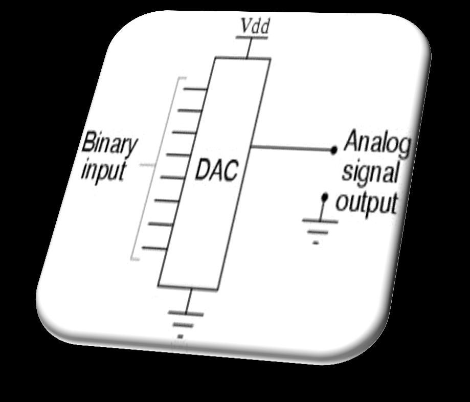
2 In an electronic circuit, a combination of high voltage (+5V) and low voltage (0V) is usually used to represent a binary number. For example, a binary number 1010 is represented by Weighting Binary Digit State +5V 0V +5V 0V DACs are electronic circuits that convert digital, (usually binary) signals (for example, ) to analog electrical quantities (usually voltage) directly related to the digitally encoded input number.

3


4 DIGITAL TO ANALOGUE CONVETE


5
6 egister DACs are used in many other applications, such as voice synthesizers, automatic test system, and process control actuator. In addition, they allow computers to communicate with the real (analog) world. Input Binary Number Voltage Switch esistive Summing Network Amplifier Analog Voltage Output

7 Audio Video
8
9 Binary Weighted esistor Ii f = V o MSB LSB -V EF 10
10 Binary Weighted esistor Ii f = Most Significant Bit V o Least Significant Bit -V EF 11
11 Binary Weighted esistor Most Significant Bit SET CLEAED -V EF Least Significant Bit ( ) 2 = ( 15 ) 10 12
12 Binary Weighted esistor Weighted esistors based on bit Ii f = educes current by a factor of 2 for each bit MSB V o LSB -V EF 13
13 14 esult: B i = Value of Bit i B B B B V I EF B B B B V I V EF f OUT Binary Weighted esistor
14 Binary Weighted esistor More Generally: V OUT B i = Value of Bit i n = Number of Bits B i VEF n 2 i V Digital EF 1 Value esolution 15
15 The circuit in above figure is a digital to analog converter circuit of resistors 4-bit binary weights. We can calculate the resistor values using the weight of binary numbers. For example, the most high-value resistor (150 kω = 1) is a digital input resistor, the smallest bit (least significant bit), and the values of the other resistor are: 2 = 1 = 150K = 75 kω Bit 21 3 = 1 = 150K = 1 = 150K = 37.5 kω Bit 2 2 = kω Bit 2 3
16 Now we will analyze the circuit to get the output, Vout for a number of digital input. i. Binary input = = 150 kω, F = 20 kω, The gain of the voltage (AV) = F / 1 = Vout = Vref x AV = 3 V X = 0.4V ii. Binary input = = 75 kω, 3 = 37.5 kω, T = (2 3 partially parallel) = 25 kω. AV = 20 kω /25 kω = 0.8, Vout = Vref x AV = 3 V X 0.8 = 2.4V or in = Vout = Vref and F resistance. Vout can found by substituting the resistance values of the total amount of resistance when certain binary input. In summary we can see the resulting output is shown in Table below.
17 Table 1 Decimal Binary Input D C B A V out (V)

18 This circuit is different from binary up a resistor DAC circuit because it only uses two resistor values, and 2. Disadvantage that we can see is too much of the resistor to be provided. For example, if 12-bit DAC with resistor value MSB (most significant bit), then it is 1kΩ resistor will exceed 2MΩ LSB.
19 One method of analyzing this circuit is to find a resolution for this circuit. The resolution [full-scale resolution] for this circuit is the Vref / 3 ie by setting input 012 = 110. Full scale output of the circuit is by setting the input will produce 112 = 310 = Vout. Then the general expression for the circuit is Vout = where n = number of bits and B in = digital input converted to decimal numbers.
20 a) From figure a below, when input 01 2 = 1 10, Vout = b) The input 10 2, the circuit is as figure b From figure b, when input 10 2 = 2 10, Vout = c) The input 11 2, the circuit is as figure c. From figure c, when input 11 2 = 3 10, Vout = We can get the general equation for output as: V ref 2 3V 4 ref f f V ref 4 f V 0ut = V 00 + V 01 + V 10 + V 11 = 0 + V ref f V 0ut = V ref 4 f + V ref 2 f + 3V 4 ref f In conclusion, from what we have to prove from the analysis on the circuit, the output Vout = V ref n 2 converted to decimal. f B in,where n = number of bits and B in = binary input that has been
21 Masukan D C B A Jadual 5.2 keluaran,v OUT V OUT = V 2 ref n f B 5 16 in = B in B 4 in 2 5
22 Defined as the smallest change achieved in the analog output as a result of changes in digital input. esolution can be expressed in two cases, either the voltage or Ampere and also percent also known as the step size. Maximum output voltage.


23
24 Digital to analog converter 10-bit with step size 10 mv. Search for full-scale voltage and percent resolution.


25
26
27

28
29


30 Digital to Analog Converters -Common Applications -Digital Audio 1 2 3


31 Digital to Analog Converters -Common Applications -Function Generators 1 2


32 Digital to Analog Converters -Common Applications -Motor Controllers 1 2 3


33
PARALLEL DIGITAL-ANALOG CONVERTERS
 CMOS Analog IC Design Page 10.2-1 10.2 - PARALLEL DIGITAL-ANALOG CONVERTERS CLASSIFICATION OF DIGITAL-ANALOG CONVERTERS CMOS Analog IC Design Page 10.2-2 CURRENT SCALING DIGITAL-ANALOG CONVERTERS GENERAL
EE 435. Lecture 38. DAC Design Current Steering DACs Charge Redistribution DACs ADC Design
 EE 435 Lecture 38 DAC Design Current Steering DACs Charge edistribution DACs ADC Design eview from last lecture Current Steering DACs X N Binary to Thermometer ndecoder (all ON) S S N- S N V EF F nherently
Analog to Digital Conversion
 Analog to Digital Conversion ATmega Block Diagram Analog to Digital Converter Sample and Hold SA Converter Internal Bandgap eference 2 tj Analog to Digital Conversion Most of the real world is analog temperature,
EXTENDING THE RESOLUTION OF PARALLEL DIGITAL-ANALOG CONVERTERS
 CMOS Analog IC Design Page 10.3-1 10.3 - EXTENDING THE RESOLUTION OF PARALLEL DIGITAL-ANALOG CONVERTERS TECHNIQUE: Divide the total resolution N into k smaller sub-dacs each with a resolution of N k. Result:
EE100Su08 Lecture #9 (July 16 th 2008)
") EE100Su08 Lecture #9 (July 16 th 2008) Outline HW #1s and Midterm #1 returned today Midterm #1 notes HW #1 and Midterm #1 regrade deadline: Wednesday, July 23 rd 2008, 5:00 pm PST. Procedure: HW #1: Bart
EE100Su08 Lecture #9 (July 16 th 2008) Outline HW #1s and Midterm #1 returned today Midterm #1 notes HW #1 and Midterm #1 regrade deadline: Wednesday, July 23 rd 2008, 5:00 pm PST. Procedure: HW #1: Bart
D/A Converters. D/A Examples
 D/A architecture examples Unit element Binary weighted Static performance Component matching Architectures Unit element Binary weighted Segmented Dynamic element matching Dynamic performance Glitches Reconstruction
The equivalent model of a certain op amp is shown in the figure given below, where R 1 = 2.8 MΩ, R 2 = 39 Ω, and A =
 The equivalent model of a certain op amp is shown in the figure given below, where R 1 = 2.8 MΩ, R 2 = 39 Ω, and A = 10 10 4. Section Break Difficulty: Easy Learning Objective: Understand how real operational
Digital Electronic Meters
 Digital Electronic Meters EIE 240 Electrical and Electronic Measurement May 1, 2015 1 Digital Signal Binary or two stages: 0 (Low voltage 0-3 V) 1 (High voltage 4-5 V) Binary digit is called bit. Group
Measurement and Instrumentation. Sampling, Digital Devices, and Data Acquisition
 2141-375 Measurement and Instrumentation Sampling, Digital Devices, and Data Acquisition Basic Data Acquisition System Analog Form Analog Form Digital Form Display Physical varialble Sensor Signal conditioning
Operational Amplifiers
 Operational Amplifiers A Linear IC circuit Operational Amplifier (op-amp) An op-amp is a high-gain amplifier that has high input impedance and low output impedance. An ideal op-amp has infinite gain and
Nyquist-Rate D/A Converters. D/A Converter Basics.
 Nyquist-Rate D/A Converters David Johns and Ken Martin (johns@eecg.toronto.edu) (martin@eecg.toronto.edu) slide 1 of 20 D/A Converter Basics. B in D/A is a digital signal (or word), B in b i B in = 2 1
Designing Information Devices and Systems I Fall 2018 Lecture Notes Note Introduction: Op-amps in Negative Feedback
 EECS 16A Designing Information Devices and Systems I Fall 2018 Lecture Notes Note 18 18.1 Introduction: Op-amps in Negative Feedback In the last note, we saw that can use an op-amp as a comparator. However,
Week No. 06: Numbering Systems
 Week No. 06: Numbering Systems Numbering System: A numbering system defined as A set of values used to represent quantity. OR A number system is a term used for a set of different symbols or digits, which
Digital Signal 2 N Most Significant Bit (MSB) Least. Bit (LSB)
 Least. Bit (LSB)") 1 Digital Signal Binary or two stages: 0 (Low voltage 0-3 V) 1 (High voltage 4-5 V) Binary digit is called bit. Group of bits is called word. 8-bit group is called byte. For N-bit base-2 number = 2 N levels
1 Digital Signal Binary or two stages: 0 (Low voltage 0-3 V) 1 (High voltage 4-5 V) Binary digit is called bit. Group of bits is called word. 8-bit group is called byte. For N-bit base-2 number = 2 N levels
Lecture 340 Characterization of DACs and Current Scaling DACs (5/1/10) Page 340-1
 Page 340-1") Lecture 34 Characterization of DACs and Current Scaling DACs (5//) Page 34 LECTURE 34 CHARACTERZATON OF DACS AND CURRENT SCALNG DACS LECTURE ORGANZATON Outline ntroduction Static characterization of DACs
Lecture 34 Characterization of DACs and Current Scaling DACs (5//) Page 34 LECTURE 34 CHARACTERZATON OF DACS AND CURRENT SCALNG DACS LECTURE ORGANZATON Outline ntroduction Static characterization of DACs
In this lecture, we will consider how to analyse an electrical circuit by applying KVL and KCL. As a result, we can predict the voltages and currents
 In this lecture, we will consider how to analyse an electrical circuit by applying KVL and KCL. As a result, we can predict the voltages and currents around an electrical circuit. This is a short lecture,
EE 505 Lecture 8. Clock Jitter Statistical Circuit Modeling
 EE 505 Lecture 8 Clock Jitter Statistical Circuit Modeling Spectral Characterization of Data Converters Distortion Analysis Time Quantization Effects of DACs of ADCs Amplitude Quantization Effects of DACs
Prelaboratory. EE223 Laboratory #1 Digital to Analog Converter
 EE223 Laboratory #1 Digital to Analog Converter Objectives: 1) Learn how superposition and Thevenin conversions are used to analyze practical circuits 2) Become familiar with ground bus and power bus notation
EE 521: Instrumentation and Measurements
 Aly El-Osery Electrical Engineering Department, New Mexico Tech Socorro, New Mexico, USA September 23, 2009 1 / 18 1 Sampling 2 Quantization 3 Digital-to-Analog Converter 4 Analog-to-Digital Converter
Solved Problems. Electric Circuits & Components. 1-1 Write the KVL equation for the circuit shown.
 Solved Problems Electric Circuits & Components 1-1 Write the KVL equation for the circuit shown. 1-2 Write the KCL equation for the principal node shown. 1-2A In the DC circuit given in Fig. 1, find (i)
A Gray Code Based Time-to-Digital Converter Architecture and its FPGA Implementation
 A Gray Code Based Time-to-Digital Converter Architecture and its FPGA Implementation Congbing Li Haruo Kobayashi Gunma University Gunma University Kobayashi Lab Outline Research Objective & Background
Design Engineering MEng EXAMINATIONS 2016
 IMPERIAL COLLEGE LONDON Design Engineering MEng EXAMINATIONS 2016 For Internal Students of the Imperial College of Science, Technology and Medicine This paper is also taken for the relevant examination
Digital to Analog Converters I
 Advanced Analog Building Blocks 2 Digital to Analog Converters I Albert Comerma (PI) (comerma@physi.uni-heidelberg.de) Course web WiSe 2017 DAC parameters DACs parameters DACs non ideal effects DACs performance
per chip (approx) 1 SSI (Small Scale Integration) Up to 99
 1 SSI (Small Scale Integration) Up to 99") Q.2 a. Classify the integration technology as per the scale of integration. Explain in brief the various steps involved in fabrication of monolithic IC. Scales of Integration (Basic) Various steps involved
Q.2 a. Classify the integration technology as per the scale of integration. Explain in brief the various steps involved in fabrication of monolithic IC. Scales of Integration (Basic) Various steps involved
Schedule. ECEN 301 Discussion #25 Final Review 1. Date Day Class No. 1 Dec Mon 25 Final Review. Title Chapters HW Due date. Lab Due date.
 Schedule Date Day Class No. Dec Mon 25 Final Review 2 Dec Tue 3 Dec Wed 26 Final Review Title Chapters HW Due date Lab Due date LAB 8 Exam 4 Dec Thu 5 Dec Fri Recitation HW 6 Dec Sat 7 Dec Sun 8 Dec Mon
Delta & Y Configurations, Principles of Superposition, Resistor Voltage Divider Designs
 BME/ISE 3511 Bioelectronics - Test Three Course Notes Fall 2016 Delta & Y Configurations, Principles of Superposition, esistor Voltage Divider Designs Use following techniques to solve for current through
Digital Circuits, Binary Numbering, and Logic Gates Cornerstone Electronics Technology and Robotics II
 Digital Circuits, Binary Numbering, and Logic Gates Cornerstone Electronics Technology and Robotics II Administration: o Prayer Electricity and Electronics, Section 20.1, Digital Fundamentals: o Fundamentals:
Chapter 5 Objectives
 Chapter 5 Engr228 Circuit Analysis Dr Curtis Nelson Chapter 5 Objectives State and apply the property of linearity State and apply the property of superposition Investigate source transformations Define
Lecture 10, ATIK. Data converters 3
 Lecture, ATIK Data converters 3 What did we do last time? A quick glance at sigma-delta modulators Understanding how the noise is shaped to higher frequencies DACs A case study of the current-steering
Signal types. Signal characteristics: RMS, power, db Probability Density Function (PDF). Analogue-to-Digital Conversion (ADC).
. Analogue-to-Digital Conversion (ADC).") Signal types. Signal characteristics:, power, db Probability Density Function (PDF). Analogue-to-Digital Conversion (ADC). Signal types Stationary (average properties don t vary with time) Deterministic
Signal types. Signal characteristics:, power, db Probability Density Function (PDF). Analogue-to-Digital Conversion (ADC). Signal types Stationary (average properties don t vary with time) Deterministic
Kirchhoff's Laws and Circuit Analysis (EC 2)
") Kirchhoff's Laws and Circuit Analysis (EC ) Circuit analysis: solving for I and V at each element Linear circuits: involve resistors, capacitors, inductors Initial analysis uses only resistors Power sources,
Kirchhoff's Laws and Circuit Analysis (EC ) Circuit analysis: solving for I and V at each element Linear circuits: involve resistors, capacitors, inductors Initial analysis uses only resistors Power sources,
A novel Capacitor Array based Digital to Analog Converter
 Chapter 4 A novel Capacitor Array based Digital to Analog Converter We present a novel capacitor array digital to analog converter(dac architecture. This DAC architecture replaces the large MSB (Most Significant
EE 321 Analog Electronics, Fall 2013 Homework #3 solution
 EE 32 Analog Electronics, Fall 203 Homework #3 solution 2.47. (a) Use superposition to show that the output of the circuit in Fig. P2.47 is given by + [ Rf v N + R f v N2 +... + R ] f v Nn R N R N2 R [
MAHARASHTRA STATE BOARD OF TECHNICAL EDUCATION (Autonomous) (ISO/IEC Certified) State any two Boolean laws. (Any 2 laws 1 mark each)
 (ISO/IEC Certified) State any two Boolean laws. (Any 2 laws 1 mark each)") Subject Code: 17333 Model Answer Page 1/ 27 Important Instructions to examiners: 1) The answers should be examined by key words and not as word-to-word as given in the model answer scheme. 2) The model
Subject Code: 17333 Model Answer Page 1/ 27 Important Instructions to examiners: 1) The answers should be examined by key words and not as word-to-word as given in the model answer scheme. 2) The model
SPS Presents: A Cosmic Lunch!
 SPS Presents: A Cosmic Lunch! Who: Dr. Brown will be speaking about Evolution of the Elements: from Periodic table to Standard Model and Beyond! When: October 7 th at am Where: CP 79 (by the front office)
Analog Digital Sampling & Discrete Time Discrete Values & Noise Digital-to-Analog Conversion Analog-to-Digital Conversion
 Analog Digital Sampling & Discrete Time Discrete Values & Noise Digital-to-Analog Conversion Analog-to-Digital Conversion 6.082 Fall 2006 Analog Digital, Slide Plan: Mixed Signal Architecture volts bits
ECE 1311: Electric Circuits. Chapter 2: Basic laws
 ECE 1311: Electric Circuits Chapter 2: Basic laws Basic Law Overview Ideal sources series and parallel Ohm s law Definitions open circuits, short circuits, conductance, nodes, branches, loops Kirchhoff's
EECE 2510 Circuits and Signals, Biomedical Applications Final Exam Section 3. Name:
 EECE 2510 Circuits and Signals, Biomedical Applications Final Exam Section 3 Instructions: Closed book, closed notes; Computers and cell phones are not allowed Scientific calculators are allowed Complete
Midterm 1 Announcements
 Midterm Announcements eiew session: 5-8pm TONIGHT 77 Cory Midterm : :30-pm on Tuesday, July Dwelle 45. Material coered HW-3 Attend only your second lab slot this wee EE40 Summer 005: Lecture 9 Instructor:
Electrical Circuits. Winchester College Physics. makptb. c D. Common Time man. 3rd year Revision Test
 Name... Set... Don.... manner~ man makptb Winchester College Physics 3rd year Revision Test Electrical Circuits Common Time 2011 Mark multiple choice answers with a cross (X) using the box below. I A B
5-BIT PROGRAMMABLE VOLTAGE REFERENCE P R O D U C T I O N D ATA S H E E T
 LIN DOC #: 10 T HE I N F I N I T E P O W E R OF I N N O V A TION DESCRIPTION KEY FEATURES The is a complete precision reference and voltage monitor circuit for the Intel Pentium Pro Processor and other
MECHATRONICS ENGINEERING TECHNOLOGY. Modeling a Servo Motor System
 Modeling a Servo Motor System Definitions Motor: A device that receives a continuous (Analog) signal and operates continuously in time. Digital Controller: Discretizes the amplitude of the signal and also
Data Converter Fundamentals
 Data Converter Fundamentals David Johns and Ken Martin (johns@eecg.toronto.edu) (martin@eecg.toronto.edu) slide 1 of 33 Introduction Two main types of converters Nyquist-Rate Converters Generate output
CMOS Low Cost, 10-Bit Multiplying DAC AD7533
 CMOS Low Cost, 0-Bit Multiplying DAC FEATUES Low cost 0-bit DAC Low cost AD750 replacement Linearity: ½,, or Low power dissipation Full -quadrant multiplying DAC CMOS/TTL direct interface Latch free (protection
CMOS Low Cost 10-Bit Multiplying DAC AD7533
 CMOS Low Cost 0-Bit Multiplying DAC FEATUES Low cost 0-bit DAC Low cost AD750 replacement Linearity: ½,, or Low power dissipation Full four-quadrant multiplying DAC CMOS/TTL direct interface Latch free
ESE319 Introduction to Microelectronics. Output Stages
 Output Stages Power amplifier classification Class A amplifier circuits Class A Power conversion efficiency Class B amplifier circuits Class B Power conversion efficiency Class AB amplifier circuits Class
Nyquist-Rate A/D Converters
 IsLab Analog Integrated ircuit Design AD-51 Nyquist-ate A/D onverters כ Kyungpook National University IsLab Analog Integrated ircuit Design AD-1 Nyquist-ate MOS A/D onverters Nyquist-rate : oversampling
ECE260: Fundamentals of Computer Engineering
 Data Representation & 2 s Complement James Moscola Dept. of Engineering & Computer Science York College of Pennsylvania Based on Computer Organization and Design, 5th Edition by Patterson & Hennessy Data
Identify the specified numbers by circling. 1) The integers in the following list: 8 16, 8, -10, 0, 9, - 9
 The integers in the following list: 8 16, 8, -10, 0, 9, - 9") MAT 105-01C TEST 1 REVIEW NAME Identify the specified numbers by circling. 1) The integers in the following list: 8 16, 8, -10, 0, 9, - 9, 5.5, 16 8 2) The rational numbers in the following list: 0 14,
MAT 105-01C TEST 1 REVIEW NAME Identify the specified numbers by circling. 1) The integers in the following list: 8 16, 8, -10, 0, 9, - 9, 5.5, 16 8 2) The rational numbers in the following list: 0 14,
MAHARASHTRA STATE BOARD OF TECHNICAL EDUCATION (Autonomous) (ISO/IEC Certified) SUMMER 14 EXAMINATION Model Answer
 (ISO/IEC Certified) SUMMER 14 EXAMINATION Model Answer") MAHARASHTRA STATE BOARD OF TECHNICAL EDUCATION (Autonomous) (ISO/IEC 27001 2005 Certified) SUMMER 14 EXAMINATION Model Answer Subject Code : 17320 Page No: 1/34 Important Instructions to examiners: 1)
MAHARASHTRA STATE BOARD OF TECHNICAL EDUCATION (Autonomous) (ISO/IEC 27001 2005 Certified) SUMMER 14 EXAMINATION Model Answer Subject Code : 17320 Page No: 1/34 Important Instructions to examiners: 1)
Unit 1 Lesson 1.2 Energy Sources
 Unit Lesson. Energy Sources ntroduction to Electricity 0 Electricity Movement of electrons nvisible force that provides light, heat, sound, motion... Elements he simplest form of matter Atoms Smallest
ELECTRONIC SYSTEMS. Basic operational amplifier circuits. Electronic Systems - C3 13/05/ DDC Storey 1
 Electronic Systems C3 3/05/2009 Politecnico di Torino ICT school Lesson C3 ELECTONIC SYSTEMS C OPEATIONAL AMPLIFIES C.3 Op Amp circuits» Application examples» Analysis of amplifier circuits» Single and
California University of Pennsylvania. Department of Applied Engineering & Technology. Electrical / Computer Engineering Technology
 California University of Pennsylvania Department of Applied Engineering & Technology Electrical / Computer Engineering Technology EET 215: Introduction to Instrumentations Lab No.7 Temperature Measurement
Introduction to Digital Logic Missouri S&T University CPE 2210 Number Systems
 Introduction to Digital Logic Missouri S&T University CPE 2210 Number Systems Egemen K. Çetinkaya Egemen K. Çetinkaya Department of Electrical & Computer Engineering Missouri University of Science and
Georgia Institute of Technology School of Electrical and Computer Engineering. Midterm-1 Exam (Solution)
") Georgia Institute of Technology School of Electrical and Computer Engineering Midterm-1 Exam (Solution) ECE-6414 Spring 2012 Friday, Feb. 17, 2012 Duration: 50min First name Solutions Last name Solutions
Georgia Institute of Technology School of Electrical and Computer Engineering Midterm-1 Exam (Solution) ECE-6414 Spring 2012 Friday, Feb. 17, 2012 Duration: 50min First name Solutions Last name Solutions
Electronics Capacitors
 Electronics Capacitors Wilfrid Laurier University October 9, 2015 Capacitor an electronic device which consists of two conductive plates separated by an insulator Capacitor an electronic device which consists
Voltage Dividers, Nodal, and Mesh Analysis
 Engr228 Lab #2 Voltage Dividers, Nodal, and Mesh Analysis Name Partner(s) Grade /10 Introduction This lab exercise is designed to further your understanding of the use of the lab equipment and to verify
SAMPLE EXAMINATION PAPER
 IMPERIAL COLLEGE LONDON Design Engineering MEng EXAMINATIONS 2016 For Internal Students of the Imperial College of Science, Technology and Medicine This paper is also taken for the relevant examination
Small Signal Model. S. Sivasubramani EE101- Small Signal - Diode
 Small Signal Model i v Small Signal Model i I D i d i D v d v D v V D Small Signal Model -Mathematical Analysis V D - DC value v d - ac signal v D - Total signal (DC ac signal) Diode current and voltage
EE 435. Lecture 36. Quantization Noise ENOB Absolute and Relative Accuracy DAC Design. The String DAC
 EE 435 Lecture 36 Quantization Noise ENOB Absolute and elative Accuracy DAC Design The String DAC . eview from last lecture. Quantization Noise in ADC ecall: If the random variable f is uniformly distributed
Lab 3 Revisited. Zener diodes IAP 2008 Lecture 4 1
 Lab 3 Revisited Zener diodes R C 6.091 IAP 2008 Lecture 4 1 Lab 3 Revisited +15 Voltage regulators 555 timers 270 1N758 0.1uf 5K pot V+ V- 2N2222 0.1uf V o. V CC V Vin s = 5 V Vc V c Vs 1 e t = RC Threshold
E40M. Binary Numbers. M. Horowitz, J. Plummer, R. Howe 1
 E40M Binary Numbers M. Horowitz, J. Plummer, R. Howe 1 Reading Chapter 5 in the reader A&L 5.6 M. Horowitz, J. Plummer, R. Howe 2 Useless Box Lab Project #2 Adding a computer to the Useless Box alows us
14:332:231 DIGITAL LOGIC DESIGN. Why Binary Number System?
 :33:3 DIGITAL LOGIC DESIGN Ivan Marsic, Rutgers University Electrical & Computer Engineering Fall 3 Lecture #: Binary Number System Complement Number Representation X Y Why Binary Number System? Because
Resistor. l A. Factors affecting the resistance are 1. Cross-sectional area, A 2. Length, l 3. Resistivity, ρ
 Chapter 2 Basic Laws. Ohm s Law 2. Branches, loops and nodes definition 3. Kirchhoff s Law 4. Series resistors circuit and voltage division. 5. Equivalent parallel circuit and current division. 6. Wye-Delta
EE 505 Lecture 11. Statistical Circuit Modeling. R-string Example Offset Voltages
 EE 505 Lecture 11 Statistical Circuit Modeling -string Example Offset oltages eview from previous lecture: Current Steering DAC Statistical Characterization Binary Weighted IL b= 1 1 IGk 1 1 I
Chapter 27: Current and Resistance
 Chapter 7: Current and esistance In this section of the course we will be studying the flow of electric charge, current, in a circuit. We have already seen electric current when we first discussed electric
DAC10* PRODUCT PAGE QUICK LINKS Last Content Update: 02/23/2017
 * PRODUCT PAGE QUICK LINKS Last Content Update: 0/3/07 COMPARABLE PARTS View a parametric search of comparable parts. DOCUMENTATION Data Sheet : 0-Bit Current-Out DAC Data Sheet REFERENCE MATERIALS Solutions
ir. Georgi Radulov 1, dr. ir. Patrick Quinn 2, dr. ir. Hans Hegt 1, prof. dr. ir. Arthur van Roermund 1 Eindhoven University of Technology Xilinx
 Calibration of Current Steering D/A Converters ir. eorgi Radulov 1, dr. ir. Patrick Quinn 2, dr. ir. Hans Hegt 1, prof. dr. ir. Arthur van Roermund 1 1 Eindhoven University of Technology 2 Xilinx Current-steering
Security Industry Math Formula Reference us at
 Security Industry Math Formula eference 800-984-8054 251-662-3174 http://www.ietsystems.com E-mail us at info@ietsystems.com 716-A Lakeside Drive W., Mobile, Alabama 36693 General Formulas Ohm s Law E
ECE380 Digital Logic. Positional representation
 ECE380 Digital Logic Number Representation and Arithmetic Circuits: Number Representation and Unsigned Addition Dr. D. J. Jackson Lecture 16-1 Positional representation First consider integers Begin with
Parallel Circuits. Chapter
 Chapter 5 Parallel Circuits Topics Covered in Chapter 5 5-1: The Applied Voltage V A Is the Same Across Parallel Branches 5-2: Each Branch I Equals V A / R 5-3: Kirchhoff s Current Law (KCL) 5-4: Resistance
Introduction to Digital Logic Missouri S&T University CPE 2210 Number Systems
 Introduction to Digital Logic Missouri S&T University CPE 2210 Number Systems Egemen K. Çetinkaya Egemen K. Çetinkaya Department of Electrical & Computer Engineering Missouri University of Science and
Technological Studies Data Booklet Higher
 Technological Studies Data Booklet Higher For use in National Qualification Courses leading to the 009 examinations and beyond. Published date: July 008 Publication code: BB4470 ISBN: 978 1 8969 608 8
PROBLEMS FOR EXPERIMENT ES: ESTIMATING A SECOND Solutions
 Massachusetts Institute of Technology Physics Department 801X Fall 2002 PROBLEMS FOR EXPERIMENT ES: ESTIMATING A SECOND Solutions Problem 1: Use your calculator or your favorite software program to compute
EE105 Fall 2014 Microelectronic Devices and Circuits
 EE05 Fall 204 Microelectronic Devices and Circuits Prof. Ming C. Wu wu@eecs.berkeley.edu 5 Sutardja Dai Hall (SDH) Terminal Gain and I/O Resistances of BJT Amplifiers Emitter (CE) Collector (CC) Base (CB)
EECE 2150 Circuits and Signals, Biomedical Applications Final Exam Section 3
 EECE 2150 Circuits and Signals, Biomedical Applications Final Exam Section 3 Instructions: Closed book, closed notes; Computers and cell phones are not allowed You may use the equation sheet provided but
8 TH GRADE MATHEMATICS:
 8 TH GRADE MATHEMATICS: AIM: USING OHM S LAW TO SOLVE MATH PROBLEMS HOME WORK: HANDOUT BY MR. AKOMAH ENCHANCING STUDENTS SKILLS IN INVERESE OPERATION USING OHMS LAW : Students will 1.Become aware of Ohm's
ENGG 1203 Tutorial_05. Use of Multimeter. Lab 5 : SYSTEM. Office hours : Chow Yei Ching, CB-LG205 Thu, Fri; 15:30-17:30
 ENGG 1203 Tutorial_05 Office hours : Chow Yei Ching, CB-LG205 Thu, Fri; 15:30-17:30 HW : -25%/day at least after 4 days, sample answer posted for study Lab 5 : Use of Multimeter The value showing is maximum
8/17/2016. Summary. Summary. Summary. Chapter 1 Quantities and Units. Passive Components. SI Fundamental Units. Some Important Electrical Units
 Passive Components Chapter 1 Quantities and Units Welcome to the Principles of Electric Circuits. You will study important ideas that are used in electronics. You may already be familiar with a few of
Exercise 1: Thermocouple Characteristics
 The Thermocouple Transducer Fundamentals Exercise 1: Thermocouple Characteristics EXERCISE OBJECTIVE When you have completed this exercise, you will be able to describe and demonstrate the characteristics
Analog to Digital Converters (ADCs)
") Analog to Digital Converters (ADCs) Note: Figures are copyrighted Proakis & Manolakis, Digital Signal Processing, 4 th Edition, Pearson Publishers. Embedded System Design A Unified HW Approach, Vahid/Givargis,
Analog to Digital Converters (ADCs) Note: Figures are copyrighted Proakis & Manolakis, Digital Signal Processing, 4 th Edition, Pearson Publishers. Embedded System Design A Unified HW Approach, Vahid/Givargis,
ESE319 Introduction to Microelectronics Common Emitter BJT Amplifier
 Common Emitter BJT Amplifier 1 Adding a signal source to the single power supply bias amplifier R C R 1 R C V CC V CC V B R E R 2 R E Desired effect addition of bias and signal sources Starting point -
ECE 523/421 - Analog Electronics University of New Mexico Solutions Homework 3
 ECE 523/42 - Analog Electronics University of New Mexico Solutions Homework 3 Problem 7.90 Show that when ro is taken into account, the voltage gain of the source follower becomes G v v o v sig R L r o
Sample Test Paper - I
 Scheme G Sample Test Paper - I Course Name : Computer Engineering Group Marks : 25 Hours: 1 Hrs. Q.1) Attempt any THREE: 09 Marks a) Define i) Propagation delay ii) Fan-in iii) Fan-out b) Convert the following:
Fig. 1 Fig. 2. Calculate the total capacitance of the capacitors. (i) when connected as in Fig. 1. capacitance =... µf
 when connected as in Fig. 1. capacitance =... µf") 1. Fig.1 shows two capacitors, A of capacitance 2µF, and B of capacitance 4µF, connected in parallel. Fig. 2 shows them connected in series. A two-way switch S can connect the capacitors either to a d.c.
1. Fig.1 shows two capacitors, A of capacitance 2µF, and B of capacitance 4µF, connected in parallel. Fig. 2 shows them connected in series. A two-way switch S can connect the capacitors either to a d.c.
Electric Currents and Circuits
 Electric Currents and Circuits Producing Electric Current Electric Current flow of charged particles Need a potential difference to occur Conventional Current- flow of positive charges flowing from positive
Lecture 4: Feedback and Op-Amps
 Lecture 4: Feedback and Op-Amps Last time, we discussed using transistors in small-signal amplifiers If we want a large signal, we d need to chain several of these small amplifiers together There s a problem,
Ver 6186 E1.1 Analysis of Circuits (2015) E1.1 Circuit Analysis. Problem Sheet 2 - Solutions
 E1.1 Circuit Analysis. Problem Sheet 2 - Solutions") Ver 8 E. Analysis of Circuits (0) E. Circuit Analysis Problem Sheet - Solutions Note: In many of the solutions below I have written the voltage at node X as the variable X instead of V X in order to save
Ver 8 E. Analysis of Circuits (0) E. Circuit Analysis Problem Sheet - Solutions Note: In many of the solutions below I have written the voltage at node X as the variable X instead of V X in order to save
CSCI 220: Computer Architecture-I Instructor: Pranava K. Jha. BCD Codes
 CSCI 220: Computer Architecture-I Instructor: Pranava K. Jha BCD Codes Q. Give representation of the decimal number 853 in each of the following codes. (a) 8421 code (c) 84(-2)(-1) code (b) Excess-three
E E 2320 Circuit Analysis. Calculating Resistance
 E E 30 Circuit Analysis Lecture 03 Simple esistive Circuits it and Applications Calculating esistance l A 6 1.67 10 cm cu 6 al.7010 Area, A When conductor has uniform crosssection cm l 1 Temperature Coefficient
Part 4: Electromagnetism. 4.1: Induction. A. Faraday's Law. The magnetic flux through a loop of wire is
 1 Part 4: Electromagnetism 4.1: Induction A. Faraday's Law The magnetic flux through a loop of wire is Φ = BA cos θ B A B = magnetic field penetrating loop [T] A = area of loop [m 2 ] = angle between field
Physics 214 Spring
 Lecture 23 March 4 2016 The elation between Voltage Differences V and Voltages V? Current Flow, Voltage Drop on esistors and Equivalent esistance Case 1: Series esistor Combination and esulting Currents
Engineering Science Data Booklet
 Engineering Science Data Booklet Advanced Higher For use in National Qualification Courses leading to the 2015 examinations and beyond. Publication date: 2016 Publication code: BB6957 ISBN: 978 1 910180
EE40. Lec 3. Basic Circuit Analysis. Prof. Nathan Cheung. Reading: Hambley Chapter 2
 EE40 Lec 3 Basic Circuit Analysis Prof. Nathan Cheung 09/03/009 eading: Hambley Chapter Slide Outline Chapter esistors in Series oltage Divider Conductances in Parallel Current Divider Node-oltage Analysis
of Digital Electronics
 26 Digital Electronics 729 Digital Electronics 26.1 Analog and Digital Signals 26.3 Binary Number System 26.5 Decimal to Binary Conversion 26.7 Octal Number System 26.9 Binary-Coded Decimal Code (BCD Code)
LOGIC GATES. Basic Experiment and Design of Electronics. Ho Kyung Kim, Ph.D.
 Basic Eperiment and Design of Electronics LOGIC GATES Ho Kyung Kim, Ph.D. hokyung@pusan.ac.kr School of Mechanical Engineering Pusan National University Outline Boolean algebra Logic gates Karnaugh maps
WORKBOOK. Try Yourself Questions. Electrical Engineering Digital Electronics. Detailed Explanations of
 27 WORKBOOK Detailed Eplanations of Try Yourself Questions Electrical Engineering Digital Electronics Number Systems and Codes T : Solution Converting into decimal number system 2 + 3 + 5 + 8 2 + 4 8 +
FYSE400 ANALOG ELECTRONICS
 YSE400 ANALOG ELECTONCS LECTUE 3 Bipolar Sub Circuits 1 BPOLA SUB CCUTS Bipolar Current Sinks and -Sources Transistor operates in forwardactive region. < < sat CE CN max CE < < + BN CN BN max CE N N N
UNSIGNED BINARY NUMBERS DIGITAL ELECTRONICS SYSTEM DESIGN WHAT ABOUT NEGATIVE NUMBERS? BINARY ADDITION 11/9/2018
 DIGITAL ELECTRONICS SYSTEM DESIGN LL 2018 PROFS. IRIS BAHAR & ROD BERESFORD NOVEMBER 9, 2018 LECTURE 19: BINARY ADDITION, UNSIGNED BINARY NUMBERS For the binary number b n-1 b n-2 b 1 b 0. b -1 b -2 b
ADC Bit, 50MHz Video A/D Converter
 ADC- -Bit, 0MHz Video A/D Converter FEATURES Low power dissipation (0mW max.) Input signal bandwith (00MHz) Optional synchronized clamp function Low input capacitance (pf typ.) +V or +V /+.V power supply