Simplification of Boolean Functions. Dept. of CSE, IEM, Kolkata
|
|
|
- Tiffany Bruce
- 5 years ago
- Views:
Transcription
1 Simplification of Boolean Functions Dept. of CSE, IEM, Kolkata 1
2 Simplification of Boolean Functions: An implementation of a Boolean Function requires the use of logic gates. A smaller number of gates, with each gate (other then Inverter) having less number of inputs, may reduce the cost of the implementation. There are 2 methods for simplification of Boolean functions. 2
3 Simplification of Boolean Functions: Two Methods The algebraic method by using Identities The graphical method by using Karnaugh Map method The K-map method is easy and straightforward. A K-map for a function of n variables consists of 2 n cells, and, in every row and column, two adjacent cells should differ in the value of only one of the logic variables. 3
4 Examples of K-Maps: Examples: Cell numbers are written in the cells. 2-variable K-map A B
5 3-Variable K-Map: 3-variable K-map A BC
6 4-variable K-map 4-variable K-map AB CD
7 Literal, minterm of n variable: Literal: A variable or its complement is called a literal. Minterm of n variable: A product of n literals in which each variable appears exactly once, in either its true or its complemented form, but not in both, and, which is equal to 1 for exactly one combination of values of the n variables. 7
8 Minterms and Maxterms For every K-map, each cell has a minterm associated with it. Thus for cell no. 13 in the 4-variable K-map, the minterm is A.B.C.D Or m 13 = A.B.C.D. Maxterm of n variables: A sum of n literals in which each variable appears exactly once, in either its true or its complemented form, but not in both which has a value of O for exactly one combination of values of the n variables. 8
9 Maxterms (continued): For every K-map, each cell has one Maxterm associated with it. Thus for cell no.13 in the 4-variable K-map, M 13 = A + B + C + D By De Morgan s theorem, m i = M i ADJACENT minterms (Maxterms): Minterm which are identical, except for one variable, are considered to be adjacent to one another. In a K-map, the corresponding cells are said to be adjacent cells. 9
10 Adjacent minterms: Thus in K-4, Cell O is adjacent to cells 1, 4, 2 and 8. In a K-map, the corresponding cells in the top and the bottom rows are adjacent to each other. Similarly the corresponding cells in the leftmost column and the rightmost column are adjacent to each other. An Example: A function F, of 4 variables, is defined by the truth table given in the next slide. ( and again given in the next 3 slides): 10
11 Example: Truth Table 11
12 Example: TruthTable Dec number A B C D F
13 Example: TruthTable (continued) Dec number A B C D F
14 Example: TruthTable (continued) Dec Number A B C D F
15 Sum of Products form: The above table can be described by F = m(0, 2, 3, 5, 6, 7, 8, 10, 11, 14, 15) The function can be written as: F = A B C D + A B CD + A B CD + A BC D + A BCD + A BCD + AB C D + AB CD + AB CD + ABCD + ABCD (1) Each term on the RHS is a minterm. The above function can be simplified by using the Identities. 15
16 The graphical method steps: The graphical method steps: Insert 1 in those cells where the function F has a value of 1. Put 0 in the other cells. Examples: AB CD
17 Steps of graphical method (continued): Combine adjacent 1 s into group of 2 n each such that Each group contains only 1 s. The group is not completely a part of a larger group. Choose the minimum number of the largest sized groups needed to cover all the 1 s. Each group is represented by an expression which is an intersection of the minterm in the group. The simplified solution is a logical OR of the expressions of all the groups chosen in steps 3 above. 17
18 Product of Sums Form: Using Maxterms For the same example, F= M(1,4,9,12,13) = (A + B + C+ D ).(A + B + C + D).(A + B + C +D ). (A + B + C + D).( A + B + C +D )..(2) The simplification process is a dual of the process for the SOP form. 18
19 Some definitions: The definitions: Given a function F of n variables. Implicant: A minterm P is an implicant of F if and only if, for the combination of values of the n variables, for which P = 1, F is also equal to 1. Prime Implicant : An implicant is a Prime Implicant if after deleting any literal from it, the remaining product term is no longer an implicant. Or an implicant whose group in the K-map is not completely covered by another implicant, represented by a larger group. 19
20 Essential Prime Implicant: Essential prime Implicant: A Prime Implicant that contains an ANDing of literals, that is not contained in any other prime Implicant. Or a Prime Implicant, representing a group in the K- map, such that at least one cell of the group is not covered by any other Prime Implicant. 20
21 CANONIC form of a Boolean Expression CANONIC: A SOP or POS expression of n variables is canonic if each product or sum has exactly n literals. SOP format: F = ORing of minterms -----(3) POS format: F = ORing of minterms -----(4) The sum of the number of terms on the RHS of equations (3) and (4) is always equal to 2 n. A minterm that is covered by only one PI is called a distinguished minterm. A Maxterm that is covered by only one PI is called a distinguished Maxterm. Equations (1) and (2) show the canonic form of the Boolean expression for the example given on slide
22 Use of KARNAUGH MAP for Simplification of Logic Functions SOL: On reading the three sets of adjacent boxes of 8, 4 and 2 cells respectively, we get: F = C + B.D + A.B.D 22
23 SIMPLIFICATION using KARNAUGH MAP Exam 2: F= m(0,2,8,9,10,11,14,15) F= A.B +A.C+B.D 23
24 SIMPLIFICATION using KARNAUGH MAP Exam 3: Full-adder: A B C S Carry Carry= A.C+A.B+B.C S=A.B.C + A.B.C+A.B.C+A.B.C 24

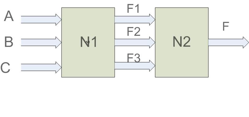
25 Multistage Logic Circuit Multistage Logic Circuit: N1 and N2 ; Two logic circuits. W, X, Y, Z: independent logic variables For each of the 16 possible combination of values for W, X, Y and Z, some specific value of A, B and C would be the outputs. Three variables normally have 8 possible sets of values.however, in the above circuit N1 may constrain the values to a smaller set. The remaining set of values for A, B and C would not affect the output of N2.Thus for N2, the non available inputs are called don t care inputs, since these inputs do not have any effect on F. 25
26 Don t care condition Example 1: x y w N1 A B N2 F z C Let A,B and C never have 001 or 110 values. Then for F, values of 001 and 110 for A, B and C are not of any importance. Exam 2: All possible input combinations are present. But the output is used in such a way that we do not care whether it is 0 or 1 for certain input combinations. F= m(0,3,7)+ d(1,6) Or F = Π M(2,4,5) Π D(1,6) 26
27 SIMPLIFICATION using KARNAUGH MAP Example: Given the Characteristic Table for a 2-stage network. (Please see the Figure in the next slide.) Solution: F1 = m (1,2,5,6) F2 = m(0,2,4,6) F3 = m (1,3,5,7) F= m (1, 2, 6 ), d(0, 3, 4, 7) Solution is continued in the next 3 slides. 27
28 28
29 SIMPLIFICATION using KARNAUGH MAP Designing for N1 F1 = m (1,2,5,6) F2 = m(0,2,4,6) F3 = m (1,3,5,7) F2=C F3=C F1=B C+BC 29
30 K- Map for F: Designing for N2 30
31 B N1 N2 31
This form sometimes used in logic circuit, example:
 Objectives: 1. Deriving of logical expression form truth tables. 2. Logical expression simplification methods: a. Algebraic manipulation. b. Karnaugh map (k-map). 1. Deriving of logical expression from
Karnaugh Maps Objectives
 Karnaugh Maps Objectives For Karnaugh Maps of up to 5 variables Plot a function from algebraic, minterm or maxterm form Obtain minimum Sum of Products and Product of Sums Understand the relationship between
Lecture 6: Manipulation of Algebraic Functions, Boolean Algebra, Karnaugh Maps
 EE210: Switching Systems Lecture 6: Manipulation of Algebraic Functions, Boolean Algebra, Karnaugh Maps Prof. YingLi Tian Feb. 21/26, 2019 Department of Electrical Engineering The City College of New York
Unit 2 Session - 6 Combinational Logic Circuits
 Objectives Unit 2 Session - 6 Combinational Logic Circuits Draw 3- variable and 4- variable Karnaugh maps and use them to simplify Boolean expressions Understand don t Care Conditions Use the Product-of-Sums
Advanced Digital Design with the Verilog HDL, Second Edition Michael D. Ciletti Prentice Hall, Pearson Education, 2011
 Problem 2-1 Recall that a minterm is a cube in which every variable appears. A Boolean expression in SOP form is canonical if every cube in the expression has a unique representation in which all of the
CHAPTER III BOOLEAN ALGEBRA
 CHAPTER III- CHAPTER III CHAPTER III R.M. Dansereau; v.. CHAPTER III-2 BOOLEAN VALUES INTRODUCTION BOOLEAN VALUES Boolean algebra is a form of algebra that deals with single digit binary values and variables.
CHAPTER III BOOLEAN ALGEBRA
 CHAPTER III- CHAPTER III CHAPTER III R.M. Dansereau; v.. CHAPTER III-2 BOOLEAN VALUES INTRODUCTION BOOLEAN VALUES Boolean algebra is a form of algebra that deals with single digit binary values and variables.
CHAPTER 5 KARNAUGH MAPS
 CHAPTER 5 1/36 KARNAUGH MAPS This chapter in the book includes: Objectives Study Guide 5.1 Minimum Forms of Switching Functions 5.2 Two- and Three-Variable Karnaugh Maps 5.3 Four-Variable Karnaugh Maps
UNIT 5 KARNAUGH MAPS Spring 2011
 UNIT 5 KRNUGH MPS Spring 2 Karnaugh Maps 2 Contents Minimum forms of switching functions Two- and three-variable Four-variable Determination of minimum expressions using essential prime implicants Five-variable
Digital Logic Design. Combinational Logic
 Digital Logic Design Combinational Logic Minterms A product term is a term where literals are ANDed. Example: x y, xz, xyz, A minterm is a product term in which all variables appear exactly once, in normal
Lecture 7: Karnaugh Map, Don t Cares
 EE210: Switching Systems Lecture 7: Karnaugh Map, Don t Cares Prof. YingLi Tian Feb. 28, 2019 Department of Electrical Engineering The City College of New York The City University of New York (CUNY) 1
Midterm1 Review. Jan 24 Armita
 Midterm1 Review Jan 24 Armita Outline Boolean Algebra Axioms closure, Identity elements, complements, commutativity, distributivity theorems Associativity, Duality, De Morgan, Consensus theorem Shannon
211: Computer Architecture Summer 2016
 211: Computer Architecture Summer 2016 Liu Liu Topic: Storage Project3 Digital Logic - Storage: Recap - Review: cache hit rate - Project3 - Digital Logic: - truth table => SOP - simplification: Boolean
Karnaugh Map & Boolean Expression Simplification
 Karnaugh Map & Boolean Expression Simplification Mapping a Standard POS Expression For a Standard POS expression, a 0 is placed in the cell corresponding to the product term (maxterm) present in the expression.
CSE 140: Components and Design Techniques for Digital Systems
 Lecture 4: Four Input K-Maps CSE 4: Components and Design Techniques for Digital Systems CK Cheng Dept. of Computer Science and Engineering University of California, San Diego Outlines Boolean Algebra
Minimization techniques
 Pune Vidyarthi Griha s COLLEGE OF ENGINEERING, NSIK - 4 Minimization techniques By Prof. nand N. Gharu ssistant Professor Computer Department Combinational Logic Circuits Introduction Standard representation
Lecture 5: NAND, NOR and XOR Gates, Simplification of Algebraic Expressions
 EE210: Switching Systems Lecture 5: NAND, NOR and XOR Gates, Simplification of Algebraic Expressions Prof. YingLi Tian Feb. 15, 2018 Department of Electrical Engineering The City College of New York The
CPE100: Digital Logic Design I
 Chapter 2 Professor Brendan Morris, SEB 3216, brendan.morris@unlv.edu http://www.ee.unlv.edu/~b1morris/cpe100/ CPE100: Digital Logic Design I Section 1004: Dr. Morris Combinational Logic Design Chapter
UNIT 4 MINTERM AND MAXTERM EXPANSIONS
 UNIT 4 MINTERM AND MAXTERM EXPANSIONS Spring 2 Minterm and Maxterm Expansions 2 Contents Conversion of English sentences to Boolean equations Combinational logic design using a truth table Minterm and
The Karnaugh Map COE 202. Digital Logic Design. Dr. Muhamed Mudawar King Fahd University of Petroleum and Minerals
 The Karnaugh Map COE 202 Digital Logic Design Dr. Muhamed Mudawar King Fahd University of Petroleum and Minerals Presentation Outline Boolean Function Minimization The Karnaugh Map (K-Map) Two, Three,
Lecture 4: Four Input K-Maps
 Lecture 4: Four Input K-Maps CSE 4: Components and Design Techniques for Digital Systems Fall 24 CK Cheng Dept. of Computer Science and Engineering University of California, San Diego Outlines Boolean
Optimizations and Tradeoffs. Combinational Logic Optimization
 Optimizations and Tradeoffs Combinational Logic Optimization Optimization & Tradeoffs Up to this point, we haven t really considered how to optimize our designs. Optimization is the process of transforming
ELC224C. Karnaugh Maps
 KARNAUGH MAPS Function Simplification Algebraic Simplification Half Adder Introduction to K-maps How to use K-maps Converting to Minterms Form Prime Implicants and Essential Prime Implicants Example on
ELCT201: DIGITAL LOGIC DESIGN
 ELCT2: DIGITAL LOGIC DESIGN Dr. Eng. Haitham Omran, haitham.omran@guc.edu.eg Dr. Eng. Wassim Alexan, wassim.joseph@guc.edu.eg Lecture 2 Following the slides of Dr. Ahmed H. Madian ذو الحجة 438 ه Winter
Lecture 6: Gate Level Minimization Syed M. Mahmud, Ph.D ECE Department Wayne State University
 Lecture 6: Gate Level Minimization Syed M. Mahmud, Ph.D ECE Department Wayne State University Original Source: Aby K George, ECE Department, Wayne State University Contents The Map method Two variable
Karnaugh Maps (K-Maps)
") Karnaugh Maps (K-Maps) Boolean expressions can be minimized by combining terms P + P = P K-maps minimize equations graphically Put terms to combine close to one another B C C B B C BC BC BC BC BC BC BC
Karnaugh Maps (K-Maps) Boolean expressions can be minimized by combining terms P + P = P K-maps minimize equations graphically Put terms to combine close to one another B C C B B C BC BC BC BC BC BC BC
Logical Design of Digital Systems
 Lecture 4 Table of Content 1. Combinational circuit design 2. Elementary combinatorial circuits for data transmission 3. Memory structures 4. Programmable logic devices 5. Algorithmic minimization approaches
Chapter 2 Combinational Logic Circuits
 Logic and Computer Design Fundamentals Chapter 2 Combinational Logic Circuits Part 2 Circuit Optimization Goal: To obtain the simplest implementation for a given function Optimization is a more formal
Combinational Logic Circuits Part II -Theoretical Foundations
 Combinational Logic Circuits Part II -Theoretical Foundations Overview Boolean Algebra Basic Logic Operations Basic Identities Basic Principles, Properties, and Theorems Boolean Function and Representations
Computer Organization I. Lecture 13: Design of Combinational Logic Circuits
 Computer Organization I Lecture 13: Design of Combinational Logic Circuits Overview The optimization of multiple-level circuits Mapping Technology Verification Objectives To know how to optimize the multiple-level
Working with Combinational Logic. Design example: 2x2-bit multiplier
 Working with ombinational Logic Simplification two-level simplification exploiting don t cares algorithm for simplification Logic realization two-level logic and canonical forms realized with NNs and NORs
Administrative Notes. Chapter 2 <9>
 Administrative Notes Note: New homework instructions starting with HW03 Homework is due at the beginning of class Homework must be organized, legible (messy is not), and stapled to be graded Chapter 2
Simplifying Logic Circuits with Karnaugh Maps
 Simplifying Logic Circuits with Karnaugh Maps The circuit at the top right is the logic equivalent of the Boolean expression: f = abc + abc + abc Now, as we have seen, this expression can be simplified
Gate-Level Minimization
 Gate-Level Minimization Dr. Bassem A. Abdullah Computer and Systems Department Lectures Prepared by Dr.Mona Safar, Edited and Lectured by Dr.Bassem A. Abdullah Outline 1. The Map Method 2. Four-variable
CSE 140 Midterm I - Solution
 CSE 140 Midterm I - Solution 1. Answer the following questions given the logic circuit below. (15 points) a. (5 points) How many CMOS transistors does the given (unsimplified) circuit have. b. (6 points)
Chapter 4 Optimized Implementation of Logic Functions
 Chapter 4 Optimized Implementation of Logic Functions Logic Minimization Karnaugh Maps Systematic Approach for Logic Minimization Minimization of Incompletely Specified Functions Tabular Method for Minimization
Ex: Boolean expression for majority function F = A'BC + AB'C + ABC ' + ABC.
 Boolean Expression Forms: Sum-of-products (SOP) Write an AND term for each input combination that produces a 1 output. Write the input variable if its value is 1; write its complement otherwise. OR the
Principles of Computer Architecture. Appendix B: Reduction of Digital Logic. Chapter Contents
 B-1 Principles of Computer Architecture Miles Murdocca and Vincent Heuring Appendix B: Reduction of Digital Logic B-2 Chapter Contents B.1 Reduction of Combinational Logic and Sequential Logic B.2 Reduction
Combinational Logic. Review of Combinational Logic 1
 Combinational Logic! Switches -> Boolean algebra! Representation of Boolean functions! Logic circuit elements - logic gates! Regular logic structures! Timing behavior of combinational logic! HDLs and combinational
Digital Circuit And Logic Design I. Lecture 4
 Digital Circuit And Logic Design I Lecture 4 Outline Combinational Logic Design Principles (2) 1. Combinational-circuit minimization 2. Karnaugh maps 3. Quine-McCluskey procedure Panupong Sornkhom, 2005/2
Total Time = 90 Minutes, Total Marks = 50. Total /50 /10 /18
 University of Waterloo Department of Electrical & Computer Engineering E&CE 223 Digital Circuits and Systems Midterm Examination Instructor: M. Sachdev October 23rd, 2007 Total Time = 90 Minutes, Total
Combinational Logic Fundamentals
 Topic 3: Combinational Logic Fundamentals In this note we will study combinational logic, which is the part of digital logic that uses Boolean algebra. All the concepts presented in combinational logic
EECS150 - Digital Design Lecture 19 - Combinational Logic Circuits : A Deep Dive
 EECS150 - Digital Design Lecture 19 - Combinational Logic Circuits : A Deep Dive March 30, 2010 John Wawrzynek Spring 2010 EECS150 - Lec19-cl1 Page 1 Boolean Algebra I (Representations of Combinational
Chapter 2. Digital Logic Basics
 Chapter 2 Digital Logic Basics 1 2 Chapter 2 2 1 Implementation using NND gates: We can write the XOR logical expression B + B using double negation as B+ B = B+B = B B From this logical expression, we
L4: Karnaugh diagrams, two-, and multi-level minimization. Elena Dubrova KTH / ICT / ES
 L4: Karnaugh diagrams, two-, and multi-level minimization Elena Dubrova KTH / ICT / ES dubrova@kth.se Combinatorial system a(t) not(a(t)) A combinatorial system has no memory - its output depends therefore
MC9211 Computer Organization
 MC92 Computer Organization Unit : Digital Fundamentals Lesson2 : Boolean Algebra and Simplification (KSB) (MCA) (29-2/ODD) (29 - / A&B) Coverage Lesson2 Introduces the basic postulates of Boolean Algebra
II. COMBINATIONAL LOGIC DESIGN. - algebra defined on a set of 2 elements, {0, 1}, with binary operators multiply (AND), add (OR), and invert (NOT):
, add (OR), and invert (NOT):") ENGI 386 Digital Logic II. COMBINATIONAL LOGIC DESIGN Combinational Logic output of digital system is only dependent on current inputs (i.e., no memory) (a) Boolean Algebra - developed by George Boole
ENGI 386 Digital Logic II. COMBINATIONAL LOGIC DESIGN Combinational Logic output of digital system is only dependent on current inputs (i.e., no memory) (a) Boolean Algebra - developed by George Boole
Chapter 7 Logic Circuits
 Chapter 7 Logic Circuits Goal. Advantages of digital technology compared to analog technology. 2. Terminology of Digital Circuits. 3. Convert Numbers between Decimal, Binary and Other forms. 5. Binary
Slide Set 3. for ENEL 353 Fall Steve Norman, PhD, PEng. Electrical & Computer Engineering Schulich School of Engineering University of Calgary
 Slide Set 3 for ENEL 353 Fall 2016 Steve Norman, PhD, PEng Electrical & Computer Engineering Schulich School of Engineering University of Calgary Fall Term, 2016 SN s ENEL 353 Fall 2016 Slide Set 3 slide
BOOLEAN ALGEBRA CLASS XII. Presented By : Dinesh Patel PGT CS KV IIT Powai
 BOOLEAN ALGEBRA CLASS II Presented By : Dinesh Patel PGT CS KV IIT Powai Introduction Boolean Algebra is a set of rules and regulation which is suitable for Digital Circuits, whose answer is either True
COM111 Introduction to Computer Engineering (Fall ) NOTES 6 -- page 1 of 12
 NOTES 6 -- page 1 of 12") COM111 Introduction to Computer Engineering (Fall 2006-2007) NOTES 6 -- page 1 of 12 Karnaugh Maps In this lecture, we will discuss Karnaugh maps (K-maps) more formally than last time and discuss a more
COM111 Introduction to Computer Engineering (Fall 2006-2007) NOTES 6 -- page 1 of 12 Karnaugh Maps In this lecture, we will discuss Karnaugh maps (K-maps) more formally than last time and discuss a more
EE40 Lec 15. Logic Synthesis and Sequential Logic Circuits
 EE40 Lec 15 Logic Synthesis and Sequential Logic Circuits Prof. Nathan Cheung 10/20/2009 Reading: Hambley Chapters 7.4-7.6 Karnaugh Maps: Read following before reading textbook http://www.facstaff.bucknell.edu/mastascu/elessonshtml/logic/logic3.html
EEE130 Digital Electronics I Lecture #4
 EEE130 Digital Electronics I Lecture #4 - Boolean Algebra and Logic Simplification - By Dr. Shahrel A. Suandi Topics to be discussed 4-1 Boolean Operations and Expressions 4-2 Laws and Rules of Boolean
Slides for Lecture 10
 Slides for Lecture 10 ENEL 353: Digital Circuits Fall 2013 Term Steve Norman, PhD, PEng Electrical & Computer Engineering Schulich School of Engineering University of Calgary 30 September, 2013 ENEL 353
Number System conversions
 Number System conversions Number Systems The system used to count discrete units is called number system. There are four systems of arithmetic which are often used in digital electronics. Decimal Number
Karnaugh Maps ف ر آ ا د : ا ا ب ا م آ ه ا ن ر ا
 Karnaugh Maps مخطط آارنوف اعداد:محمد اسماعيل آلية علوم الحاسوب جامعة امدرمان الاهلية الاهداء الي آل من يسلك طريق العلم والمعرفة في هذا المجال Venn Diagrams Venn diagram to represent the space of minterms.
14:332:231 DIGITAL LOGIC DESIGN
 :: DIGITAL LOGIC DESIGN Ivan Marsic, Rutgers University Electrical & Computer Engineering Fall Lecture #: Combinational Circuit Synthesis II hat if we have input variables? V = V = of Example with variables
CprE 281: Digital Logic
 CprE 28: Digital Logic Instructor: Alexander Stoytchev http://www.ece.iastate.edu/~alexs/classes/ Examples of Solved Problems CprE 28: Digital Logic Iowa State University, Ames, IA Copyright Alexander
Standard Expression Forms
 ThisLecture will cover the following points: Canonical and Standard Forms MinTerms and MaxTerms Digital Logic Families 24 March 2010 Standard Expression Forms Two standard (canonical) expression forms
ENG2410 Digital Design Combinational Logic Circuits
 ENG240 Digital Design Combinational Logic Circuits Fall 207 S. Areibi School of Engineering University of Guelph Binary variables Binary Logic Can be 0 or (T or F, low or high) Variables named with single
WEEK 3.1 MORE ON KARNAUGH MAPS
 WEEK 3. MORE ON KARNAUGH MAPS Don t Cares Sometimes, we might have inputs and it doesn t matter what the output is; i.e., we don t care what the output is. These situations are called don t cares. Rather
14:332:231 DIGITAL LOGIC DESIGN. Combinational Circuit Synthesis
 :: DIGITAL LOGIC DESIGN Ivan Marsic, Rutgers University Electrical & Computer Engineering all Lecture #: Combinational Circuit Synthesis I Combinational Circuit Synthesis Recall: Combinational circuit
Review. EECS Components and Design Techniques for Digital Systems. Lec 06 Minimizing Boolean Logic 9/ Review: Canonical Forms
 Review EECS 150 - Components and Design Techniques for Digital Systems Lec 06 Minimizing Boolean Logic 9/16-04 David Culler Electrical Engineering and Computer Sciences University of California, Berkeley
Chapter 2 Combinational Logic Circuits
 Logic and Computer Design Fundamentals Chapter 2 Combinational Logic Circuits Part 2 Circuit Optimization Charles Kime & Thomas Kaminski 2004 Pearson Education, Inc. Terms of Use (Hyperlinks are active
Combinational Logic Design/Circuits
 3 ` Combinational Logic Design/Circuits Chapter-3(Hours : 12 Marks:24 ) Combinational Logic design / Circuits 3.1 Simplification of Boolean expression using Boolean algebra. 3.2 Construction of logical
E&CE 223 Digital Circuits & Systems. Lecture Transparencies (Boolean Algebra & Logic Gates) M. Sachdev
 M. Sachdev") E&CE 223 Digital Circuits & Systems Lecture Transparencies (Boolean Algebra & Logic Gates) M. Sachdev 4 of 92 Section 2: Boolean Algebra & Logic Gates Major topics Boolean algebra NAND & NOR gates Boolean
E&CE 223 Digital Circuits & Systems Lecture Transparencies (Boolean Algebra & Logic Gates) M. Sachdev 4 of 92 Section 2: Boolean Algebra & Logic Gates Major topics Boolean algebra NAND & NOR gates Boolean
Chap 2. Combinational Logic Circuits
 Overview 2 Chap 2. Combinational Logic Circuits Spring 24 Part Gate Circuits and Boolean Equations Binary Logic and Gates Boolean Algebra Standard Forms Part 2 Circuit Optimization Two-Level Optimization
DIGITAL ELECTRONICS & it0203 Semester 3
 DIGITAL ELECTRONICS & it0203 Semester 3 P.Rajasekar & C.M.T.Karthigeyan Asst.Professor SRM University, Kattankulathur School of Computing, Department of IT 8/22/2011 1 Disclaimer The contents of the slides
E&CE 223 Digital Circuits & Systems. Lecture Transparencies (Boolean Algebra & Logic Gates) M. Sachdev. Section 2: Boolean Algebra & Logic Gates
 M. Sachdev. Section 2: Boolean Algebra & Logic Gates") Digital Circuits & Systems Lecture Transparencies (Boolean lgebra & Logic Gates) M. Sachdev 4 of 92 Section 2: Boolean lgebra & Logic Gates Major topics Boolean algebra NND & NOR gates Boolean algebra
Digital Circuits & Systems Lecture Transparencies (Boolean lgebra & Logic Gates) M. Sachdev 4 of 92 Section 2: Boolean lgebra & Logic Gates Major topics Boolean algebra NND & NOR gates Boolean algebra
Review for Test 1 : Ch1 5
 Review for Test 1 : Ch1 5 October 5, 2006 Typeset by FoilTEX Positional Numbers 527.46 10 = (5 10 2 )+(2 10 1 )+(7 10 0 )+(4 10 1 )+(6 10 2 ) 527.46 8 = (5 8 2 ) + (2 8 1 ) + (7 8 0 ) + (4 8 1 ) + (6 8
Boolean Algebra and Logic Design (Class 2.2 1/24/2013) CSE 2441 Introduction to Digital Logic Spring 2013 Instructor Bill Carroll, Professor of CSE
 CSE 2441 Introduction to Digital Logic Spring 2013 Instructor Bill Carroll, Professor of CSE") Boolean Algebra and Logic Design (Class 2.2 1/24/2013) CSE 2441 Introduction to Digital Logic Spring 2013 Instructor Bill Carroll, Professor of CSE Today s Topics Boolean algebra applications in logic
Boolean Algebra and Logic Design (Class 2.2 1/24/2013) CSE 2441 Introduction to Digital Logic Spring 2013 Instructor Bill Carroll, Professor of CSE Today s Topics Boolean algebra applications in logic
Logic Design Combinational Circuits. Digital Computer Design
 Logic Design Combinational Circuits Digital Computer Design Topics Combinational Logic Karnaugh Maps Combinational uilding locks Timing 2 Logic Circuit logic circuit is composed of: Inputs Outputs Functional
Chapter 2 Combinational Logic Circuits
 Logic and Computer Design Fundamentals Chapter 2 Combinational Logic Circuits Part 1 Gate Circuits and Boolean Equations Charles Kime & Thomas Kaminski 2008 Pearson Education, Inc. (Hyperlinks are active
Chapter-2 BOOLEAN ALGEBRA
 Chapter-2 BOOLEAN ALGEBRA Introduction: An algebra that deals with binary number system is called Boolean Algebra. It is very power in designing logic circuits used by the processor of computer system.
Chapter 4 BOOLEAN ALGEBRA AND THEOREMS, MINI TERMS AND MAX TERMS
 Chapter 4 BOOLEAN ALGEBRA AND THEOREMS, MINI TERMS AND MAX TERMS Lesson 4 BOOLEAN EXPRESSION, TRUTH TABLE and SUM OF THE PRODUCTS (SOPs) [MINITERMS] 2 Outline SOP two variables cases SOP for three variable
for Digital Systems Simplification of logic functions Tajana Simunic Rosing Sources: TSR, Katz, Boriello & Vahid
 SE140: omponents and Design Techniques for Digital Systems Simplification of logic functions Tajana Simunic Rosing 1 What we covered thus far: Number representations Where we are now inary, Octal, Hex,
Outcomes. Spiral 1 / Unit 5. Logic Function Synthesis KARNAUGH MAPS. Karnaugh Maps
 -. -. Spiral / Unit Mark Redekopp Outcomes I know the difference between combinational and sequential logic and can name examples of each. I understand latency, throughput, and at least technique to improve
Spiral 1 / Unit 5. Karnaugh Maps
 -. Spiral / Unit Karnaugh Maps -. Outcomes I know the difference between combinational and sequential logic and can name examples of each. I understand latency, throughput, and at least technique to improve
ENGG 1203 Tutorial - 2 Recall Lab 2 - e.g. 4 input XOR. Parity checking (for interest) Recall : Simplification methods. Recall : Time Delay
 Recall : Simplification methods. Recall : Time Delay") ENGG 23 Tutorial - 2 Recall Lab 2 - e.g. 4 input XOR Parity checking (for interest) Parity bit Parity checking Error detection, eg. Data can be Corrupted Even parity total number of s is even Odd parity
ENGG 23 Tutorial - 2 Recall Lab 2 - e.g. 4 input XOR Parity checking (for interest) Parity bit Parity checking Error detection, eg. Data can be Corrupted Even parity total number of s is even Odd parity
Binary logic consists of binary variables and logical operations. The variables are
 1) Define binary logic? Binary logic consists of binary variables and logical operations. The variables are designated by the alphabets such as A, B, C, x, y, z, etc., with each variable having only two
Chapter 2 Boolean Algebra and Logic Gates
 Ch1: Digital Systems and Binary Numbers Ch2: Ch3: Gate-Level Minimization Ch4: Combinational Logic Ch5: Synchronous Sequential Logic Ch6: Registers and Counters Switching Theory & Logic Design Prof. Adnan
Functions. Computers take inputs and produce outputs, just like functions in math! Mathematical functions can be expressed in two ways:
 Boolean Algebra (1) Functions Computers take inputs and produce outputs, just like functions in math! Mathematical functions can be expressed in two ways: An expression is finite but not unique f(x,y)
Boolean Algebra and Logic Simplification
 S302 Digital Logic Design Boolean Algebra and Logic Simplification Boolean Analysis of Logic ircuits, evaluating of Boolean expressions, representing the operation of Logic circuits and Boolean expressions
Outcomes. Spiral 1 / Unit 5. Logic Function Synthesis KARNAUGH MAPS. Karnaugh Maps
 -. -. Spiral / Unit Mark Redekopp Outcomes I know the difference between combinational and sequential logic and can name examples of each. I understand latency, throughput, and at least technique to improve
ECEN 248: INTRODUCTION TO DIGITAL SYSTEMS DESIGN. Week 2 Dr. Srinivas Shakkottai Dept. of Electrical and Computer Engineering
 ECEN 248: INTRODUCTION TO DIGITAL SYSTEMS DESIGN Week 2 Dr. Srinivas Shakkottai Dept. of Electrical and Computer Engineering Boolean Algebra Boolean Algebra A Boolean algebra is defined with: A set of
Ch 2. Combinational Logic. II - Combinational Logic Contemporary Logic Design 1
 Ch 2. Combinational Logic II - Combinational Logic Contemporary Logic Design 1 Combinational logic Define The kind of digital system whose output behavior depends only on the current inputs memoryless:
Chapter 2 : Boolean Algebra and Logic Gates
 Chapter 2 : Boolean Algebra and Logic Gates By Electrical Engineering Department College of Engineering King Saud University 1431-1432 2.1. Basic Definitions 2.2. Basic Theorems and Properties of Boolean
CS 121 Digital Logic Design. Chapter 2. Teacher Assistant. Hanin Abdulrahman
 CS 121 Digital Logic Design Chapter 2 Teacher Assistant Hanin Abdulrahman 1 2 Outline 2.2 Basic Definitions 2.3 Axiomatic Definition of Boolean Algebra. 2.4 Basic Theorems and Properties 2.5 Boolean Functions
Week-I. Combinational Logic & Circuits
 Week-I Combinational Logic & Circuits Overview Binary logic operations and gates Switching algebra Algebraic Minimization Standard forms Karnaugh Map Minimization Other logic operators IC families and
Part 1: Digital Logic and Gates. Analog vs. Digital waveforms. The digital advantage. In real life...
 Part 1: Digital Logic and Gates Analog vs Digital waveforms An analog signal assumes a continuous range of values: v(t) ANALOG A digital signal assumes discrete (isolated, separate) values Usually there
Computer Organization I
 Computer Organization I Lecture 6: Boolean Algebra /2/29 Wei Lu CS283 Overview Two Principles in Boolean Algebra () Duality Principle (2) Complement Principle Standard Form of Logic Expression () Sum of
EXPERIMENT #4: SIMPLIFICATION OF BOOLEAN FUNCTIONS
 EXPERIMENT #4: SIMPLIFICATION OF BOOLEAN FUNCTIONS OBJECTIVES: Simplify Boolean functions using K-map method Obtain Boolean expressions from timing diagrams Design and implement logic circuits Equipment
Chapter 2 Combinational Logic Circuits
 Logic and Computer Design Fundamentals Chapter 2 Combinational Logic Circuits Part 1 Gate Circuits and Boolean Equations Charles Kime & Thomas Kaminski 2008 Pearson Education, Inc. Overview Part 1 Gate
CS 226: Digital Logic Design
 CS 226: Digital Logic Design 0 1 1 I S 0 1 0 S Department of Computer Science and Engineering, Indian Institute of Technology Bombay. 1 of 29 Objectives In this lecture we will introduce: 1. Logic functions
ENGR 303 Introduction to Logic Design Lecture 3. Dr. Chuck Brown Engineering and Computer Information Science Folsom Lake College
 Introduction to Logic Design Lecture 3 Dr. Chuck rown Engineering and Computer Information Science Folsom Lake College Outline for Todays Lecture Logic Circuits SOP / POS oolean Theorems DeMorgan s Theorem
Combinatorial Logic Design Principles
 Combinatorial Logic Design Principles ECGR2181 Chapter 4 Notes Logic System Design I 4-1 Boolean algebra a.k.a. switching algebra deals with boolean values -- 0, 1 Positive-logic convention analog voltages
Logic Simplification. Boolean Simplification Example. Applying Boolean Identities F = A B C + A B C + A BC + ABC. Karnaugh Maps 2/10/2009 COMP370 1
 Digital Logic COMP370 Introduction to Computer Architecture Logic Simplification It is frequently possible to simplify a logical expression. This makes it easier to understand and requires fewer gates
Lecture 2 Review on Digital Logic (Part 1)
") Lecture 2 Review on Digital Logic (Part 1) Xuan Silvia Zhang Washington University in St. Louis http://classes.engineering.wustl.edu/ese461/ Grading Engagement 5% Review Quiz 10% Homework 10% Labs 40%
Lecture 2 Review on Digital Logic (Part 1) Xuan Silvia Zhang Washington University in St. Louis http://classes.engineering.wustl.edu/ese461/ Grading Engagement 5% Review Quiz 10% Homework 10% Labs 40%
Chapter 2 Combinational Logic Circuits
 Logic and Computer Design Fundamentals Chapter 2 Combinational Logic Circuits Part 1 Gate Circuits and Boolean Equations Chapter 2 - Part 1 2 Chapter 2 - Part 1 3 Chapter 2 - Part 1 4 Chapter 2 - Part
Logic Gate Level. Part 2
 Logic Gate Level Part 2 Constructing Boolean expression from First method: write nonparenthesized OR of ANDs Each AND is a 1 in the result column of the truth table Works best for table with relatively