Memories Bipolar Transistors
|
|
|
- Harry Crawford
- 5 years ago
- Views:
Transcription
1 Technische Universität Graz nstitute of Solid State Physics Memories Bipolar Transistors
2 Technische Universität Graz nstitute of Solid State Physics Exams February 5 March 7 April 18 June 27
3 Exam Four questions, two from the online list. Calculator is ok. No notes. Explain some concept: (tunnel contact, indirect band gap, thermionic emission, inversion, threshold voltage,...) Perform a calculation: (concentration of minority carriers, integrate charge density to find electric field,...) Explain how a device works: (JFET, MESFET, MOSFET, laser diode, bipolar transistor, LED, Schottky diode, Heterojunction bipolar transistor,...)
4 Gate delay Gate delay is limited by C gate V dd /. Ring oscillator
5 SRAM Static random access memory No refresh circuitry needed.

6 DRAM Dynamic random access memory
7 DRAM Read and refresh DRAM with a SRAM cell

8 Flash memory Charge is stored on a floating gate nonvolatile

9 Phase change memory Phase-change memory (PRAM) uses chalcogenide materials. These can be switched between a low resistance crystalline state and a high resistance amorphous state. GeSbTe is melted by a laser in rewritable DVDs and by a current in PRAM. nonvolatile


10 High Bandwidth Memory AMD to launch its HBM graphics cards on 16 June 2015.
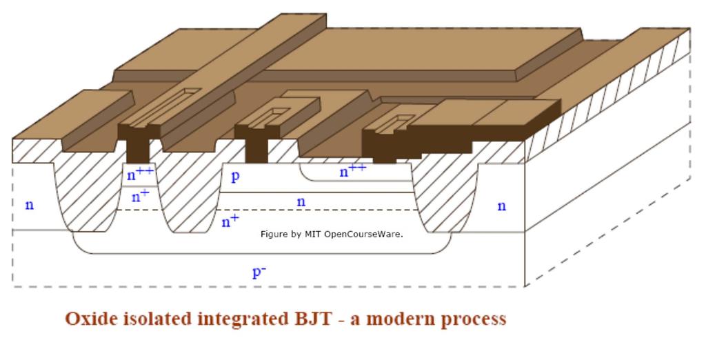
11 Technische Universität Graz nstitute of Solid State Physics bipolar transistors npn transistor collector base emitter n+ n p+ p n + lightly doped p substrate Used in front-end high-frequency receivers (mobile telephones).
12 bipolar transistors p+
13 abrupt junction de dx E dv dx E en A + -x p - x n en D x A E xxp -x p x n x ev bi D A kbt ln 2 ni en en D E xxn 2 en A x V xxp xp x0 2 2 en D x V xxn 0 x x 2 N N x x0 p 0 x x n n
 NDexp kt B ev np0 exp kt B evbi V pn( xn) NAexp kt B ev pn0 exp kt B Minority electrons are injected into the p-region")
14 Forward bias, V > 0 n p0 N A n N 2 i A ND p n0 n p (x p ) p n (x n ) + n N 2 i D Electrons and holes are driven towards the junction. The depletion region becomes narrower evbi V np( xp) NDexp kt B ev np0 exp kt B evbi V pn( xn) NAexp kt B ev pn0 exp kt B Minority electrons are injected into the p-region Minority holes are injected into the n-region
 NDexp kt B ev np0 exp kt B ev bi V pn( xn) NAexp kt B ev pn0 exp kt B Minority electrons are extracted from the p-region by the electric field")
15 Reverse bias, V < 0 n p0 N A n N 2 i A n p (x p ) p n (x n ) + p ND n0 n N 2 i D Electrons and holes are driven away from the junction. The depletion region becomes wider evbi V np( xp) NDexp kt B ev np0 exp kt B ev bi V pn( xn) NAexp kt B ev pn0 exp kt B Minority electrons are extracted from the p-region by the electric field Minority holes are extracted from the n-region by the electric field
16 pnp transistor, no bias
17 pnp transistor, forward active bias The base-emitter voltage controls the minority carriers injected from the emitter to the base. These diffuse to the base-collector junction and are swept into the collector. Always dissipate power due to the forward bias
18 Long/Short diode p n (x n ) Long diode d n >> L p p n (x n ) p n0 p n (x) d n n-type dp J ed ed dx diff, p p p x Short diode d n << L p Metal contact is much closer to the depletion region than the diffusion length J diff, p p ( x ) p n n n0 d n dp edp dx
19 Minority carrier concentration contact p emitter (n+) base (p) collector (n) exp ev be nb0 ev kt B kt B e0 exp be contact n b0 p c0 p exp ev bc nb0 e0 kt B x e We W eb W bc W x c c evbe / kbt pe0 e 1 exp ev bc pc0 kt B Ep eabedp W x ea D En be n b0 n e e e e ev / k T ev / k T be B bc B W bc W be
20 Emitter current ea D p ea D n e ea D n e be B bc B 1 1 be p e 0 be n b0 ev / k T be n b0 ev / k T E En Ep Web xe Wbc Wbe Wbc Wbe evbe / kbt / 1 evbc kbt 1 e e E ES R CS p ev kt B e0 exp be n ev kt B b0 exp be p e0 n b0 exp ev bc nb0 kt B x e We W eb W x bc W c c p c0
21 Collector current contact p emitter (n+) base (p) collector (n) exp ev be nb0 ev kt B kt B e0 exp be contact n b0 p c0 p exp ev bc nb0 e0 kt B x e We W eb W bc W x c c evbc / kbt pc0 e 1 exp ev bc pc0 kt B cp eabcdp x W ea D cn bc n b0 n e e c ev / k T ev / k T c be B bc B W bc W eb
22 Collector current ea D n ea D p ea D n evbe / kbt bc p c0 evbc 1 / kbt 1 bc n b0 bc n b0 c cp cn e e Wbc Wbe xc Wc Wbc Wbe evbe / kt B / 1 evbc kt B 1 e e c cp cn F ES CS p ev kt B e0 exp be n ev kt B b0 exp be p e0 n b0 exp ev bc nb0 kt B x e We W eb W x bc W c c p c0

 exp ev be")


23 Not an npn transistor contact p e0 exp be emitter (n+) base (p) collector (n) exp ev be nb0 ev kt B kt B contact n b0 p c0 p exp ev bc nb0 e0 kt B x e We W eb W x bc W c c exp ev bc pc0 kt B
24 Ebers-Moll model evbe / kbt / 1 evbc kbt 1 e e E ES R CS evbe / kbt / 1 evbc kbt 1 e e C F ES CS B E C B E R F F R C F evbe / kbt evbc / kbt ES 1 R CS e 1 e
25 Emitter efficiency e En 1 1 / En Ep Ep En for npn ea D Ep be p ea D En be n b0 p evbe / kbt e0 e 1 W eb x n e e e ev / k T ev / k T be B bc B W bc W be For e ~ 1, W bc -W be << L b, W eb -x e and n b0 >> p e0 neutral base width Small base width and heavy emitter doping n N 2 i Ab n N 2 i De
26 Base transport factor B c En ratio of the injected current to the collected current recombination in the base would reduce the base transport factor A thin base with low doping results in a base transport factor ~ 1
27 Current transfer ratio C E B e ~ 1 for a good BJT
28 Transistor modes 1. Forward active: emitter-base forward, base-collector reverse 2. Saturation: emitter-base forward, base-collector forward 3. Reverse active: emitter-base reverse, base-collector forward 4. Cut-off: emitter-base reverse, base-collector reverse

29 Common base configuration evbe / kbt / 1 evbc kbt 1 e e E ES R CS solve for V be e e evbe / kt B / 1 evbc kt B 1 c F ES CS saturation active cutoff E < 0
30 Common base configuration c C ~ E buffer circuit: the output current is constant over a wide range of output voltages
31 Ebers - Moll Model ea D p ea D n ES W x W W eabednnb 0 RCS W W be p e0 be n b0 eb e bc be bc be F CS ES ea D n W W bc n b0 bc be ea D p ea D n x W W W bc p c0 bc n b0 c c bc be
32 Common emitter configuration evbe / kbt / 1 evbc kbt 1 e e E ES R CS evbe / kbt / 1 evbc kbt 1 e e c F ES CS current amplification ~100 B E C
33 Current amplification factor C fe B h B E C 1 1 B C 1 1 C e B e B B ~ C E
34 The Art of Electronics Horowitz and Hill for common emitter configuration
35 Transconductance g m V C be evbe / kt B / 1 evbc kt B 1 e e c F ES CS The first term depends on V be g m e e e e kt kt kt be B F ES ev / k T C B B B B The transconductance can be very high.
36 Early effect Ebers - Moll: evbe / kbt / 1 evbc kbt 1 e e E ES R CS evbe / kt B / 1 evbc kt B 1 e e c F ES CS B E C ES ea D p ea D n W x W W be p e0 be n b0 eb e bc be CS ea D p ea D n x W W W bc p c0 bc n b0 c c bc be ES and CS are treated as constants but the depletion widths W bc, W be, W c, and W e depend on the voltages. p ev kt B e0 exp be n ev kt B b0 exp be p ev kt B c0 exp bc n b0 p c0 p exp evbc nb 0 e0 kt B x e W e W eb W x bc W c c
37 Early effect Common emitter configuration Base width modulation: smaller width increases the diffusion current and increases the gain. Punchthrough: The neutral base width goes to zero and all gain is lost. Lightly dope the collector -> voltage drops in collector. Makes circuit slower.
38 Common emitter configuration C ~ B amplifier
12. Memories / Bipolar transistors
 Technische Universität Graz Institute of Solid State Physics 12. Memories / Bipolar transistors Jan. 9, 2019 Technische Universität Graz Institute of Solid State Physics Exams January 31 March 8 May 17
Institute of Solid State Physics. Technische Universität Graz. Exam. Feb 2, 10:00-11:00 P2
 Technische Universität Graz nstitute of Solid State Physics Exam Feb 2, 10:00-11:00 P2 Exam Four questions, two from the online list. Calculator is ok. No notes. Explain some concept: (tunnel contact,
13. Bipolar transistors
 Technische Universität Graz Institute of Solid State Physics 13. Bipolar transistors Jan. 16, 2019 Technische Universität Graz Institute of Solid State Physics bipolar transistors npn transistor collector
Current mechanisms Exam January 27, 2012
 Current mechanisms Exam January 27, 2012 There are four mechanisms that typically cause currents to flow: thermionic emission, diffusion, drift, and tunneling. Explain briefly which kind of current mechanisms
8. Schottky contacts / JFETs
 Technische Universität Graz Institute of Solid State Physics 8. Schottky contacts / JFETs Nov. 21, 2018 Technische Universität Graz Institute of Solid State Physics metal - semiconductor contacts Photoelectric
Schottky diodes. JFETs - MESFETs - MODFETs
 Technische Universität Graz Institute of Solid State Physics Schottky diodes JFETs - MESFETs - MODFETs Quasi Fermi level When the charge carriers are not in equilibrium the Fermi energy can be different
Avalanche breakdown. Impact ionization causes an avalanche of current. Occurs at low doping
 Avalanche breakdown Impact ionization causes an avalanche of current Occurs at low doping Zener tunneling Electrons tunnel from valence band to conduction band Occurs at high doping Tunneling wave decays
Device Physics: The Bipolar Transistor
 Monolithic Amplifier Circuits: Device Physics: The Bipolar Transistor Chapter 4 Jón Tómas Guðmundsson tumi@hi.is 2. Week Fall 2010 1 Introduction In analog design the transistors are not simply switches
EE105 - Fall 2006 Microelectronic Devices and Circuits
 EE105 - Fall 2006 Microelectronic Devices and Circuits Prof. Jan M. Rabaey (jan@eecs) Lecture 21: Bipolar Junction Transistor Administrative Midterm Th 6:30-8pm in Sibley Auditorium Covering everything
Lecture 17 - The Bipolar Junction Transistor (I) Forward Active Regime. April 10, 2003
 Forward Active Regime. April 10, 2003") 6.012 - Microelectronic Devices and Circuits - Spring 2003 Lecture 17-1 Lecture 17 - The Bipolar Junction Transistor (I) Contents: Forward Active Regime April 10, 2003 1. BJT: structure and basic operation
6.012 - Microelectronic Devices and Circuits - Spring 2003 Lecture 17-1 Lecture 17 - The Bipolar Junction Transistor (I) Contents: Forward Active Regime April 10, 2003 1. BJT: structure and basic operation
ECE-305: Spring 2018 Final Exam Review
 C-305: Spring 2018 Final xam Review Pierret, Semiconductor Device Fundamentals (SDF) Chapters 10 and 11 (pp. 371-385, 389-403) Professor Peter Bermel lectrical and Computer ngineering Purdue University,
Final Examination EE 130 December 16, 1997 Time allotted: 180 minutes
 Final Examination EE 130 December 16, 1997 Time allotted: 180 minutes Problem 1: Semiconductor Fundamentals [30 points] A uniformly doped silicon sample of length 100µm and cross-sectional area 100µm 2
Electronic Circuits 1. Transistor Devices. Contents BJT and FET Characteristics Operations. Prof. C.K. Tse: Transistor devices
 Electronic Circuits 1 Transistor Devices Contents BJT and FET Characteristics Operations 1 What is a transistor? Three-terminal device whose voltage-current relationship is controlled by a third voltage
ELEC 3908, Physical Electronics, Lecture 17. Bipolar Transistor Injection Models
 LC 3908, Physical lectronics, Lecture 17 Bipolar Transistor njection Models Lecture Outline Last lecture looked at qualitative operation of the BJT, now want to develop a quantitative model to predict
Introduction to Power Semiconductor Devices
 ECE442 Power Semiconductor Devices and Integrated Circuits Introduction to Power Semiconductor Devices Zheng Yang (ERF 3017, email: yangzhen@uic.edu) Power Semiconductor Devices Applications System Ratings
Lecture 17 The Bipolar Junction Transistor (I) Forward Active Regime
 Forward Active Regime") Lecture 17 The Bipolar Junction Transistor (I) Forward Active Regime Outline The Bipolar Junction Transistor (BJT): structure and basic operation I V characteristics in forward active regime Reading Assignment:
Lecture 17 The Bipolar Junction Transistor (I) Forward Active Regime Outline The Bipolar Junction Transistor (BJT): structure and basic operation I V characteristics in forward active regime Reading Assignment:
Spring Semester 2012 Final Exam
 Spring Semester 2012 Final Exam Note: Show your work, underline results, and always show units. Official exam time: 2.0 hours; an extension of at least 1.0 hour will be granted to anyone. Materials parameters
Lecture 35 - Bipolar Junction Transistor (cont.) November 27, Current-voltage characteristics of ideal BJT (cont.)
 November 27, Current-voltage characteristics of ideal BJT (cont.)") 6.720J/3.43J - Integrated Microelectronic Devices - Fall 2002 Lecture 35-1 Lecture 35 - Bipolar Junction Transistor (cont.) November 27, 2002 Contents: 1. Current-voltage characteristics of ideal BJT (cont.)
6.720J/3.43J - Integrated Microelectronic Devices - Fall 2002 Lecture 35-1 Lecture 35 - Bipolar Junction Transistor (cont.) November 27, 2002 Contents: 1. Current-voltage characteristics of ideal BJT (cont.)
Semiconductor Physics fall 2012 problems
 Semiconductor Physics fall 2012 problems 1. An n-type sample of silicon has a uniform density N D = 10 16 atoms cm -3 of arsenic, and a p-type silicon sample has N A = 10 15 atoms cm -3 of boron. For each
Semiconductor Physics Problems 2015
 Semiconductor Physics Problems 2015 Page and figure numbers refer to Semiconductor Devices Physics and Technology, 3rd edition, by SM Sze and M-K Lee 1. The purest semiconductor crystals it is possible
Digital Integrated CircuitDesign
 Digital Integrated CircuitDesign Lecture 5a Bipolar Transistor Dep. Region Neutral Base n(0) b B C n b0 P C0 P e0 P C xn 0 xp 0 x n(w) b W B Adib Abrishamifar EE Department IUST Contents Bipolar Transistor
Physics of Semiconductors 8 th
 Physics of Semiconductors 8 th 2016.6.6 Shingo Katsumoto Department of Physics, Institute for Solid State Physics University of Tokyo Review of pn junction Estimation of builtin potential Depletion layer
Lecture 19 - p-n Junction (cont.) October 18, Ideal p-n junction out of equilibrium (cont.) 2. pn junction diode: parasitics, dynamics
 October 18, Ideal p-n junction out of equilibrium (cont.) 2. pn junction diode: parasitics, dynamics") 6.720J/3.43J - Integrated Microelectronic Devices - Fall 2002 Lecture 19-1 Lecture 19 - p-n Junction (cont.) October 18, 2002 Contents: 1. Ideal p-n junction out of equilibrium (cont.) 2. pn junction diode:
6.720J/3.43J - Integrated Microelectronic Devices - Fall 2002 Lecture 19-1 Lecture 19 - p-n Junction (cont.) October 18, 2002 Contents: 1. Ideal p-n junction out of equilibrium (cont.) 2. pn junction diode:
Forward-Active Terminal Currents
 Forward-Active Terminal Currents Collector current: (electron diffusion current density) x (emitter area) diff J n AE qd n n po A E V E V th ------------------------------ e W (why minus sign? is by def.
Recitation 17: BJT-Basic Operation in FAR
 Recitation 17: BJT-Basic Operation in FAR BJT stands for Bipolar Junction Transistor 1. Can be thought of as two p-n junctions back to back, you can have pnp or npn. In analogy to MOSFET small current
CLASS 3&4. BJT currents, parameters and circuit configurations
 CLASS 3&4 BJT currents, parameters and circuit configurations I E =I Ep +I En I C =I Cp +I Cn I B =I BB +I En -I Cn I BB =I Ep -I Cp I E = I B + I C I En = current produced by the electrons injected from
UNIVERSITY OF CALIFORNIA, BERKELEY College of Engineering Department of Electrical Engineering and Computer Sciences
 UNIVERSITY OF CALIFORNIA, BERKELEY College of Engineering Department of Electrical Engineering and Computer Sciences EE 105: Microelectronic Devices and Circuits Spring 2008 MIDTERM EXAMINATION #1 Time
ECE 305 Fall Final Exam (Exam 5) Wednesday, December 13, 2017
 Wednesday, December 13, 2017") NAME: PUID: ECE 305 Fall 017 Final Exam (Exam 5) Wednesday, December 13, 017 This is a closed book exam. You may use a calculator and the formula sheet at the end of this exam. Following the ECE policy,
NAME: PUID: ECE 305 Fall 017 Final Exam (Exam 5) Wednesday, December 13, 017 This is a closed book exam. You may use a calculator and the formula sheet at the end of this exam. Following the ECE policy,
Schottky Rectifiers Zheng Yang (ERF 3017,
 ECE442 Power Semiconductor Devices and Integrated Circuits Schottky Rectifiers Zheng Yang (ERF 3017, email: yangzhen@uic.edu) Power Schottky Rectifier Structure 2 Metal-Semiconductor Contact The work function
ECE-342 Test 2 Solutions, Nov 4, :00-8:00pm, Closed Book (one page of notes allowed)
") ECE-342 Test 2 Solutions, Nov 4, 2008 6:00-8:00pm, Closed Book (one page of notes allowed) Please use the following physical constants in your calculations: Boltzmann s Constant: Electron Charge: Free
ECE-342 Test 2 Solutions, Nov 4, 2008 6:00-8:00pm, Closed Book (one page of notes allowed) Please use the following physical constants in your calculations: Boltzmann s Constant: Electron Charge: Free
ELEC 3908, Physical Electronics, Lecture 18. The Early Effect, Breakdown and Self-Heating
 ELEC 3908, Physical Electronics, Lecture 18 The Early Effect, Breakdown and Self-Heating Lecture Outline Previous 2 lectures analyzed fundamental static (dc) carrier transport in the bipolar transistor
Student Number: CARLETON UNIVERSITY SELECTED FINAL EXAMINATION QUESTIONS
 Name: CARLETON UNIVERSITY SELECTE FINAL EXAMINATION QUESTIONS URATION: 6 HOURS epartment Name & Course Number: ELEC 3908 Course Instructors: S. P. McGarry Authorized Memoranda: Non-programmable calculators
Lecture 17. The Bipolar Junction Transistor (II) Regimes of Operation. Outline
 Regimes of Operation. Outline") Lecture 17 The Bipolar Junction Transistor (II) Regimes of Operation Outline Regimes of operation Large-signal equivalent circuit model Output characteristics Reading Assignment: Howe and Sodini; Chapter
Lecture 17 The Bipolar Junction Transistor (II) Regimes of Operation Outline Regimes of operation Large-signal equivalent circuit model Output characteristics Reading Assignment: Howe and Sodini; Chapter
Biasing the CE Amplifier
 Biasing the CE Amplifier Graphical approach: plot I C as a function of the DC base-emitter voltage (note: normally plot vs. base current, so we must return to Ebers-Moll): I C I S e V BE V th I S e V th
figure shows a pnp transistor biased to operate in the active mode
 Lecture 10b EE-215 Electronic Devices and Circuits Asst Prof Muhammad Anis Chaudhary BJT: Device Structure and Physical Operation The pnp Transistor figure shows a pnp transistor biased to operate in the
R. Ludwig and G. Bogdanov RF Circuit Design: Theory and Applications 2 nd edition. Figures for Chapter 6
 R. Ludwig and G. Bogdanov RF Circuit Design: Theory and Applications 2 nd edition Figures for Chapter 6 Free electron Conduction band Hole W g W C Forbidden Band or Bandgap W V Electron energy Hole Valence
Charge-Storage Elements: Base-Charging Capacitance C b
 Charge-Storage Elements: Base-Charging Capacitance C b * Minority electrons are stored in the base -- this charge q NB is a function of the base-emitter voltage * base is still neutral... majority carriers
junctions produce nonlinear current voltage characteristics which can be exploited
 Chapter 6 P-N DODES Junctions between n-and p-type semiconductors are extremely important foravariety of devices. Diodes based on p-n junctions produce nonlinear current voltage characteristics which can
Metal-oxide-semiconductor field effect transistors (2 lectures)
") Metal-ide-semiconductor field effect transistors ( lectures) MOS physics (brief in book) Current-voltage characteristics - pinch-off / channel length modulation - weak inversion - velocity saturation -
Metal-ide-semiconductor field effect transistors ( lectures) MOS physics (brief in book) Current-voltage characteristics - pinch-off / channel length modulation - weak inversion - velocity saturation -
Bipolar junction transistor operation and modeling
 6.01 - Electronic Devices and Circuits Lecture 8 - Bipolar Junction Transistor Basics - Outline Announcements Handout - Lecture Outline and Summary; Old eam 1's on Stellar First Hour Eam - Oct. 8, 7:30-9:30
Lecture 27: Introduction to Bipolar Transistors
 NCN www.nanohub.org ECE606: Solid State Devices Lecture 27: Introduction to ipolar Transistors Muhammad Ashraful Alam alam@purdue.edu Alam ECE 606 S09 1 ackground E C E C ase! Point contact Germanium transistor
For the following statements, mark ( ) for true statement and (X) for wrong statement and correct it.
 for true statement and (X) for wrong statement and correct it.") Benha University Faculty of Engineering Shoubra Electrical Engineering Department First Year communications. Answer all the following questions Illustrate your answers with sketches when necessary. The
Benha University Faculty of Engineering Shoubra Electrical Engineering Department First Year communications. Answer all the following questions Illustrate your answers with sketches when necessary. The
Long Channel MOS Transistors
 Long Channel MOS Transistors The theory developed for MOS capacitor (HO #2) can be directly extended to Metal-Oxide-Semiconductor Field-Effect transistors (MOSFET) by considering the following structure:
Lecture 15 - The pn Junction Diode (I) I-V Characteristics. November 1, 2005
 I-V Characteristics. November 1, 2005") 6.012 - Microelectronic Devices and Circuits - Fall 2005 Lecture 15-1 Lecture 15 - The pn Junction Diode (I) I-V Characteristics November 1, 2005 Contents: 1. pn junction under bias 2. I-V characteristics
6.012 - Microelectronic Devices and Circuits - Fall 2005 Lecture 15-1 Lecture 15 - The pn Junction Diode (I) I-V Characteristics November 1, 2005 Contents: 1. pn junction under bias 2. I-V characteristics
Bipolar Junction Transistor (BJT) - Introduction
 - Introduction") Bipolar Junction Transistor (BJT) - Introduction It was found in 1948 at the Bell Telephone Laboratories. It is a three terminal device and has three semiconductor regions. It can be used in signal amplification
Bipolar Junction Transistor (BJT) - Introduction It was found in 1948 at the Bell Telephone Laboratories. It is a three terminal device and has three semiconductor regions. It can be used in signal amplification
Chapter 13 Small-Signal Modeling and Linear Amplification
 Chapter 13 Small-Signal Modeling and Linear Amplification Microelectronic Circuit Design Richard C. Jaeger Travis N. Blalock 1/4/12 Chap 13-1 Chapter Goals Understanding of concepts related to: Transistors
BJT - Mode of Operations
 JT - Mode of Operations JTs can be modeled by two back-to-back diodes. N+ P N- N+ JTs are operated in four modes. HO #6: LN 251 - JT M Models Page 1 1) Forward active / normal junction forward biased junction
6.012 Electronic Devices and Circuits
 Page 1 of 12 YOUR NAME Department of Electrical Engineering and Computer Science Massachusetts Institute of Technology 6.012 Electronic Devices and Circuits FINAL EXAMINATION Open book. Notes: 1. Unless
Chapter 7. The pn Junction
 Chapter 7 The pn Junction Chapter 7 PN Junction PN junction can be fabricated by implanting or diffusing donors into a P-type substrate such that a layer of semiconductor is converted into N type. Converting
9. Semiconductor Devices /Phonons
 Technische Universität Graz Institute of Solid State Physics 9. Semiconductor Devices /Phonons Oct 29, 2018 p and n profiles p n V bi ~ 1 V E c W ~ 1 m E F E max ~ 10 4 V/cm ev bi E v p Ev E F Nv exp kt
The Devices. Jan M. Rabaey
 The Devices Jan M. Rabaey Goal of this chapter Present intuitive understanding of device operation Introduction of basic device equations Introduction of models for manual analysis Introduction of models
ELEC 3908, Physical Electronics, Lecture 19. BJT Base Resistance and Small Signal Modelling
 ELEC 3908, Physical Electronics, Lecture 19 BJT Base Resistance and Small Signal Modelling Lecture Outline Lecture 17 derived static (dc) injection model to predict dc currents from terminal voltages This
Introduction to Transistors. Semiconductors Diodes Transistors
 Introduction to Transistors Semiconductors Diodes Transistors 1 Semiconductors Typical semiconductors, like silicon and germanium, have four valence electrons which form atomic bonds with neighboring atoms
EE 3329 Electronic Devices Syllabus ( Extended Play )
") EE 3329 - Electronic Devices Syllabus EE 3329 Electronic Devices Syllabus ( Extended Play ) The University of Texas at El Paso The following concepts can be part of the syllabus for the Electronic Devices
EE 3329 - Electronic Devices Syllabus EE 3329 Electronic Devices Syllabus ( Extended Play ) The University of Texas at El Paso The following concepts can be part of the syllabus for the Electronic Devices
Concepts & Equations. Applications: Devices
 Concepts & Equations Applications: Devices Concepts & Equations Applications: Devices Current = (charge) x (velocity) Ch1-4 Ch5-6 Concepts & Equations Applications: Devices Concepts & Equations Ch1 Landscape
GATE SOLVED PAPER - EC
 03 ONE MARK Q. In a forward biased pn junction diode, the sequence of events that best describes the mechanism of current flow is (A) injection, and subsequent diffusion and recombination of minority carriers
PHYSICAL ELECTRONICS(ECE3540) CHAPTER 9 METAL SEMICONDUCTOR AND SEMICONDUCTOR HETERO-JUNCTIONS
 CHAPTER 9 METAL SEMICONDUCTOR AND SEMICONDUCTOR HETERO-JUNCTIONS") PHYSICAL ELECTRONICS(ECE3540) CHAPTER 9 METAL SEMICONDUCTOR AND SEMICONDUCTOR HETERO-JUNCTIONS Tennessee Technological University Monday, November 11, 013 1 Introduction Chapter 4: we considered the semiconductor
PHYSICAL ELECTRONICS(ECE3540) CHAPTER 9 METAL SEMICONDUCTOR AND SEMICONDUCTOR HETERO-JUNCTIONS Tennessee Technological University Monday, November 11, 013 1 Introduction Chapter 4: we considered the semiconductor
6.012 Electronic Devices and Circuits
 Page 1 of 1 YOUR NAME Department of Electrical Engineering and Computer Science Massachusetts Institute of Technology 6.12 Electronic Devices and Circuits Exam No. 1 Wednesday, October 7, 29 7:3 to 9:3
MOSFET: Introduction
 E&CE 437 Integrated VLSI Systems MOS Transistor 1 of 30 MOSFET: Introduction Metal oxide semiconductor field effect transistor (MOSFET) or MOS is widely used for implementing digital designs Its major
JFETs - MESFETs - MODFETs
 Technische Universität raz Institute of Solid State Physics JFETs - MESFETs - MOFETs JFET n n-channel JFET S n-channel JFET x n 2 ( Vbi V) en S p-channel JFET 2 Pinch-off at h = x en n h Vp 2 V p = pinch-off
MTLE-6120: Advanced Electronic Properties of Materials. Semiconductor p-n junction diodes. Reading: Kasap ,
 MTLE-6120: Advanced Electronic Properties of Materials 1 Semiconductor p-n junction diodes Reading: Kasap 6.1-6.5, 6.9-6.12 Metal-semiconductor contact potential 2 p-type n-type p-type n-type Same semiconductor
Holes (10x larger). Diode currents proportional to minority carrier densities on each side of the depletion region: J n n p0 = n i 2
. Diode currents proportional to minority carrier densities on each side of the depletion region: J n n p0 = n i 2") Part V. (40 pts.) A diode is composed of an abrupt PN junction with N D = 10 16 /cm 3 and N A =10 17 /cm 3. The diode is very long so you can assume the ends are at x =positive and negative infinity. 1.
Part V. (40 pts.) A diode is composed of an abrupt PN junction with N D = 10 16 /cm 3 and N A =10 17 /cm 3. The diode is very long so you can assume the ends are at x =positive and negative infinity. 1.
Lecture Notes for ECE 215: Digital Integrated Circuits
 Lecture Notes for ECE 215: Digital Integrated Circuits J. E. Ayers Electrical and Computer Engineering Department University of Connecticut 2002 All rights reserved University of Connecticut 1 Introduction
PHYSICAL ELECTRONICS(ECE3540) CHAPTER 9 METAL SEMICONDUCTOR AND SEMICONDUCTOR HETERO-JUNCTIONS
 CHAPTER 9 METAL SEMICONDUCTOR AND SEMICONDUCTOR HETERO-JUNCTIONS") PHYSICAL ELECTRONICS(ECE3540) CHAPTER 9 METAL SEMICONDUCTOR AND SEMICONDUCTOR HETERO-JUNCTIONS Tennessee Technological University Wednesday, October 30, 013 1 Introduction Chapter 4: we considered the
PHYSICAL ELECTRONICS(ECE3540) CHAPTER 9 METAL SEMICONDUCTOR AND SEMICONDUCTOR HETERO-JUNCTIONS Tennessee Technological University Wednesday, October 30, 013 1 Introduction Chapter 4: we considered the
Vidyalankar S.E. Sem. III [EXTC] Analog Electronics - I Prelim Question Paper Solution
![Vidyalankar S.E. Sem. III [EXTC] Analog Electronics - I Prelim Question Paper Solution](/thumbs/90/101612294.jpg "Vidyalankar S.E. Sem. III [EXTC] Analog Electronics - I Prelim Question Paper Solution") . (a) S.E. Sem. [EXTC] Analog Electronics - Prelim Question Paper Solution Comparison between BJT and JFET BJT JFET ) BJT is a bipolar device, both majority JFET is an unipolar device, electron and minority
. (a) S.E. Sem. [EXTC] Analog Electronics - Prelim Question Paper Solution Comparison between BJT and JFET BJT JFET ) BJT is a bipolar device, both majority JFET is an unipolar device, electron and minority
Peak Electric Field. Junction breakdown occurs when the peak electric field in the PN junction reaches a critical value. For the N + P junction,
 Peak Electric Field Junction breakdown occurs when the peak electric field in the P junction reaches a critical value. For the + P junction, qa E ( x) ( xp x), s W dep 2 s ( bi Vr ) 2 s potential barrier
Fundamentals of Semiconductor Physics
 Fall 2007 Fundamentals of Semiconductor Physics 万 歆 Zhejiang Institute of Modern Physics xinwan@zimp.zju.edu.cn http://zimp.zju.edu.cn/~xinwan/ Transistor technology evokes new physics The objective of
Semiconductor Physical Electronics
 Semiconductor Physical Electronics Sheng S. Li Department of Electrical Engineering University of Florida Gainesville, Florida Plenum Press New York and London Contents CHAPTER 1. Classification of Solids
Review of Band Energy Diagrams MIS & MOS Capacitor MOS TRANSISTORS MOSFET Capacitances MOSFET Static Model
 Content- MOS Devices and Switching Circuits Review of Band Energy Diagrams MIS & MOS Capacitor MOS TRANSISTORS MOSFET Capacitances MOSFET Static Model A Cantoni 2009-2013 Digital Switching 1 Content- MOS
EE 230 Lecture 31. THE MOS TRANSISTOR Model Simplifcations THE Bipolar Junction TRANSISTOR
 EE 23 Lecture 3 THE MOS TRANSISTOR Model Simplifcations THE Bipolar Junction TRANSISTOR Quiz 3 Determine I X. Assume W=u, L=2u, V T =V, uc OX = - 4 A/V 2, λ= And the number is? 3 8 5 2? 6 4 9 7 Quiz 3
ECE-305: Spring 2018 Exam 2 Review
 ECE-305: Spring 018 Exam Review Pierret, Semiconductor Device Fundamentals (SDF) Chapter 3 (pp. 75-138) Chapter 5 (pp. 195-6) Professor Peter Bermel Electrical and Computer Engineering Purdue University,
Semiconductor Junctions
 8 Semiconductor Junctions Almost all solar cells contain junctions between different materials of different doping. Since these junctions are crucial to the operation of the solar cell, we will discuss
Lecture 16 - The pn Junction Diode (II) Equivalent Circuit Model. April 8, 2003
 Equivalent Circuit Model. April 8, 2003") 6.012 - Microelectronic Devices and Circuits - Spring 2003 Lecture 16-1 Lecture 16 - The pn Junction Diode (II) Equivalent Circuit Model April 8, 2003 Contents: 1. I-V characteristics (cont.) 2. Small-signal
6.012 - Microelectronic Devices and Circuits - Spring 2003 Lecture 16-1 Lecture 16 - The pn Junction Diode (II) Equivalent Circuit Model April 8, 2003 Contents: 1. I-V characteristics (cont.) 2. Small-signal
Digital Integrated Circuits A Design Perspective
 Semiconductor Memories Adapted from Chapter 12 of Digital Integrated Circuits A Design Perspective Jan M. Rabaey et al. Copyright 2003 Prentice Hall/Pearson Outline Memory Classification Memory Architectures
Semiconductor Memory Classification
 Semiconductor Memory Classification Read-Write Memory Non-Volatile Read-Write Memory Read-Only Memory Random Access Non-Random Access EPROM E 2 PROM Mask-Programmed Programmable (PROM) SRAM FIFO FLASH
A study of the silicon Bulk-Barrier Diodes designed in planar technology by means of simulation
 Journal of Engineering Science and Technology Review 2 (1) (2009) 157-164 Research Article JOURNAL OF Engineering Science and Technology Review www.jestr.org A study of the silicon Bulk-Barrier Diodes
Digital Integrated Circuits A Design Perspective. Semiconductor. Memories. Memories
 Digital Integrated Circuits A Design Perspective Semiconductor Chapter Overview Memory Classification Memory Architectures The Memory Core Periphery Reliability Case Studies Semiconductor Memory Classification
(e V BC/V T. α F I SE = α R I SC = I S (3)
") Experiment #8 BJT witching Characteristics Introduction pring 2015 Be sure to print a copy of Experiment #8 and bring it with you to lab. There will not be any experiment copies available in the lab. Also
Experiment #8 BJT witching Characteristics Introduction pring 2015 Be sure to print a copy of Experiment #8 and bring it with you to lab. There will not be any experiment copies available in the lab. Also
ELECTRONICS IA 2017 SCHEME
 ELECTRONICS IA 2017 SCHEME CONTENTS 1 [ 5 marks ]...4 2...5 a. [ 2 marks ]...5 b. [ 2 marks ]...5 c. [ 5 marks ]...5 d. [ 2 marks ]...5 3...6 a. [ 3 marks ]...6 b. [ 3 marks ]...6 4 [ 7 marks ]...7 5...8
The Devices: MOS Transistors
 The Devices: MOS Transistors References: Semiconductor Device Fundamentals, R. F. Pierret, Addison-Wesley Digital Integrated Circuits: A Design Perspective, J. Rabaey et.al. Prentice Hall NMOS Transistor
Electronic Circuits Summary
 Electronic Circuits Summary Andreas Biri, D-ITET 6.06.4 Constants (@300K) ε 0 = 8.854 0 F m m 0 = 9. 0 3 kg k =.38 0 3 J K = 8.67 0 5 ev/k kt q = 0.059 V, q kt = 38.6, kt = 5.9 mev V Small Signal Equivalent
EE 330 Lecture 20. Bipolar Device Modeling
 330 Lecture 20 ipolar Device Modeling xam 2 Friday March 9 xam 3 Friday April 13 Review from Last Lecture ipolar Transistors npn stack pnp stack ipolar Devices Show asic Symmetry lectrical Properties not
1 Name: Student number: DEPARTMENT OF PHYSICS AND PHYSICAL OCEANOGRAPHY MEMORIAL UNIVERSITY OF NEWFOUNDLAND. Fall :00-11:00
 1 Name: DEPARTMENT OF PHYSICS AND PHYSICAL OCEANOGRAPHY MEMORIAL UNIVERSITY OF NEWFOUNDLAND Final Exam Physics 3000 December 11, 2012 Fall 2012 9:00-11:00 INSTRUCTIONS: 1. Answer all seven (7) questions.
n N D n p = n i p N A
 Summary of electron and hole concentration in semiconductors Intrinsic semiconductor: E G n kt i = pi = N e 2 0 Donor-doped semiconductor: n N D where N D is the concentration of donor impurity Acceptor-doped
Lecture 16 The pn Junction Diode (III)
") Lecture 16 The pn Junction iode (III) Outline I V Characteristics (Review) Small signal equivalent circuit model Carrier charge storage iffusion capacitance Reading Assignment: Howe and Sodini; Chapter
Lecture 16 The pn Junction iode (III) Outline I V Characteristics (Review) Small signal equivalent circuit model Carrier charge storage iffusion capacitance Reading Assignment: Howe and Sodini; Chapter
Erik Lind
 High-Speed Devices, 2011 Erik Lind (Erik.Lind@ftf.lth.se) Course consists of: 30 h Lectures (H322, and Fys B check schedule) 8h Excercises 2x2h+4h Lab Excercises (2 Computer simulations, 4 RF measurment
A Simplified, Analytical, One-Dimensional Model for Saturation Operation of the Bipolar Transistor
 82 A Simplified, Analytical, One-Dimensional Model for Saturation Operation of the Bipolar Transistor G.T. Wright and P.P. Frangos Electronic and Electrical Engineering Department, University of Birmingham,
Problem 9.20 Threshold bias for an n-channel MOSFET: In the text we used a criterion that the inversion of the MOSFET channel occurs when V s = ;2 F w
 Prof. Jasprit Singh Fall 2001 EECS 320 Homework 11 The nals for this course are set for Friday December 14, 6:30 8:30 pm and Friday Dec. 21, 10:30 am 12:30 pm. Please choose one of these times and inform
Switching circuits: basics and switching speed
 ECE137B notes; copyright 2018 Switching circuits: basics and switching speed Mark Rodwell, University of California, Santa Barbara Amplifiers vs. switching circuits Some transistor circuit might have V
Devices. chapter Introduction. 1.2 Silicon Conductivity
 chapter 1 Devices 1.1 Introduction The properties and performance of analog bicmos integrated circuits are dependent on the devices used to construct them. This chapter is a review of the operation of
CHAPTER 4: P-N P N JUNCTION Part 2. M.N.A. Halif & S.N. Sabki
 CHAPTER 4: P-N P N JUNCTION Part 2 Part 2 Charge Storage & Transient Behavior Junction Breakdown Heterojunction CHARGE STORAGE & TRANSIENT BEHAVIOR Once injected across the junction, the minority carriers
Lecture 18 - The Bipolar Junction Transistor (II) Regimes of Operation April 19, 2001
 Regimes of Operation April 19, 2001") 6.012 - Microelectronic Devices and ircuits - Spring 2001 Lecture 18-1 Lecture 18 - The ipolar Junction Transistor (II) Regimes of Operation April 19, 2001 ontents: 1. Regimes of operation. 2. Large-signal
6.012 - Microelectronic Devices and ircuits - Spring 2001 Lecture 18-1 Lecture 18 - The ipolar Junction Transistor (II) Regimes of Operation April 19, 2001 ontents: 1. Regimes of operation. 2. Large-signal
PN Junction and MOS structure
 PN Junction and MOS structure Basic electrostatic equations We will use simple one-dimensional electrostatic equations to develop insight and basic understanding of how semiconductor devices operate Gauss's
Section 12: Intro to Devices
 Section 12: Intro to Devices Extensive reading materials on reserve, including Robert F. Pierret, Semiconductor Device Fundamentals Bond Model of Electrons and Holes Si Si Si Si Si Si Si Si Si Silicon
Objective: The purpose of these notes is to familiarize students with semiconductors and devices including the P-N junction, and the transistors.
 - 1-1/15/02C:\lec320.doc H.L.Kwok SEMICONDUCTOR MATERIALS AND DEVICES by H.L. Kwok Objective: The purpose of these notes is to familiarize students with semiconductors and devices including the P-N junction,
JFET/MESFET. JFET: small gate current (reverse leakage of the gate-to-channel junction) More gate leakage than MOSFET, less than bipolar.
 More gate leakage than MOSFET, less than bipolar.") JFET/MESFET JFET: small gate current (reverse leakage of the gate-to-channel junction) More gate leakage than MOSFET, less than bipolar. JFET has higher transconductance than the MOSFET. Used in low-noise,
JFET/MESFET JFET: small gate current (reverse leakage of the gate-to-channel junction) More gate leakage than MOSFET, less than bipolar. JFET has higher transconductance than the MOSFET. Used in low-noise,
Solid State Electronics. Final Examination
 The University of Toledo EECS:4400/5400/7400 Solid State Electronic Section elssf08fs.fm - 1 Solid State Electronics Final Examination Problems Points 1. 1. 14 3. 14 Total 40 Was the exam fair? yes no
EE141- Fall 2002 Lecture 27. Memory EE141. Announcements. We finished all the labs No homework this week Projects are due next Tuesday 9am EE141
 - Fall 2002 Lecture 27 Memory Announcements We finished all the labs No homework this week Projects are due next Tuesday 9am 1 Today s Lecture Memory:» SRAM» DRAM» Flash Memory 2 Floating-gate transistor
Semiconductor Memories
 Semiconductor References: Adapted from: Digital Integrated Circuits: A Design Perspective, J. Rabaey UCB Principles of CMOS VLSI Design: A Systems Perspective, 2nd Ed., N. H. E. Weste and K. Eshraghian
Lecture 15: MOS Transistor models: Body effects, SPICE models. Context. In the last lecture, we discussed the modes of operation of a MOS FET:
 Lecture 15: MOS Transistor models: Body effects, SPICE models Context In the last lecture, we discussed the modes of operation of a MOS FET: oltage controlled resistor model I- curve (Square-Law Model)