CSE140: Design of Sequential Logic
|
|
|
- Stewart Lindsey
- 5 years ago
- Views:
Transcription
1 CSE4: Design of Sequential Logic Instructor: Mohsen Imani

2 Flip Flops 2
3 Counter 3
4 Up counter 4
5 Up counter 5

6 FSM with JK-Flip Flop 6
7 State Table 7

8 State Table 8
9 Circuit Minimization 9
10 Circuit
11 Timing Constraints in Sequential Designs
12 Timing Constraints in Sequential Circuit Designs Combinational CLK Our seemingly logically correct design can go wrong signals don t travel in zero time We next look at timing constraints for combinational and sequential logic.
13 Combinational Logic Timing I. Min delay of a gate, also called contamination delay: t cd Minimum time from when an input changes until the output starts to change II. Max delay of a gate, also called propagation delay: t pd Maximum time from when an input changes until the output is guaranteed to reach its final value (i.e., stop changing) 3
14 Combinational Logic: Output Timing Constraints A B C D Y Which path in the above circuit determines the contamination delay of the circuit (assuming the delay of all the gates is the same)? A. Blue path B. Red path C. Both D. Neither 4
15 Combinational Logic: Output Timing Constraints A B C D Y Which path in the above circuit determines the propagation delay of the circuit (assuming the delay of all the gates is the same)? A. Blue path B. Red path C. Both D. Neither 5
16 D-FF Input Constraints: Setup and Hold Times D S D latch D Q Q CLK C D R Q D S D latch t setup t hold C Q t a R I. Setup time: t setup Time before the clock edge that data must be stable (i.e. not change) II. Hold time: t hold Time after the clock edge that data must be stable Aperture time: t a Time around clock edge that data must be stable (t a = t setup + t hold ) 6
17 Output Timing Constraints D Q Q CLK Q t ccq t pcq I. Min delay of FF, also called contamination delay or min CLK to Q delay: t ccq Time after clock edge that Q might be unstable (i.e., starts changing) II. Max delay of FF, also called propagation delay or maximum CLK to Q delay: t pcq Time after clock edge that the output Q is guaranteed to be stable (i.e. stops changing) 7
18 The timing of which of the following signals can cause a setup-time violation? A. The input signal D(t) B. The output signal Q(t) C. Both of the above D. None of the above Comb Logic D(t) D Q Q Q(t) CLK 8
19 Causes of Timing Issues in Sequential Circuits Input to a FF comes from the output of another FF through a combinational circuit The FF and combinational circuit have a min & max delay (a) CLK R Q C L T c D2 CLK R2 Which of the following violations occurs if max delay of R is zero & max delay of the combinational circuit is equal to the clock period? CLK Q D2 (b) A. Hold time violation for R2 B. Setup violation for R2 C. Hold time violation for R D. Setup violation for R E. None of the above
20 Setup Time Constraint Input to a FF comes from the output of another FF through a combinational circuit The FF and combinational circuit have a min & max delay CLK CLK Q C L D2 (a) R R2 Setup time constraint: T c T c t setup + max delay(ff) + CLK max delay(combinational) Q D2 (b) T c t pcq + t pd + t setup
21 Causes of Timing Issues in Sequential Circuits Input to a FF comes from the output of another FF through a combinational circuit The FF and combinational circuit have a min & max delay (a) CLK R Q C L D2 CLK R2 Which of the violations would occur if the min delay of R was zero and the combinational circuit was just a wire? CLK Q D2 (b) T c A. Hold time violation for R2 B. Setup violation for R2 C. Hold time violation for R D. Setup violation for R E. None of the above
22 Hold Time Constraint Input to a FF comes from the output of another FF through a combinational circuit The FF and combinational circuit have a min & max delay CLK CLK Q C L D2 (a) R R2 Hold time constraint: T c t hold < min delay(ff) + CLK min delay(combinational) Q t hold < t ccq + t cd D2 (b)
23 FF Timing Parameters Once a flip flop has been built, its timing characteristics stay fixed: t setup, t hold, t ccq, t pcq D Q D2 R Combinational R2 CLK CLK What about the clock? Does the clock edge arrive at the same time to all the D-FFs on the chip? 23
24 Clock Skew The clock doesn t arrive at all registers at the same time Skew: difference between the two clock edges Perform the worst case analysis C LK delay Q C D 2 L C LK C LK 2 R R 2 t skew C LK C LK 2 C LK
25 Setup Time Constraint with Skew In the worst case, CLK2 is earlier than CLK t pcq is max delay through FF, t pd is max delay through logic CLK CLK2 Q C L D2 CLK CLK2 Q D2 R T c R2 T c t pcq + t pd + t setup + t skew t pd T c (t pcq + t setup + t skew ) t pcq t pd t setup t skew
26 Hold Time Constraint with Skew In the worst case, CLK2 is later than CLK t ccq is min delay through FF, t cd is min delay through logic CLK Q C L D2 CLK2 CLK CLK2 R R2 t ccq + t cd > t hold + t skew t cd > t hold + t skew t ccq Q D2 t ccq t cd t skew t hold
27 Summary on timing constraints R Combinational R2 Combinational: - Maximum delay = Propagation delay - Minimum delay = Contamination delay Flip Flops: - Input: - Setup time - Hold time - Output: - Propagation clock-to-q time - Contamination clock-to-q time Once the logic/ffs are built, these timing characteristics are fixed properties
28 Summary on timing constraints R Combinational R2 Constraint inequalities: - Without clock skew: + + < + Setup time constraint Hold time constraint - With clock skew: < +
29 Timing Analysis Example CLK A B C X' CLK X Timing Characteristics t ccq t pcq = 3 ps = 5 ps t setup = 6 ps t hold = 7 ps D t pd = 3 x 35 ps = 5 ps t cd = 25 ps Setup time constraint: T c ( ) ps = 25 ps f c = /T c = 4.65 GHz Y' Y per gate t pd t cd = 35 ps = 25 ps Hold time constraint: t ccq + t cd > t hold? (3 + 25) ps > 7 ps? No!
30 Timing Analysis Example Add buffers to the short paths: CLK A B C X' CLK X Timing Characteristics t ccq t pcq t setup t hold = 3 ps = 5 ps = 6 ps = 7 ps D t pd = 3 x 35 ps = 5 ps t cd = 2 x 25 ps = 5 ps Setup time constraint: T c ( ) ps = 25 ps f c = /T c = 4.65 GHz Y' Y per gate t pd t cd Hold time constraint: t ccq + t cd > t hold? = 35 ps = 25 ps Does it satisfy hold time constraint? A. Yes B. No (3 + 5) ps > 7 ps? Yes!
31 Example: timing constraints D Q D-FF A D D Q D-FF D Q D-FF B E D Q D-FF D Q D-FF C AND 2ns ns NOT ns ns XOR ns 5ns FF 2ns 3ns ns 7ns What s the maximum frequency? A. / ns B. / 22ns C. / 2ns D. / 8ns E. None of the above
32 Example: timing constraints D Q D-FF A D D Q D-FF D Q D-FF B E D Q D-FF D Q D-FF C ) Assume =, find the maximum frequency + + = ( + 2) = = 4.5MHz 22
33 Example: timing constraints D Q D-FF A D D Q D-FF D Q D-FF B E D Q D-FF D Q D-FF C FF 2ns 2) Does the circuit have a hold violation? A. Yes B. No C. I don t know AND 2ns ns NOT ns ns XOR ns 5ns 3ns ns 7ns < + 3 < Hold time violation!
34 Example: timing constraints D Q D-FF A D D Q D-FF D Q D-FF B E D Q D-FF D Q D-FF C 3) Where to place a buffer with = = 25 to solve this hold time violation? A. After A B. After B C. After C D. Before D E. Before E < + 3 < Hold time violation solved!
35 Example: timing constraints D Q D-FF A D D Q D-FF D Q D-FF B E D Q D-FF D Q D-FF C 4) Assume = 2, find the maximum frequency = = = 4.6MHz 24
36 Example: timing constraints D Q D-FF A D D Q D-FF D Q D-FF B E D Q D-FF D Q D-FF C 5) Assume = 2 and the additional buffer, do we have a hold time violation? + < < Hold time violation!
37 Sequential Circuit Design Summary SR Latch, D Latch, D-FF Design procedure for FSMs. Capture FSM 2. Create state table 3. Assign the states 4. Excitation table 5. Implement the combinational logic Mealy vs. Moore FSM Non-ideal properties of FFs Setup/hold time constraints Maximum operating frequency Clock skew 37
38 MORE FSM EXAMPLES TO DO AT HOME 38
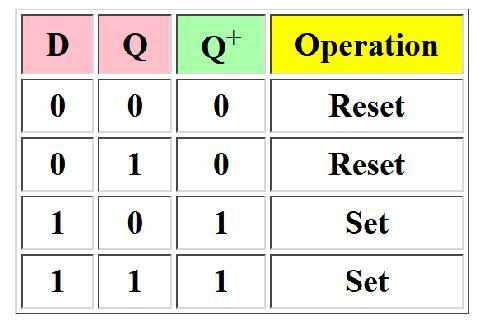
39 5 cents for candy! Watch out no change! Moore machine outputs associated with state Reset N D + Reset Mealy machine outputs associated with transitions Reset/ (N D + Reset)/ [] N D N D / N N/ D 5 [] N D D/ 5 N D / N N/ D [] N D D/ N D / N+D N+D/ 5 [] Reset 5 Reset / 39
40 Example: Moore implementation D D Encode states and map to logic Q D Q Open Q N N N X X X X X X X X X D D Q Q Q present state inputs next state output Q Q D N D D open 4
41 Example: Mealy implementation Reset/ Reset/ N/ D/ 5 N/ D/ N+D/ 5 N D / N D / N D / Reset / Open Q D X X X Q N present state inputs next state output Q Q D N D D open 4
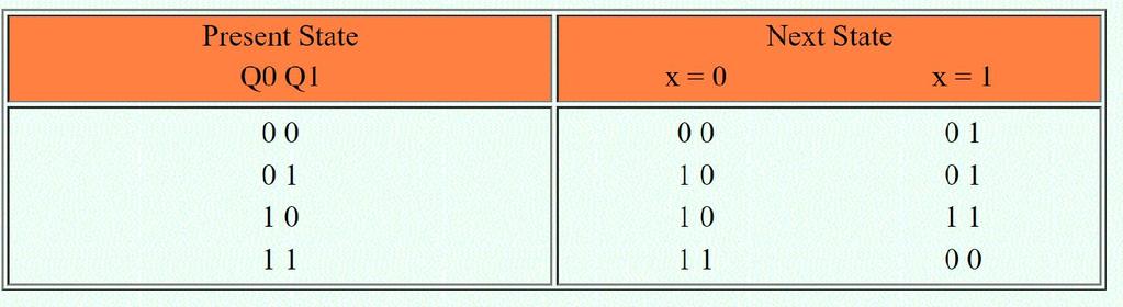
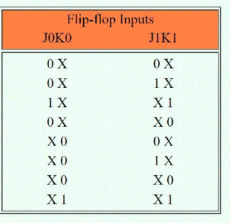
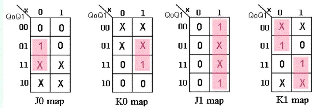
42 FSM design: Multiple input counter Given FSM of a multiple input counter, design the circuit implementing its functionality S S2, S S3 present next state output state S S S S2 S3 S S S3 S S3 S3 S S S S3 S2 S S3 S2 S State Input Inputs State 42
43 Multiple input counter: Logic for D-FF Derive logic equations for inputs of State D-FF Input D II D II 43
44 CSE4: Components and Design Techniques for Digital Systems Register Transfer Level (RTL) Design Slides from Tajana Simunic Rosing
45 High-Level State Machine Some behaviors may be too complex to describe by using classical FSMs Soda dispenser c: bit input, when coin deposited a: 8-bit input: value of the deposited coin s: 8-bit input: cost of a soda d: bit output, processor sets it to when total value of deposited coins equals or exceeds cost of a soda c d 5 s a Soda dispenser processor tot: 5 25
46 Challenges in High-Level State Machines 5.2 Which of the following makes the FSM design of this problem difficult? A. 8-bit input/output B. Tracking the current total C. Multibit comparison D. All of the above E. None of the above c d c d s Soda dispenser processor 5 s a Soda dispenser processor a tot:
47 Benefits of HLSMs s a 8 8 High-level state machine (HLSM) extends FSM with: Multi-bit input/output Local storage Arithmetic operations Conventions Numbers: Single-bit: '' (single quotes) Integer: (no quotes) Multi-bit: (double quotes) == for comparison equal Multi-bit outputs must be registered via local storage // precedes a comment c d Soda dispenser processor Inputs: c (bit), a (8 bits), s (8 bits) Outputs: d (bit) // '' dispenses soda Local storage: tot (8 bits) Init d:='' tot:= SodaDispenser Wait c Add c' (tot<s) tot:=tot+a Disp d:='' 47
48 Benefits of HLSMs s a 8 8 High-level state machine (HLSM) extends FSM with: Multi-bit input/output Local storage Arithmetic operations Conventions Each transition is implicitly ANDed with a rising edge of the clock Any bit output not explicitly assigned a value in a state is implicitly assigned to. This convention does not apply for multibit outputs Every HLSM multibit output is registered c d Soda dispenser processor Inputs: c (bit), a (8 bits), s (8 bits) Outputs: d (bit) // '' dispenses soda Local storage: tot (8 bits) Init d:='' tot:= SodaDispenser Wait c Add c' (tot<s) tot:=tot+a Disp d:='' 48
49 FSMs vs. HLSMs s a 8 8 a How does the HLSM differ from the FSM for this problem? A. The HLSM stores multibit data, but the FSM doesn t B. The FSM stores the state but the HLSM doesn t C. Implementing HLSM and FSM requires multibit data registers D. All of the above E. None of the above c d Soda dispenser processor Inputs: c (bit), a (8 bits), s (8 bits) Outputs: d (bit) // '' dispenses soda Local storage: tot (8 bits) Init d:='' tot:= Wait c Add c *(tot<s) c' (tot<s) tot:=tot+a Disp SodaDispenser d:='' 49
50 Similarities between FSMs & HLSMs s a 8 8 Which of the following are common between HLSMs and FSMs? A. Transitions happen at the edge of a clock B. They both have external complex data C. All of the above D. None of the above c d Soda dispenser processor Inputs: c (bit), a (8 bits), s (8 bits) Outputs: d (bit) // '' dispenses soda Local storage: tot (8 bits) Init d:='' tot:= Wait c Add c *(tot<s) c' (tot<s) tot:=tot+a Disp SodaDispenser d:='' 5
51 RTL Design Process Step : Capture a high-level state machine - Describe the system s desired behavior as a high-level state machine. The state machine consists of states and transitions. The state machine is high level because the transition conditions and the state actions are more than just Boolean operations on single-bit input and outputs Recommendations: - Always list all inputs, outputs and local registers on top of your HLSM diagram - Clearly specify the size in bits of each of them - On states: update the value of registers, update of outputs - On transitions: express conditions in terms of the HLSM inputs or state of the internal values and arithmetic operations between them. 5
52 RTL Design Process Step 2: Convert it to a circuit - 2.a: Create a datapath - Create a datapath to carry out the data operations of the high level state machine - Elements of your datapaths can be registers, adders, comparators, multipliers, dividers, etc. DP control inputs... External data inputs... Datapath... External data outputs 52
53 Datapath components: RTL Design Process clr I A B A B ld reg add cmp Q S lt eq gt I shift<l/r> Q I I mux2x s Q clk^ and clr=: Q= clk^ and ld=: Q=I else Q stays same S = A+B (unsigned) A<B: lt= A=B: eq= A>B: gt= shiftl: << shiftl2: <<2 shiftr: >>... s=: Q=I s=: Q=I A B sub S S = A-B (signed) A B mul P P = A*B (unsigned) A abs Q (signed) Q = A (unsigned) clr inc upcnt Q clk^ and clr=: Q= clk^ and inc=: Q=Q+ else Q stays same W_d W_a W_e R_a R_e R_d RF clk^ and W_e=: RF[W_a]= W_d R_e=: R_d = RF[R_a]
54 RTL Design Process Step 2: Convert it to a circuit - 2.b: Connect the datapath to a controller - Connect the datapath to a controller block. Connect the external control inputs and outputs to the controller block. - Clearly label all control signals that are exchanged between the datapath and the controller External control inputs External control outputs Controller DP control inputs DP control outputs External data inputs... Datapath... External data outputs 54
55 RTL Design Process Step 2: Convert it to a circuit - 2.c: derive the controller s FSM - Convert the high-level state machine to a finite state machine (FSM) for the controller, by replacing data operations with setting and reading of control signals to and from the datapath External control inputs External control outputs Controller DP control inputs DP control outputs External data inputs... Datapath... External data outputs The controller FSM should have: - Inputs: - Ext control inputs - DP control outputs - Outputs: - Ext. control outputs - DP control inputs 55
56 RTL Design Process: summary Capture the behavior with HLSM Convert it to a circuit High-level architecture (datapath and control path) Datapath capable of HLSM's data operations Design controller to control the datapath External control inputs External control outputs Controller DP control inputs DP control outputs External data inputs... Datapath... External data outputs
57 Step 2.a: Create Datapath for Soda Dispenser Need tot register to keep track of the money deposited so far Need 8-bit comparator to compare s (current sum) and a (target cost) Need 8-bit adder to update: tot = tot + a Connect everything Create control IO tot_ld tot_clr s 8 ld clr Inputs: c (bit), a(8 bits), s (8 bits) Outputs : d (bit) Local registers: tot (8 bits) tot Init d= tot= 8 a c 8 Wait (tot<s) c Add c (tot<s) tot= tot+a Disp d= tot_lt_s Datapath 8-bit < 8-bit adder 8
58 Signals in Soda Dispenser Inputs: c (bit), a (8 bits), s (8 bits) Outputs: d (bit) // '' dispenses soda Local storage: tot (8 bits) s a c Add tot_ld tot_clr ld clr tot Init Wait tot:=tot+a a d:='' tot:= SodaDispenser c *(tot<s) c' (tot<s) Disp d:='' tot_lt_s Datapath 8-bit < 8-bit adder 8 According to the current design, under which of the following conditions does the register output tot change at the rising clock edge? A.Whenever the value of the coin inserted ( a ) changes B.Whenever the cost of the soda ( s ) changes C.When the signal tot_ld becomes high D.When the signal tot_clr becomes high E.Both C. & D. a
59 Step 2.b: Connect Datapath to a Controller s a Controller s inputs External input c (coin detected) Input from datapath comparator s c output, which we named tot_lt_s Controller s outputs External output d (dispense soda) Outputs to datapath to load and clear the tot register d Controller tot_ld tot_clr tot_lt_s s a 8 8 Datapath tot_ld tot_clr tot_lt_s 8 Datapath ld clr 8-bit < tot 8 8-bit adder 8 8
60 Step 2.c Derive the Controller s FSM FSM has the same states and arcs as HLSM Replace all references to the data elements in the HLSM with appropriate control signals & values c d Controller tot_ld tot_clr tot_lt_s s a 8 8 Datapath s a c d Inputs: :c,tot_lt_s(bit) Outputs:d,tot_ld,tot_clr(bit) Init d= tot_clr= Wait c Add tot_ld= c * tot_lt_s Disp tot_ld tot_clr tot_lt_s tot_ld tot_clr tot_lt_s 8 ld clr 8-bit < Datapath tpt 8 8-bit adder 8 8 Controller d=
61 Final Step: Implement the controller FSM Implement the FSM as a state register and logic I n p u t s : : c, tot_lt_s (bit) s s c tot_lt_s n n d tot_ld tot_clr Outputs: d, tot_ld, tot_clr (bit) c d Init d= tot_clr= Wait c Add tot_ld= c * tot_lt_s Disp tot_ld tot_clr tot_lt_s Init Wait Add Controller d= Disp
62 Another RTL Design: Laser-Based Distance Measurer T (in seconds) laser sensor D 2D = T sec * 3* 8 m/sec Object of interest Laser-based distance measurement pulse laser, measure time T to sense reflection Laser light travels at speed of light, 3* 8 m/sec Distance is thus D = T sec * 3* 8 m/sec / 2
63 Laser-Based Distance Measurer IO T (in seconds) laser B from button L to laser sensor D to display 6 Laser-based distance measurer S from sensor Inputs/outputs B: bit input, from button, to begin measurement L: bit output, activates laser S: bit input, senses laser reflection D: 6-bit output, to display computed distance 63
64 Laser-Based Distance Measurer: HLSM DistanceMeasurer Inputs: B (bit), S (bit) Outputs: L (bit), D (6 bits) Local storage: Dreg(6) from button B D to display 6 Laserbased distance measurer L to laser S from sensor a S? L := '' // laser off Dreg := // distance is (first state usually initializes the system) Declare inputs, outputs, and local storage Dreg required for multi-bit output Create initial state, name it S Initialize laser to off (L:='') Initialize displayed distance to (Dreg:=) Recall: '' means single bit, means integer 64
65 Laser-Based Distance Measurer: HLSM DistanceMeasurer... B' // button not pressed from button B D to display 6 Laserbased distance measurer L to laser S from sensor S L := '' Dreg := S B? // button pressed Add another state, S, that waits for a button press B' stay in S, keep waiting B go to a new state S2 65
66 Laser-Based Distance Measurer: HLSM DistanceMeasurer... B' from button B D to display 6 Laserbased distance measurer L to laser S from sensor S S B S2 S3 L := '' Dreg := L := '' // laser on L := '' // laser off Add a state S2 that turns on the laser (L:='') Then turn off laser (L:='') in a state S3 66
67 Laser-Based Distance Measurer: HLSM DistanceMeasurer Inputs: B (bit), S (bit) Outputs: L (bit), D (6 bits) Local storage: Dreg, Dctr (6 bits) B' S' // no reflection B from button D to display 6 Laser-based distance measurer L to laser S from sensor S S S2 S3 B L := '' Dreg := Dctr := // reset cycle count L := '' L := '' Dctr := Dctr + // count cycles S // reflection? a Stay in S3 until sense reflection (S) To measure time, count cycles while in S3 To count, declare local storage Dctr Initialize Dctr to in S. In S2 would have been O.K. too. Don't forget to initialize local storage common mistake Increment Dctr each cycle in S3 67
68 Laser-Based Distance Measurer: HLSM DistanceMeasurer Inputs: B (bit), S (bit) Outputs: L (bit), D (6 bits) Local storage: Dreg, Dctr (6 bits) B' S' B from button D to display 6 Laserbased distance measurer L to laser S from sensor S S S2 S3 B L := '' Dreg := Dctr := L := '' S L := '' Dctr := Dctr+ S4 Dreg := Dctr/2 // calculate D a Once reflection detected (S), go to new state S4 Calculate distance Assuming clock frequency is 3x 8, Dctr holds number of meters, so Dreg:=Dctr/2 After S4, go back to S to wait for button again 68
69 Laser-Based Distance Measurer: Create a Datapath DistanceMeasurer Inputs: B (bit), S (bit) Outputs: L (bit), D (6 bits) Local storage: Dreg, Dctr (6 bits) B' S' S S S2 S3 B L := '' Dreg := Dctr := L := '' S L := '' Dctr := Dctr+ S4 Dreg := Dctr/2 // calculate D 6 Datapath HLSM data I/O DP I/O HLSM local storage reg HLSM state action and transition condition data computation Datapath components and connections Dreg_clr Dreg_ld Dctr_clr Dctr_ld A B Add: add(6) S 6 clr I ld Dctr: reg(6) Q 6 I Shr: shiftr(6) Q 6 clr ld I Dreg: reg(6) Q D 6 69
70 Laser-Based Distance Measure: Connecting the Datapath to a Controller from button B Controller Dreg_clr L S to laser from sensor Dreg_ld Dctr_clr Datapath to display D 6 3 MHz Clock Dctr_ld 7
71 DistanceMeasurer Laser-Based Distance Measurer: Derive the Controller FSM S S S2 S3 B L := '' Dreg := B' Inputs: B (bit), S (bit) Outputs: L (bit), D (6 bits) Local storage: Dreg, Dctr (6 bits) Dctr := HLSM L := '' S' S L := '' Dctr := Dctr+ S4 Dreg := Dctr/2 // calculate D Dreg_clr Dreg_ld Dctr_clr Dctr_ld D clr ld 6 A B Add: add(6) S 6 I Dctr: reg(6) Q 6 Datapath I Shr: shiftr(6) Q 6 clr I ld Dreg: reg(6) Q 6 FSM has same states, transitions, and control I/O Achieve each HLSM data operation using datapath control signals in FSM Controller B Inputs: B, S B S S S2 S3 L = L = L = L = Dreg_clr = Dreg_clr = Dreg_ld = Dreg_ld = Dctr_clr = Dctr_clr = Dctr_ld = Dctr_ld = (clear count) (laser on) Dreg_clr = Dreg_ld = Dctr_clr = Dctr_ld = (laser off) (clear Dreg) Outputs: L, Dreg_clr, Dreg_ld, Dctr_clr, Dctr_ld S S Dreg_clr = Dreg_ld = Dctr_clr = Dctr_ld = (laser off) (count up) S4 L = Dreg_clr = Dreg_ld = Dctr_clr = Dctr_ld = (load Dreg with Dctr/2) (stop counting) 7
72 Laser-Based Distance Measurer: Simplify the Controller FSM Controller Inputs: B, S Outputs: L, Dreg_clr, Dreg_ld, Dctr_clr, Dctr_ld B S B S S S2 S3 L = Dctr_clr = L = L = Dreg_clr = (clear count) (laser on) Dctr_ld = (laser off) (laser off) (clear Dreg) (count up) S S4 Dreg_ld = Dctr_ld = (load Dreg with Dctr/2) (stop counting) Same FSM, using convention of unassigned outputs implicitly assigned Some assignments to still shown, due to their importance in understanding desired controller behavior 72
Timing Constraints in Sequential Designs. 63 Sources: TSR, Katz, Boriello & Vahid
 Timing Constraints in Sequential esigns 63 Sources: TSR, Katz, Boriello & Vahid Where we are now. What we covered last time: FSMs What we ll do next: Timing constraints Upcoming deadlines: ZyBook today:
ALU, Latches and Flip-Flops
 CSE14: Components and Design Techniques for Digital Systems ALU, Latches and Flip-Flops Tajana Simunic Rosing Where we are. Last time: ALUs Plan for today: ALU example, latches and flip flops Exam #1 grades
Register Transfer Level (RTL) Design based on Vahid chap. 5
 Design based on Vahid chap. 5") CSE4: Components and Design Techniques for Digital Systems Register Transfer Level (RTL) Design based on Vahid chap. 5 Tajana Simunic Rosing RTL Design Method RTL Design example: Laser-Based Distance Measurer
CSE4: Components and Design Techniques for Digital Systems Register Transfer Level (RTL) Design based on Vahid chap. 5 Tajana Simunic Rosing RTL Design Method RTL Design example: Laser-Based Distance Measurer
Lecture 10: Sequential Networks: Timing and Retiming
 Lecture 10: Sequential Networks: Timing and Retiming CSE 140: Components and Design Techniques for Digital Systems Diba Mirza Dept. of Computer Science and Engineering University of California, San Diego
Homework #4. CSE 140 Summer Session Instructor: Mohsen Imani. Only a subset of questions will be graded
 Homework #4 CSE 140 Summer Session 2 2017 Instructor: Mohsen Imani Only a subset of questions will be graded 1) For the circuit shown below, do the following: a. Write a logic equation for the output P
Review for Final Exam
 CSE140: Components and Design Techniques for Digital Systems Review for Final Exam Mohsen Imani CAPE Please submit your evaluations!!!! RTL design Use the RTL design process to design a system that has
CSE 140 Midterm 3 version A Tajana Simunic Rosing Spring 2015
 CSE 140 Midterm 3 version A Tajana Simunic Rosing Spring 2015 Name of the person on your left : Name of the person on your right: 1. 20 points 2. 20 points 3. 20 points 4. 15 points 5. 15 points 6. 10
Chapter 3. Digital Design and Computer Architecture, 2 nd Edition. David Money Harris and Sarah L. Harris. Chapter 3 <1>
 Chapter 3 Digital Design and Computer Architecture, 2 nd Edition David Money Harris and Sarah L. Harris Chapter 3 Chapter 3 :: Topics Introduction Latches and Flip-Flops Synchronous Logic Design Finite
Problem Set 9 Solutions
 CSE 26 Digital Computers: Organization and Logical Design - 27 Jon Turner Problem Set 9 Solutions. For each of the sequential circuits shown below, draw in the missing parts of the timing diagrams. You
CSE 140 Midterm 2 - Solutions Prof. Tajana Simunic Rosing Spring 2013
 CSE 140 Midterm 2 - Solutions Prof. Tajana Simunic Rosing Spring 2013 Do not start the exam until you are told. Write your name and PID at the top of every page. Do not separate the pages. Turn off and
Chapter 3. Chapter 3 :: Topics. Introduction. Sequential Circuits
 Chapter 3 Chapter 3 :: Topics igital esign and Computer Architecture, 2 nd Edition avid Money Harris and Sarah L. Harris Introduction Latches and Flip Flops Synchronous Logic esign Finite State Machines
EEE2135 Digital Logic Design
 EEE2135 Digital Logic Design Chapter 7. Sequential Circuits Design 서강대학교 전자공학과 1. Model of Sequential Circuits 1) Sequential vs. Combinational Circuits a. Sequential circuits: Outputs depend on both the
CPE100: Digital Logic Design I
 Chapter 3 Professor Brendan Morris, SEB 3216, brendan.morris@unlv.edu http://www.ee.unlv.edu/~b1morris/cpe1/ CPE1: Digital Logic Design I Section 14: Dr. Morris Sequential Logic Design Chapter 3 Chapter
CSE 140 Midterm 2 Tajana Simunic Rosing. Spring 2008
 CSE 14 Midterm 2 Tajana Simunic Rosing Spring 28 Do not start the exam until you are told to. Turn off any cell phones or pagers. Write your name and PID at the top of every page. Do not separate the pages.
Different encodings generate different circuits
 FSM State Encoding Different encodings generate different circuits no easy way to find best encoding with fewest logic gates or shortest propagation delay. Binary encoding: K states need log 2 K bits i.e.,
CSE140: Components and Design Techniques for Digital Systems. Midterm Information. Instructor: Mohsen Imani. Sources: TSR, Katz, Boriello & Vahid
 CSE140: Components and Design Techniques for Digital Systems Midterm Information Instructor: Mohsen Imani Midterm Topics In general: everything that was covered in homework 1 and 2 and related lectures,
Adders, subtractors comparators, multipliers and other ALU elements
 CSE4: Components and Design Techniques for Digital Systems Adders, subtractors comparators, multipliers and other ALU elements Instructor: Mohsen Imani UC San Diego Slides from: Prof.Tajana Simunic Rosing
Sequential Logic Worksheet
 Sequential Logic Worksheet Concept Inventory: Notes: D-latch & the Dynamic Discipline D-register Timing constraints for sequential circuits Set-up and hold times for sequential circuits 6.004 Worksheet
ECEN 248: INTRODUCTION TO DIGITAL SYSTEMS DESIGN. Week 9 Dr. Srinivas Shakkottai Dept. of Electrical and Computer Engineering
 ECEN 248: INTRODUCTION TO DIGITAL SYSTEMS DESIGN Week 9 Dr. Srinivas Shakkottai Dept. of Electrical and Computer Engineering TIMING ANALYSIS Overview Circuits do not respond instantaneously to input changes
Synchronous Sequential Circuit Design. Digital Computer Design
 Synchronous Sequential Circuit Design Digital Computer Design Races and Instability Combinational logic has no cyclic paths and no races If inputs are applied to combinational logic, the outputs will always
Design of Sequential Circuits
 Design of Sequential Circuits Seven Steps: Construct a state diagram (showing contents of flip flop and inputs with next state) Assign letter variables to each flip flop and each input and output variable
Latches. October 13, 2003 Latches 1
 Latches The second part of CS231 focuses on sequential circuits, where we add memory to the hardware that we ve already seen. Our schedule will be very similar to before: We first show how primitive memory
Synchronous Sequential Circuit Design. Dr. Ehab A. H. AL-Hialy Page 1
 Synchronous Sequential Circuit Design Dr. Ehab A. H. AL-Hialy Page Motivation Analysis of a few simple circuits Generalizes to Synchronous Sequential Circuits (SSC) Outputs are Function of State (and Inputs)
CPE100: Digital Logic Design I
 Professor Brendan Morris, SEB 3216, brendan.morris@unlv.edu CPE100: Digital Logic Design I Final Review http://www.ee.unlv.edu/~b1morris/cpe100/ 2 Logistics Tuesday Dec 12 th 13:00-15:00 (1-3pm) 2 hour
CSE140: Digital Logic Design Registers and Counters
 CSE14: Digital Logic Design Registers and Counters Prof. Tajana Simunic Rosing 38 Where we are now. What we covered last time: ALUs, SR Latch Latches and FlipFlops (FFs) Registers What we ll do next FSMs
Ch 7. Finite State Machines. VII - Finite State Machines Contemporary Logic Design 1
 Ch 7. Finite State Machines VII - Finite State Machines Contemporary Logic esign 1 Finite State Machines Sequential circuits primitive sequential elements combinational logic Models for representing sequential
EECS Components and Design Techniques for Digital Systems. FSMs 9/11/2007
 EECS 150 - Components and Design Techniques for Digital Systems FSMs 9/11/2007 Sarah Bird Electrical Engineering and Computer Sciences University of California, Berkeley Slides borrowed from David Culler
Total time is: 1 setup, 2 AND, 3 XOR, 1 delay = (1*1) + (2*2) + (3*3) + (1*1) = 15ns
 + (2*2) + (3*3) + (1*1) = 15ns") Clock Period/ Delay Analysis: Find longest possible path (time-wise) between two flip-flops. If 2ns for AND and 3ns for XOR, with T delayff = 1ns and T setupff = 1 ns. So the total time is: 1 setupff +
Clock Period/ Delay Analysis: Find longest possible path (time-wise) between two flip-flops. If 2ns for AND and 3ns for XOR, with T delayff = 1ns and T setupff = 1 ns. So the total time is: 1 setupff +
Adders, subtractors comparators, multipliers and other ALU elements
 CSE4: Components and Design Techniques for Digital Systems Adders, subtractors comparators, multipliers and other ALU elements Adders 2 Circuit Delay Transistors have instrinsic resistance and capacitance
ENGG 1203 Tutorial _03 Laboratory 3 Build a ball counter. Lab 3. Lab 3 Gate Timing. Lab 3 Steps in designing a State Machine. Timing diagram of a DFF
 ENGG 1203 Tutorial _03 Laboratory 3 Build a ball counter Timing diagram of a DFF Lab 3 Gate Timing difference timing for difference kind of gate, cost dependence (1) Setup Time = t2-t1 (2) Propagation
Finite State Machine (FSM)
") Finite State Machine (FSM) Consists of: State register Stores current state Loads next state at clock edge Combinational logic Computes the next state Computes the outputs S S Next State CLK Current State
Finite State Machine (FSM) Consists of: State register Stores current state Loads next state at clock edge Combinational logic Computes the next state Computes the outputs S S Next State CLK Current State
King Fahd University of Petroleum and Minerals College of Computer Science and Engineering Computer Engineering Department
 King Fahd University of Petroleum and Minerals College of Computer Science and Engineering Computer Engineering Department Page 1 of 13 COE 202: Digital Logic Design (3-0-3) Term 112 (Spring 2012) Final
Lecture 10: Synchronous Sequential Circuits Design
 Lecture 0: Synchronous Sequential Circuits Design. General Form Input Combinational Flip-flops Combinational Output Circuit Circuit Clock.. Moore type has outputs dependent only on the state, e.g. ripple
Appendix B. Review of Digital Logic. Baback Izadi Division of Engineering Programs
 Appendix B Review of Digital Logic Baback Izadi Division of Engineering Programs bai@engr.newpaltz.edu Elect. & Comp. Eng. 2 DeMorgan Symbols NAND (A.B) = A +B NOR (A+B) = A.B AND A.B = A.B = (A +B ) OR
Stop Watch (System Controller Approach)
") Stop Watch (System Controller Approach) Problem Design a stop watch that can measure times taken for two events Inputs CLK = 6 Hz RESET: Asynchronously reset everything X: comes from push button First
Stop Watch (System Controller Approach) Problem Design a stop watch that can measure times taken for two events Inputs CLK = 6 Hz RESET: Asynchronously reset everything X: comes from push button First
14.1. Unit 14. State Machine Design
 4. Unit 4 State Machine Design 4.2 Outcomes I can create a state diagram to solve a sequential problem I can implement a working state machine given a state diagram STATE MACHINES OVERVIEW 4.3 4.4 Review
Sequential Circuits. Circuits with state. Silvina Hanono Wachman Computer Science & Artificial Intelligence Lab M.I.T. L06-1
 Sequential Circuits Circuits with state Silvina Hanono Wachman Computer Science & Artificial Intelligence Lab M.I.T. L06-1 Combinational circuits A 0 A 1 A n-1. Sel lg(n) O Mux A B Comparator Result: LT,
Counters. We ll look at different kinds of counters and discuss how to build them
 Counters We ll look at different kinds of counters and discuss how to build them These are not only examples of sequential analysis and design, but also real devices used in larger circuits 1 Introducing
Sequential Circuit Design
 Sequential Circuit esign esign Procedure. Specification 2. Formulation Obtain a state diagram or state table 3. State Assignment Assign binary codes to the states 4. Flip-Flop Input Equation etermination
University of Toronto Faculty of Applied Science and Engineering Edward S. Rogers Sr. Department of Electrical and Computer Engineering
 University of Toronto Faculty of Applied Science and Engineering Edward S. Rogers Sr. Department of Electrical and Computer Engineering Final Examination ECE 241F - Digital Systems Examiners: S. Brown,
Fundamentals of Digital Design
 Fundamentals of Digital Design Digital Radiation Measurement and Spectroscopy NE/RHP 537 1 Binary Number System The binary numeral system, or base-2 number system, is a numeral system that represents numeric
Models for representing sequential circuits
 Sequential Circuits Models for representing sequential circuits Finite-state machines (Moore and Mealy) Representation of memory (states) Changes in state (transitions) Design procedure State diagrams
CS221: Digital Design. Dr. A. Sahu. Indian Institute of Technology Guwahati
 CS221: Digital Design Counter&Registers Dr. A. Sahu DeptofComp.Sc.&Engg. Indian Institute of Technology Guwahati Outline Counter : Synchronous Vs Asynchronous Counter: Finite it State t Machine Mhi A register
Digital Logic and Design (Course Code: EE222) Lecture 19: Sequential Circuits Contd..
 Lecture 19: Sequential Circuits Contd..") Indian Institute of Technology Jodhpur, Year 2017-2018 Digital Logic and Design (Course Code: EE222) Lecture 19: Sequential Circuits Contd.. Course Instructor: Shree Prakash Tiwari Email: sptiwari@iitj.ac.in
Indian Institute of Technology Jodhpur, Year 2017-2018 Digital Logic and Design (Course Code: EE222) Lecture 19: Sequential Circuits Contd.. Course Instructor: Shree Prakash Tiwari Email: sptiwari@iitj.ac.in
10/12/2016. An FSM with No Inputs Moves from State to State. ECE 120: Introduction to Computing. Eventually, the States Form a Loop
 University of Illinois at Urbana-Champaign Dept. of Electrical and Computer Engineering An FSM with No Inputs Moves from State to State What happens if an FSM has no inputs? ECE 120: Introduction to Computing
Digital Design. Sequential Logic
 Principles Of igital esign Chapter 6 Sequential Logic Chapter preview Boolean algebra 3 Logic gates and flip-flops 3 Finite-state machine 6 Logic design techniques 4 Sequential design techniques 6 Binary
Sequential logic and design
 Principles Of Digital Design Sequential logic and design Analysis State-based (Moore) Input-based (Mealy) FSM definition Synthesis State minimization Encoding Optimization and timing Copyright 20-20by
Fundamentals of Computer Systems
 Fundamentals of Computer Systems Review for the Midterm Stephen A. Edwards Columbia University Spring 22 The Midterm 75 minutes 4 5 problems Closed book Simple calculators are OK, but unnecessary One double-sided
King Fahd University of Petroleum and Minerals College of Computer Science and Engineering Computer Engineering Department
 King Fahd University of Petroleum and Minerals College of Computer Science and Engineering Computer Engineering Department Page of COE 22: Digital Logic Design (3--3) Term (Fall 22) Final Exam Sunday January
Sequential Logic Design: Controllers
 Sequential Logic Design: Controllers Controller Design, Flip Flop Timing Copyright (c) 2012 Sean Key Standard Controller Architecture Controller A circuit that implements a FSM is referred to as a controller
Fundamentals of Computer Systems
 Fundamentals of Computer Systems Review for the Final Stephen A. Edwards Columbia University Summer 25 The Final 2 hours 8 problems Closed book Simple calculators are OK, but unnecessary One double-sided
Chapter 5. Digital Design and Computer Architecture, 2 nd Edition. David Money Harris and Sarah L. Harris. Chapter 5 <1>
 Chapter 5 Digital Design and Computer Architecture, 2 nd Edition David Money Harris and Sarah L. Harris Chapter 5 Chapter 5 :: Topics Introduction Arithmetic Circuits umber Systems Sequential Building
Example: vending machine
 Example: vending machine Release item after 15 cents are deposited Single coin slot for dimes, nickels o change Reset Coin Sensor Vending Machine FSM Open Release Mechanism Clock Spring 2005 CSE370 - guest
Parity Checker Example. EECS150 - Digital Design Lecture 9 - Finite State Machines 1. Formal Design Process. Formal Design Process
 Parity Checker Example A string of bits has even parity if the number of 1 s in the string is even. Design a circuit that accepts a bit-serial stream of bits and outputs a 0 if the parity thus far is even
ECEN 248: INTRODUCTION TO DIGITAL SYSTEMS DESIGN. Week 7 Dr. Srinivas Shakkottai Dept. of Electrical and Computer Engineering
 ECEN 248: INTRODUCTION TO DIGITAL SYSTEMS DESIGN Week 7 Dr. Srinivas Shakkottai Dept. of Electrical and Computer Engineering SEQUENTIAL CIRCUITS: LATCHES Overview Circuits require memory to store intermediate
State and Finite State Machines
 State and Finite State Machines See P&H Appendix C.7. C.8, C.10, C.11 Hakim Weatherspoon CS 3410, Spring 2013 Computer Science Cornell University Big Picture: Building a Processor memory inst register
3. Complete the following table of equivalent values. Use binary numbers with a sign bit and 7 bits for the value
 EGC22 Digital Logic Fundamental Additional Practice Problems. Complete the following table of equivalent values. Binary. Octal 35.77 33.23.875 29.99 27 9 64 Hexadecimal B.3 D.FD B.4C 2. Calculate the following
Sequential Circuits Sequential circuits combinational circuits state gate delay
 Sequential Circuits Sequential circuits are those with memory, also called feedback. In this, they differ from combinational circuits, which have no memory. The stable output of a combinational circuit
Lecture 8: Sequential Networks and Finite State Machines
 Lecture 8: Sequential Networks and Finite State Machines CSE 140: Components and Design Techniques for Digital Systems Spring 2014 CK Cheng, Diba Mirza Dept. of Computer Science and Engineering University
CSC 322: Computer Organization Lab
 CSC 322: Computer Organization Lab Lecture 3: Logic Design Dr. Haidar M. Harmanani CSC 322: Computer Organization Lab Part I: Combinational Logic Dr. Haidar M. Harmanani Logical Design of Digital Systems
Review: Designing with FSM. EECS Components and Design Techniques for Digital Systems. Lec09 Counters Outline.
 Review: Designing with FSM EECS 150 - Components and Design Techniques for Digital Systems Lec09 Counters 9-28-04 David Culler Electrical Engineering and Computer Sciences University of California, Berkeley
Logic Design II (17.342) Spring Lecture Outline
 Spring Lecture Outline") Logic Design II (17.342) Spring 2012 Lecture Outline Class # 10 April 12, 2012 Dohn Bowden 1 Today s Lecture First half of the class Circuits for Arithmetic Operations Chapter 18 Should finish at least
Logic Design II (17.342) Spring 2012 Lecture Outline Class # 10 April 12, 2012 Dohn Bowden 1 Today s Lecture First half of the class Circuits for Arithmetic Operations Chapter 18 Should finish at least
CSE 140: Components and Design Techniques for Digital Systems. Lecture 9: Sequential Networks: Implementation
 CSE 4: Components and Design Techniques for Digital Systems Lecture 9: Sequential Networks: Implementation CK Cheng Dept. of Computer Science and Engineering University of California, San Diego Implementation
Lecture 13: Sequential Circuits, FSM
 Lecture 13: Sequential Circuits, FSM Today s topics: Sequential circuits Finite state machines 1 Clocks A microprocessor is composed of many different circuits that are operating simultaneously if each
課程名稱 : 數位邏輯設計 P-1/ /6/11
 課程名稱 : 數位邏輯設計 P-1/55 2012/6/11 Textbook: Digital Design, 4 th. Edition M. Morris Mano and Michael D. Ciletti Prentice-Hall, Inc. 教師 : 蘇慶龍 INSTRUCTOR : CHING-LUNG SU E-mail: kevinsu@yuntech.edu.tw Chapter
EE 209 Logic Cumulative Exam Name:
 EE 209 Logic Cumulative Exam Name: 1.) Answer the following questions as True or False a.) A 4-to-1 multiplexer requires at least 4 select lines: true / false b.) An 8-to-1 mux and no other logi can be
CprE 281: Digital Logic
 CprE 28: Digital Logic Instructor: Alexander Stoytchev http://www.ece.iastate.edu/~alexs/classes/ Simple Processor CprE 28: Digital Logic Iowa State University, Ames, IA Copyright Alexander Stoytchev Digital
Synchronous Sequential Logic
 1 IT 201 DIGITAL SYSTEMS DESIGN MODULE4 NOTES Synchronous Sequential Logic Sequential Circuits - A sequential circuit consists of a combinational circuit and a feedback through the storage elements in
UNIVERSITY OF BOLTON SCHOOL OF ENGINEERING BENG (HONS) ELECTRICAL & ELECTRONICS ENGINEERING EXAMINATION SEMESTER /2017
 ELECTRICAL & ELECTRONICS ENGINEERING EXAMINATION SEMESTER /2017") UNIVERSITY OF BOLTON TW35 SCHOOL OF ENGINEERING BENG (HONS) ELECTRICAL & ELECTRONICS ENGINEERING EXAMINATION SEMESTER 2-2016/2017 INTERMEDIATE DIGITAL ELECTRONICS AND COMMUNICATIONS MODULE NO: EEE5002
UNIVERSITY OF BOLTON TW35 SCHOOL OF ENGINEERING BENG (HONS) ELECTRICAL & ELECTRONICS ENGINEERING EXAMINATION SEMESTER 2-2016/2017 INTERMEDIATE DIGITAL ELECTRONICS AND COMMUNICATIONS MODULE NO: EEE5002
CprE 281: Digital Logic
 CprE 281: Digital Logic Instructor: Alexander Stoytchev http://www.ece.iastate.edu/~alexs/classes/ Synchronous Sequential Circuits Basic Design Steps CprE 281: Digital Logic Iowa State University, Ames,
ELEC Digital Logic Circuits Fall 2014 Sequential Circuits (Chapter 6) Finite State Machines (Ch. 7-10)
 Finite State Machines (Ch. 7-10)") ELEC 2200-002 Digital Logic Circuits Fall 2014 Sequential Circuits (Chapter 6) Finite State Machines (Ch. 7-10) Vishwani D. Agrawal James J. Danaher Professor Department of Electrical and Computer Engineering
ELEC 2200-002 Digital Logic Circuits Fall 2014 Sequential Circuits (Chapter 6) Finite State Machines (Ch. 7-10) Vishwani D. Agrawal James J. Danaher Professor Department of Electrical and Computer Engineering
Introduction EE 224: INTRODUCTION TO DIGITAL CIRCUITS & COMPUTER DESIGN. Lecture 6: Sequential Logic 3 Registers & Counters 5/9/2010
 EE 224: INTROUCTION TO IGITAL CIRCUITS & COMPUTER ESIGN Lecture 6: Sequential Logic 3 Registers & Counters 05/10/2010 Avinash Kodi, kodi@ohio.edu Introduction 2 A Flip-Flop stores one bit of information
Week-5. Sequential Circuit Design. Acknowledgement: Most of the following slides are adapted from Prof. Kale's slides at UIUC, USA.
 Week-5 Sequential Circuit Design Acknowledgement: Most of the following slides are adapted from Prof. Kale's slides at UIUC, USA. Storing a value: SR = 00 What if S = 0 and R = 0? The equations on the
EXPERIMENT Bit Binary Sequential Multiplier
 12.1 Objectives EXPERIMENT 12 12. -Bit Binary Sequential Multiplier Introduction of large digital system design, i.e. data path and control path. To apply the above concepts to the design of a sequential
ECE/Comp Sci 352 Digital Systems Fundamentals. Charles R. Kime Section 2 Fall Logic and Computer Design Fundamentals
 University of Wisconsin - Madison ECE/Comp Sci 352 Digital Systems Fundamentals Charles R. Kime Section 2 Fall 2001 Lecture 5 Registers & Counters Part 2 Charles Kime Counters Counters are sequential circuits
Design at the Register Transfer Level
 Week-7 Design at the Register Transfer Level Algorithmic State Machines Algorithmic State Machine (ASM) q Our design methodologies do not scale well to real-world problems. q 232 - Logic Design / Algorithmic
University of Toronto Faculty of Applied Science and Engineering Edward S. Rogers Sr. Department of Electrical and Computer Engineering
 University of Toronto Faculty of Applied Science and Engineering Edward S. Rogers Sr. Department of Electrical and Computer Engineering Final Examination ECE 241F - Digital Systems Examiners: J. Rose and
Synchronous Sequential Circuit Design
 Synchronous Sequential Circuit Design 1 Sequential circuit design In sequential circuit design, we turn some description into a working circuit We first make a state table or diagram to express the computation
EET 310 Flip-Flops 11/17/2011 1
 EET 310 Flip-Flops 11/17/2011 1 FF s and some Definitions Clock Input: FF s are controlled by a trigger or Clock signal. All FF s have a clock input. If a device which attempts to do a FF s task does not
5. Sequential Logic x Computation Structures Part 1 Digital Circuits. Copyright 2015 MIT EECS
 5. Sequential Logic 6.004x Computation Structures Part 1 igital Circuits Copyright 2015 MIT EECS 6.004 Computation Structures L5: Sequential Logic, Slide #1 Something We Can t Build (Yet) What if you were
ENGG 1203 Tutorial. Solution (b) Solution (a) Simplification using K-map. Combinational Logic (II) and Sequential Logic (I) 8 Feb Learning Objectives
 Solution (a) Simplification using K-map. Combinational Logic (II) and Sequential Logic (I) 8 Feb Learning Objectives") ENGG 23 Tutorial Simplification using K-map Combinational Logic (II) and Sequential Logic (I) 8 Feb Learning Objectives Apply Karnaugh map for logic simplification Design a finite state machine News HW
ENGG 23 Tutorial Simplification using K-map Combinational Logic (II) and Sequential Logic (I) 8 Feb Learning Objectives Apply Karnaugh map for logic simplification Design a finite state machine News HW
EECS150 - Digital Design Lecture 23 - FSMs & Counters
 EECS150 - Digital Design Lecture 23 - FSMs & Counters April 8, 2010 John Wawrzynek Spring 2010 EECS150 - Lec22-counters Page 1 One-hot encoding of states. One FF per state. State Encoding Why one-hot encoding?
Register Transfer Level
 Register Transfer Level CSE3201 RTL A digital system is represented at the register transfer level by these three components 1. The set of registers in the system 2. The operation that are performed on
11.1 As mentioned in Experiment 10, sequential logic circuits are a type of logic circuit where the output of
 EE 2449 Experiment 11 Jack Levine and Nancy Warter-Perez CALIFORNIA STATE UNIVERSITY LOS ANGELES Department of Electrical and Computer Engineering EE-2449 Digital Logic Lab EXPERIMENT 11 SEQUENTIAL CIRCUITS
Topic 8: Sequential Circuits
 Topic 8: Sequential Circuits Readings : Patterson & Hennesy, Appendix B.4 - B.6 Goals Basic Principles behind Memory Elements Clocks Applications of sequential circuits Introduction to the concept of the
Digital Electronics Sequential Logic
 /5/27 igital Electronics Sequential Logic r. I. J. Wassell Sequential Logic The logic circuits discussed previously are known as combinational, in that the output depends only on the condition of the latest
CPE/EE 422/522. Chapter 1 - Review of Logic Design Fundamentals. Dr. Rhonda Kay Gaede UAH. 1.1 Combinational Logic
 CPE/EE 422/522 Chapter - Review of Logic Design Fundamentals Dr. Rhonda Kay Gaede UAH UAH Chapter CPE/EE 422/522. Combinational Logic Combinational Logic has no control inputs. When the inputs to a combinational
ELCT201: DIGITAL LOGIC DESIGN
 ELCT201: DIGITAL LOGIC DESIGN Dr. Eng. Haitham Omran, haitham.omran@guc.edu.eg Dr. Eng. Wassim Alexan, wassim.joseph@guc.edu.eg Following the slides of Dr. Ahmed H. Madian Lecture 10 محرم 1439 ه Winter
ENEL Digital Circuits Final Examination
 Name: I#: Lecture Section: ENEL 353 - igital Circuits Final Examination Lecture sections : N. R. Bartley, MWF : :5, ENC 24 2: S. A. Norman, MWF : :5, ST 45 Wednesday, ecember 7, 24 Time: 7: PM : PM Locations:
CSE140L: Components and Design Techniques for Digital Systems Lab. FSMs. Instructor: Mohsen Imani. Slides from Tajana Simunic Rosing
 CSE140L: Components and Design Techniques for Digital Systems Lab FSMs Instructor: Mohsen Imani Slides from Tajana Simunic Rosing Source: Vahid, Katz 1 FSM design example Moore vs. Mealy Remove one 1 from
Generalized FSM model: Moore and Mealy
 Lecture 18 Logistics HW7 is due on Monday (and topic included in midterm 2) Midterm 2 on Wednesday in lecture slot cover materials up to today s lecture Review session Tuesday 4:15pm in EEB125 Last lecture
Review: Designing with FSM. EECS Components and Design Techniques for Digital Systems. Lec 09 Counters Outline.
 Review: esigning with FSM EECS 150 - Components and esign Techniques for igital Systems Lec 09 Counters 9-28-0 avid Culler Electrical Engineering and Computer Sciences University of California, Berkeley
COE 202: Digital Logic Design Sequential Circuits Part 3. Dr. Ahmad Almulhem ahmadsm AT kfupm Phone: Office:
 COE 202: Digital Logic Design Sequential Circuits Part 3 Dr. Ahmad Almulhem Email: ahmadsm AT kfupm Phone: 860-7554 Office: 22-324 Objectives State Reduction and Assignment Design of Synchronous Sequential
or 0101 Machine
 Synchronous State Graph or Synchronous State Graph or Detector Design a state graph for a machine with: One input X, one output Z. Z= after receiving the complete sequence or Overlapped sequences are detected.
Lecture 9: Sequential Logic Circuits. Reading: CH 7
 Lecture 9: Sequential Logic Circuits Reading: CH 7 Sequential Logic FSM (Finite-state machine) Inputs Current State COMBINATIONAL LOGIC Registers Outputs = f(current, inputs) Next state 2 storage mechanisms
EECS150 - Digital Design Lecture 11 - Shifters & Counters. Register Summary
 EECS50 - Digital Design Lecture - Shifters & Counters February 24, 2003 John Wawrzynek Spring 2005 EECS50 - Lec-counters Page Register Summary All registers (this semester) based on Flip-flops: q 3 q 2
Sequential Logic. Road Traveled So Far
 Comp 2 Spring 25 2/ Lecture page Sequential Logic These must be the slings and arrows of outrageous fortune ) Synchronous as an implementation of Sequential 2) Synchronous Timing Analysis 3) Single synchronous
Sequential Logic Circuits
 Chapter 4 Sequential Logic Circuits 4 1 The defining characteristic of a combinational circuit is that its output depends only on the current inputs applied to the circuit. The output of a sequential circuit,
EECS 270 Midterm 2 Exam Answer Key Winter 2017
 EES 270 Midterm 2 Exam nswer Key Winter 2017 Name: unique name: Sign the honor code: I have neither given nor received aid on this exam nor observed anyone else doing so. NOTES: 1. This part of the exam
Lecture 3 Review on Digital Logic (Part 2)
") Lecture 3 Review on Digital Logic (Part 2) Xuan Silvia Zhang Washington University in St. Louis http://classes.engineering.wustl.edu/ese461/ ircuit Optimization Simplest implementation ost criterion literal
Lecture 3 Review on Digital Logic (Part 2) Xuan Silvia Zhang Washington University in St. Louis http://classes.engineering.wustl.edu/ese461/ ircuit Optimization Simplest implementation ost criterion literal