EE40 Lec 13. Prof. Nathan Cheung 10/13/2009. Reading: Hambley Chapter Chapter 14.10,14.5
|
|
|
- Emmeline Wood
- 5 years ago
- Views:
Transcription
1 EE4 Lec 13 Filter and eonance Pro. Nathan Cheung 1/13/9 eading: Hambley Chapter Chapter 14.1,14.5 Slide 1
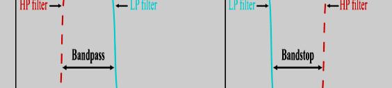
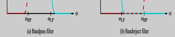
2 Common Filter Traner Function v. Freq H ( ) H( ) Low Pa High Pa Frequency H ( ) H ( ) Frequency Band dpa Band deject Frequency Frequency Slide
3 Filter Paive: reonant circuit that contain only paive element, namely reitor (), capacitor (C), and inductor (L) Active: reonant circuit that contain op amp, tranitor, and/or other active device, in addition to the paive element Slide 3
4 Filter Order The order o a ilter i equal to the abolute value o the highet power o ω in it traner unction Slide 4
5 Firt-Order Filter Circuit High Pa Low Pa V S + C Low Pa V S + L High Pa H / ( + 1/jωC) H C (1/jωC) / ( + 1/jωC) H / ( + jωl) H L jωl / ( + jωl) Slide 5

6 Firt Order Low Pa Filter Slide 6
7 Second-Order LC Filter Circuit Band Pa Z + 1/jωC + jωl V S + Low Pa High Pa C L Band eject H BP / Z H LP (1/jωC) j / Z H HP jωl / Z H B H LP + H HP Slide 7
8 Second Order BandPa Filter Write the expreion or V : Now ind H BP (ω): H BP V ( ω) V V S jωc ( 1 ω ω LC ) + j ω C Slide 8
9 Paive Filter: Bandpa Linear-Linear plot H BP V ( ω ) V S jωc ( 1 ω LC ) + jωc Slide 9
10 eonance Frequency Deined a requency when the total impedance i purely reitive ( i.e. zero imaginary i component) j Z( ω) + jωl ωcc Thereore Slide 1
")


11 db The Quality Factor Q The Quality Factor (Q) characterize the degree o electivity o the circuit. It i determined by: For a bandpa ilter: Notice that Q depend on the reonant requency Linear ω cale Slide 11
12 eonance Bandwidth / o 1/ At reonance with large Q, * Thi i a Linear-Linear plot V L and V C >>V L C Slide 1
13 Another Way to write H() (See Hambley text ) H H c c Hc 1 ( ) 1 1 L + jωl 1 jω jωc + + jωc + 1 ( ) ω ω 1 ωol 1 + jq ( ) QS ω ω ωoc 1 ( ) 1 ω o 1 + Q ( ) LC Slide 13
14 To Generate the Bode Plot 1 1 Low : dominate Hc( ) ; Hc( ) jq Q y 1log Hc ( ) K + log Slope : db / dec H ( ) 9 c High : dominate Hc( ), H ( ) y 1log H ( ) K log Slope : db / dec HH ( c ) 9 1 c jq Q c at : ( ) 1, ( ) 1 H H y db c c H ( ) c Slide 14

15 Bode Plot +db/dec -db/dec Slide 15
16 Second Order LowPa Filter V C 1 HLP ( ω ) V M LP ( ω) S ( 1 ω LC ) 1 + jωc { [ ( ) ] ( ) } 1 ω / ω + ω / ω 1/ 1 LC Q 1 ω L ω o Q ω o C o Slide 16
17 Another Way to write H() (See Hambley) H c 1 1 jωc jωc ( ) 1 1 L + + jωl 1+ + jω jω C jω C 1 1 ω L 1 Let ω, Hence ω L ; deine Q LC C ω C ω L jω ω L jω 1 ω 1 jω jω Q, Q ω ω jωc jω ω C ω H H c ω jq ( ) ω ω ω 1 + jq ( ) ω ω c ( ) Q 1 + Q ( ) Slide 17

 ( ω) V V L")
 (")
 ] + (")

18 Second Order HighPa Filter H M HP HP ( ω) ( ω) V V L S ω LC + jωc ( 1 ω LC ) ( ω / ω ) [ 1 ( ω / ω ) ] + ( ω / Qω ) { } 1/ Q Slide 18
19 Second Order Bandreject Filter H B VL + VC ( ω ) 1 H BP ( ω ) V S Slide 19
 1 Z p 1 1 + + jωc j ω L IZ p 1 1")

 1 1 + Qp ( ) I in L C p")
20 Parallel LC Circuit (See Hambley 6.7) 1 Z p jωc j ω L IZ p 1 1 H( ) I jωc 1+ + jωc jωl j ω L jω jω ω jω Qp, jωc j ωc Q jωl ω ωl ω ω ω 1 Hc( ) Q C 1 + jqp ( ) p ω ωl H c ( ) Qp ( ) I in L C p Slide
21 Active Filter Contain le component (no inductor) Traner unction that i inenitive to component tolerance or load variation Eaily adjuted d Allow a wide range o ueul traner unction Slide 1

 G")

22 Single Pole Lowpa Filter H LP Vout ( ω ) V 1 jωc jω C H LP ( ω ) G LP jω / ω LP G LP ; ωlp 1 C Slide
23 Single Pole Highpa Filter H HP H ( ω ) HP G ( ω) HP V V out jω / ω 1 + jω / ω HP HP Z Z j/ ω C G HP ; ωhp 1 C Slide 3
24 Cacaded Active Filter Slide 4


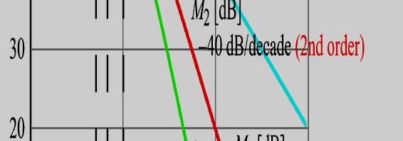
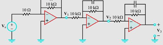
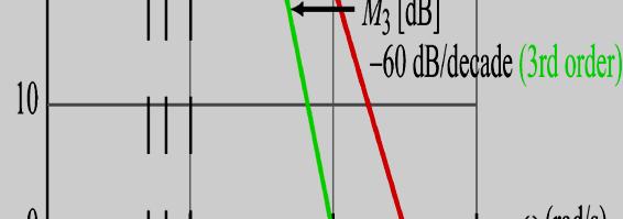
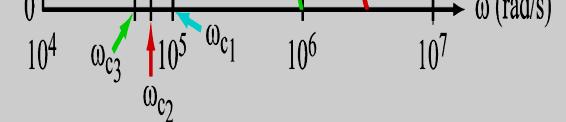
25 Cacaded Active Filter Slide 5


26 Cacaded Active Filter Slide 6


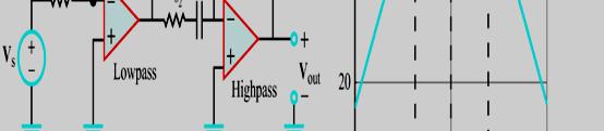
27 Cacaded Active Filter Slide 7
28 Cacaded Active Filter Slide 8
29 Cacaded Active Filter Slide 9
 See")


30 Appendix (For reerence only) See Hambley 14.5 The open loop gain o an Op Amp decreae with requency The unity-gain bandwidth t ~ everal MHz or typical op amp Slide 3
")

 Given: t")

31 Appendix (For reerence only) Circuit uppoed to have a cloed lop gain o 1 (db) Given: t 4MHz, circuit can operate with < 4kHz Slide 31
( ) 2. 1) Bode plots/transfer functions. a. Draw magnitude and phase bode plots for the transfer function
 2. 1) Bode plots/transfer functions. a. Draw magnitude and phase bode plots for the transfer function") ECSE CP7 olution Spring 5 ) Bode plot/tranfer function a. Draw magnitude and phae bode plot for the tranfer function H( ). ( ) ( E4) In your magnitude plot, indicate correction at the pole and zero. Step
ECSE CP7 olution Spring 5 ) Bode plot/tranfer function a. Draw magnitude and phae bode plot for the tranfer function H( ). ( ) ( E4) In your magnitude plot, indicate correction at the pole and zero. Step
Active Filters an Introduction
 Active Filter an Introduction + Vin() - Filter circuit G() + Vout() - Active Filter. Continuou-time or Sampled-data. Employ active element (e.g. tranitor, amplifier, op-amp) a. inductor-le (continuou-time)
SIMON FRASER UNIVERSITY School of Engineering Science ENSC 320 Electric Circuits II. Solutions to Assignment 3 February 2005.
 SIMON FRASER UNIVERSITY School of Engineering Science ENSC 320 Electric Circuit II Solution to Aignment 3 February 2005. Initial Condition Source 0 V battery witch flip at t 0 find i 3 (t) Component value:
EE221 Circuits II. Chapter 14 Frequency Response
 EE22 Circuits II Chapter 4 Frequency Response Frequency Response Chapter 4 4. Introduction 4.2 Transfer Function 4.3 Bode Plots 4.4 Series Resonance 4.5 Parallel Resonance 4.6 Passive Filters 4.7 Active
EE221 Circuits II. Chapter 14 Frequency Response
 EE22 Circuits II Chapter 4 Frequency Response Frequency Response Chapter 4 4. Introduction 4.2 Transfer Function 4.3 Bode Plots 4.4 Series Resonance 4.5 Parallel Resonance 4.6 Passive Filters 4.7 Active
Active Filters an Introduction
 Active Filter an Introduction + Vin() - Filter circuit G() + Vout() - Active Filter. Continuou-time or Sampled-data. Employ active element (e.g. tranitor, amplifier, op-amp) a. inductor-le (continuou-time)
Second-order filters. EE 230 second-order filters 1
 Second-order filters Second order filters: Have second order polynomials in the denominator of the transfer function, and can have zeroth-, first-, or second-order polynomials in the numerator. Use two
Designing Information Devices and Systems II Fall 2018 Elad Alon and Miki Lustig Discussion 5A
 EECS 6B Designing Information Devices and Systems II Fall 208 Elad Alon and Miki Lustig Discussion 5A Transfer Function When we write the transfer function of an arbitrary circuit, it always takes the
Solution: K m = R 1 = 10. From the original circuit, Z L1 = jωl 1 = j10 Ω. For the scaled circuit, L 1 = jk m ωl 1 = j10 10 = j100 Ω, Z L
 Problem 9.9 Circuit (b) in Fig. P9.9 is a scaled version of circuit (a). The scaling process may have involved magnitude or frequency scaling, or both simultaneously. If R = kω gets scaled to R = kω, supply
EE40 Midterm Review Prof. Nathan Cheung
 EE40 Midterm Review Prof. Nathan Cheung 10/29/2009 Slide 1 I feel I know the topics but I cannot solve the problems Now what? Slide 2 R L C Properties Slide 3 Ideal Voltage Source *Current depends d on
EE 508 Lecture 16. Filter Transformations. Lowpass to Bandpass Lowpass to Highpass Lowpass to Band-reject
 EE 508 Lecture 6 Filter Tranformation Lowpa to Bandpa Lowpa to Highpa Lowpa to Band-reject Review from Lat Time Theorem: If the perimeter variation and contact reitance are neglected, the tandard deviation
SIMON FRASER UNIVERSITY School of Engineering Science ENSC 320 Electric Circuits II. R 4 := 100 kohm
 SIMON FRASER UNIVERSITY School of Engineering Science ENSC 320 Electric Circuit II Solution to Aignment 3 February 2003. Cacaded Op Amp [DC&L, problem 4.29] An ideal op amp ha an output impedance of zero,
The general form for the transform function of a second order filter is that of a biquadratic (or biquad to the cool kids).
.") nd-order filters The general form for the transform function of a second order filter is that of a biquadratic (or biquad to the cool kids). T (s) A p s a s a 0 s b s b 0 As before, the poles of the transfer
nd-order filters The general form for the transform function of a second order filter is that of a biquadratic (or biquad to the cool kids). T (s) A p s a s a 0 s b s b 0 As before, the poles of the transfer
2nd-order filters. EE 230 second-order filters 1
 nd-order filters Second order filters: Have second order polynomials in the denominator of the transfer function, and can have zeroth-, first-, or second-order polyinomials in the numerator. Use two reactive
R-L-C Circuits and Resonant Circuits
 P517/617 Lec4, P1 R-L-C Circuits and Resonant Circuits Consider the following RLC series circuit What's R? Simplest way to solve for is to use voltage divider equation in complex notation. X L X C in 0
ECE Linear Circuit Analysis II
 ECE 202 - Linear Circuit Analyi II Final Exam Solution December 9, 2008 Solution Breaking F into partial fraction, F 2 9 9 + + 35 9 ft δt + [ + 35e 9t ]ut A 9 Hence 3 i the correct anwer. Solution 2 ft
EE 508 Lecture 16. Filter Transformations. Lowpass to Bandpass Lowpass to Highpass Lowpass to Band-reject
 EE 508 Lecture 6 Filter Tranformation Lowpa to Bandpa Lowpa to Highpa Lowpa to Band-reject Review from Lat Time Theorem: If the perimeter variation and contact reitance are neglected, the tandard deviation
CHAPTER 13 FILTERS AND TUNED AMPLIFIERS
 HAPTE FILTES AND TUNED AMPLIFIES hapter Outline. Filter Traniion, Type and Specification. The Filter Tranfer Function. Butterworth and hebyhev Filter. Firt Order and Second Order Filter Function.5 The
Sophomore Physics Laboratory (PH005/105)
") CALIFORNIA INSTITUTE OF TECHNOLOGY PHYSICS MATHEMATICS AND ASTRONOMY DIVISION Sophomore Physics Laboratory (PH5/15) Analog Electronics Active Filters Copyright c Virgínio de Oliveira Sannibale, 23 (Revision
CALIFORNIA INSTITUTE OF TECHNOLOGY PHYSICS MATHEMATICS AND ASTRONOMY DIVISION Sophomore Physics Laboratory (PH5/15) Analog Electronics Active Filters Copyright c Virgínio de Oliveira Sannibale, 23 (Revision
Poles, Zeros, and Frequency Response
 Complex Poles Poles, Zeros, and Frequency esponse With only resistors and capacitors, you're stuck with real poles. If you want complex poles, you need either an op-amp or an inductor as well. Complex
Chapter 9: Controller design. Controller design. Controller design
 Chapter 9. Controller Deign 9.. Introduction 9.2. Eect o negative eedback on the network traner unction 9.2.. Feedback reduce the traner unction rom diturbance to the output 9.2.2. Feedback caue the traner
Question 1 Equivalent Circuits
 MAE 40 inear ircuit Fall 2007 Final Intruction ) Thi exam i open book You may ue whatever written material you chooe, including your cla note and textbook You may ue a hand calculator with no communication
CHAPTER 14 SIGNAL GENERATORS AND WAVEFORM-SHAPING CIRCUITS
 CHAPTE 4 SIGNA GENEATS AN WAEFM-SHAPING CICUITS Chapter utline 4. Baic Principle o Sinuoidal cillator 4. p Amp-C cillator 4. C and Crytal cillator 4.4 Bitable Multiibrator 4.5 Generation o Square and Triangular
DC and AC Impedance of Reactive Elements
 3/6/20 D and A Impedance of Reactive Elements /6 D and A Impedance of Reactive Elements Now, recall from EES 2 the complex impedances of our basic circuit elements: ZR = R Z = jω ZL = jωl For a D signal
EE 40: Introduction to Microelectronic Circuits Spring 2008: Midterm 2
 EE 4: Introduction to Microelectronic Circuits Spring 8: Midterm Venkat Anantharam 3/9/8 Total Time Allotted : min Total Points:. This is a closed book exam. However, you are allowed to bring two pages
ECEN620: Network Theory Broadband Circuit Design Fall 2018
 ECEN60: Network Theory Broadband Circuit Deign Fall 08 Lecture 6: Loop Filter Circuit Sam Palermo Analog & Mixed-Signal Center Texa A&M Univerity Announcement HW i due Oct Require tranitor-level deign
s 0.068μ s Rearrange the function into a more convenient form and verify that it is still equal to the original.
 Title: TCS Traner Function Author: Eric Warmbier Decription: Thi document derive the variou traner unction or the TCS ytem on the IRTF. The ytem i broken down into block in a Viio document. A traner unction
09/29/2009 Reading: Hambley Chapter 5 and Appendix A
 EE40 Lec 10 Complex Numbers and Phasors Prof. Nathan Cheung 09/29/2009 Reading: Hambley Chapter 5 and Appendix A Slide 1 OUTLINE Phasors as notation for Sinusoids Arithmetic with Complex Numbers Complex
Lecture 28. Passive HP Filter Design
 Lecture 28. Paive HP Filter Deign STRATEGY: Convert HP pec to Equivalent NLP pec. Deign an appropriate 3dB NLP tranfer function. Realize the 3dB NLP tranfer function a a circuit. Convert the 3dB NLP circuit
Dynamic circuits: Frequency domain analysis
 Electronic Circuits 1 Dynamic circuits: Contents Free oscillation and natural frequency Transfer functions Frequency response Bode plots 1 System behaviour: overview 2 System behaviour : review solution
AC analysis - many examples
 AC analysis - many examples The basic method for AC analysis:. epresent the AC sources as complex numbers: ( ). Convert resistors, capacitors, and inductors into their respective impedances: resistor Z
Phasors: Impedance and Circuit Anlysis. Phasors
 Phasors: Impedance and Circuit Anlysis Lecture 6, 0/07/05 OUTLINE Phasor ReCap Capacitor/Inductor Example Arithmetic with Complex Numbers Complex Impedance Circuit Analysis with Complex Impedance Phasor
Prof. D. Manstretta LEZIONI DI FILTRI ANALOGICI. Danilo Manstretta AA
 AA-3 LEZIONI DI FILTI ANALOGICI Danilo Manstretta AA -3 AA-3 High Order OA-C Filters H() s a s... a s a s a n s b s b s b s b n n n n... The goal of this lecture is to learn how to design high order OA-C
OPERATIONAL AMPLIFIER APPLICATIONS
 OPERATIONAL AMPLIFIER APPLICATIONS 2.1 The Ideal Op Amp (Chapter 2.1) Amplifier Applications 2.2 The Inverting Configuration (Chapter 2.2) 2.3 The Non-inverting Configuration (Chapter 2.3) 2.4 Difference
Lecture 4: R-L-C Circuits and Resonant Circuits
 Lecture 4: R-L-C Circuits and Resonant Circuits RLC series circuit: What's V R? Simplest way to solve for V is to use voltage divider equation in complex notation: V X L X C V R = in R R + X C + X L L
I. Frequency Response of Voltage Amplifiers
 I. Frequency Response of Voltage Amplifiers A. Common-Emitter Amplifier: V i SUP i OUT R S V BIAS R L v OUT V Operating Point analysis: 0, R s 0, r o --->, r oc --->, R L ---> Find V BIAS such that I C
( s) N( s) ( ) The transfer function will take the form. = s = 2. giving ωo = sqrt(1/lc) = 1E7 [rad/s] ω 01 := R 1. α 1 2 L 1.
![( s) N( s) ( ) The transfer function will take the form. = s = 2. giving ωo = sqrt(1/lc) = 1E7 [rad/s] ω 01 := R 1. α 1 2 L 1.](/thumbs/83/87520964.jpg "( s) N( s) ( ) The transfer function will take the form. = s = 2. giving ωo = sqrt(1/lc) = 1E7 [rad/s] ω 01 := R 1. α 1 2 L 1.") Problem ) RLC Parallel Circuit R L C E-4 E-0 V a. What is the resonant frequency of the circuit? The transfer function will take the form N ( ) ( s) N( s) H s R s + α s + ω s + s + o L LC giving ωo sqrt(/lc)
Problem ) RLC Parallel Circuit R L C E-4 E-0 V a. What is the resonant frequency of the circuit? The transfer function will take the form N ( ) ( s) N( s) H s R s + α s + ω s + s + o L LC giving ωo sqrt(/lc)
Sinusoidal Steady-State Analysis
 Chapter 4 Sinusoidal Steady-State Analysis In this unit, we consider circuits in which the sources are sinusoidal in nature. The review section of this unit covers most of section 9.1 9.9 of the text.
ECE3050 Assignment 7
 ECE3050 Assignment 7. Sketch and label the Bode magnitude and phase plots for the transfer functions given. Use loglog scales for the magnitude plots and linear-log scales for the phase plots. On the magnitude
Midterm 1 Announcements
 Midterm Announcements eiew session: 5-8pm TONIGHT 77 Cory Midterm : :30-pm on Tuesday, July Dwelle 45. Material coered HW-3 Attend only your second lab slot this wee EE40 Summer 005: Lecture 9 Instructor:
Chapter 6 Frequency Response, Bode Plots and Resonance
 Chapter 6 Frequency Response, Bode Plots and Resonance Signal Processg is concerned with manipulatg Signals to extract Inormation and to use that ormation to generate other useul Signals Goal. Fundamental
55:041 Electronic Circuits
 55:04 Electronic ircuit Frequency eone hater 7 A. Kruger Frequency eone- ee age 4-5 o the Prologue in the text Imortant eview v = M co ωt + θ m = M e e j ωt+θ m = e M e jθ me jωt Thi lead to the concet
Lecture 6: Resonance II. Announcements
 EES 5 Spring 4, Lecture 6 Lecture 6: Reonance II EES 5 Spring 4, Lecture 6 Announcement The lab tart thi week You mut how up for lab to tay enrolled in the coure. The firt lab i available on the web ite,
Electronic Circuits EE359A
 Electronic Circuits EE359A Bruce McNair B26 bmcnair@stevens.edu 21-216-5549 Lecture 22 578 Second order LCR resonator-poles V o I 1 1 = = Y 1 1 + sc + sl R s = C 2 s 1 s + + CR LC s = C 2 sω 2 s + + ω
Bandwidth of op amps. R 1 R 2 1 k! 250 k!
 Bandwidth of op amps An experiment - connect a simple non-inverting op amp and measure the frequency response. From the ideal op amp model, we expect the amp to work at any frequency. Is that what happens?
ECE-202 FINAL December 13, 2016 CIRCLE YOUR DIVISION
 ECE-202 Final, Fall 16 1 ECE-202 FINAL December 13, 2016 Name: (Pleae print clearly.) Student Email: CIRCLE YOUR DIVISION DeCarlo- 8:30-9:30 Talavage-9:30-10:30 2021 2022 INSTRUCTIONS There are 35 multiple
ECEN 325 Electronics
 ECEN 325 Electronics Operational Amplifiers Dr. Aydın İlker Karşılayan Texas A&M University Department of Electrical and Computer Engineering Opamp Terminals positive supply inverting input terminal non
EE 508 Lecture 6. Scaling, Normalization and Transformation
 EE 508 Lecture 6 Scalig, Normalizatio ad Traformatio Review from Lat Time Dead Network X IN T X OUT T X OUT N T = D D The dead etwork of ay liear circuit i obtaied by ettig ALL idepedet ource to zero.
Homework Assignment No. 3 - Solutions
 ECE 6440 Summer 2003 Page 1 Homework Aignment o. 3 Problem 1 (10 point) Aume an LPLL ha F() 1 and the PLL parameter are 0.8V/radian, K o 100 MHz/V, and the ocillation frequency, f oc 500MHz. Sketch the
EE 508 Lecture 16. Filter Transformations. Lowpass to Bandpass Lowpass to Highpass Lowpass to Band-reject
 EE 508 Lecture 6 Filter Tranformation Lowpa to Bandpa Lowpa to Highpa Lowpa to Band-reject Review from Lat Time Flat Paband/Stopband Filter T j T j Lowpa Bandpa T j T j Highpa Bandreject Review from Lat
Design of Narrow Band Filters Part 1
 E.U.I.T. Telecomunicación 2010, Madrid, Spain, 27.09 30.09.2010 Design of Narrow Band Filters Part 1 Thomas Buch Institute of Communications Engineering University of Rostock Th. Buch, Institute of Communications
6.17 The Lossy Voice-Coil Inductance
 6.7. THE LOSSY VOICE-COIL INDUCTANCE Solution. The impedance function is given by (/3.3) (s/38.2) Z VC (s) =7+0.008s +70 (s/38.2) 2 +(/3.3) (s/38.2) + Example 0 Solve for the element values in the equivalent
Lecture 16 FREQUENCY RESPONSE OF SIMPLE CIRCUITS
 Lecture 6 FREQUENCY RESPONSE OF SIMPLE CIRCUITS Ray DeCarlo School of ECE Purdue University West Lafayette, IN 47907-285 decarlo@ecn.purdue.edu EE-202, Frequency Response p 2 R. A. DeCarlo I. WHAT IS FREQUENCY
Asymptote. 2 Problems 2 Methods
 Asymptote Problems Methods Problems Assume we have the ollowing transer unction which has a zero at =, a pole at = and a pole at =. We are going to look at two problems: problem is where >> and problem
Sinusoidal Steady State Analysis (AC Analysis) Part I
 Part I") Sinusoidal Steady State Analysis (AC Analysis) Part I Amin Electronics and Electrical Communications Engineering Department (EECE) Cairo University elc.n102.eng@gmail.com http://scholar.cu.edu.eg/refky/
Sinusoidal Steady State Analysis (AC Analysis) Part I Amin Electronics and Electrical Communications Engineering Department (EECE) Cairo University elc.n102.eng@gmail.com http://scholar.cu.edu.eg/refky/
Steady State Frequency Response Using Bode Plots
 School of Engineering Department of Electrical and Computer Engineering 332:224 Principles of Electrical Engineering II Laboratory Experiment 3 Steady State Frequency Response Using Bode Plots 1 Introduction
Name: (Please print clearly) Student ID: CIRCLE YOUR DIVISION INSTRUCTIONS
 Student ID: CIRCLE YOUR DIVISION INSTRUCTIONS") EE 202 Exam III April 13 2011 Name: (Please print clearly) Student ID: CIRCLE YOUR DIVISION Morning 7:30 MWF Furgason INSTRUCTIONS Afternoon 3:30 MWF DeCarlo There are 10 multiple choice worth 5 points
EE 202 Exam III April 13 2011 Name: (Please print clearly) Student ID: CIRCLE YOUR DIVISION Morning 7:30 MWF Furgason INSTRUCTIONS Afternoon 3:30 MWF DeCarlo There are 10 multiple choice worth 5 points
Homework Assignment 11
 Homework Assignment Question State and then explain in 2 3 sentences, the advantage of switched capacitor filters compared to continuous-time active filters. (3 points) Continuous time filters use resistors
Chapter 8: Converter Transfer Functions
 Chapter 8. Converter Transfer Functions 8.1. Review of Bode plots 8.1.1. Single pole response 8.1.2. Single zero response 8.1.3. Right half-plane zero 8.1.4. Frequency inversion 8.1.5. Combinations 8.1.6.
ESE319 Introduction to Microelectronics. Feedback Basics
 Feedback Basics Feedback concept Feedback in emitter follower Stability One-pole feedback and root locus Frequency dependent feedback and root locus Gain and phase margins Conditions for closed loop stability
6.1 Introduction
 6. Introduction A.C Circuits made up of resistors, inductors and capacitors are said to be resonant circuits when the current drawn from the supply is in phase with the impressed sinusoidal voltage. Then.
EE/ME/AE324: Dynamical Systems. Chapter 8: Transfer Function Analysis
 EE/ME/AE34: Dynamical Sytem Chapter 8: Tranfer Function Analyi The Sytem Tranfer Function Conider the ytem decribed by the nth-order I/O eqn.: ( n) ( n 1) ( m) y + a y + + a y = b u + + bu n 1 0 m 0 Taking
EE105 Fall 2015 Microelectronic Devices and Circuits Frequency Response. Prof. Ming C. Wu 511 Sutardja Dai Hall (SDH)
") EE05 Fall 205 Microelectronic Devices and Circuits Frequency Response Prof. Ming C. Wu wu@eecs.berkeley.edu 5 Sutardja Dai Hall (SDH) Amplifier Frequency Response: Lower and Upper Cutoff Frequency Midband
EE05 Fall 205 Microelectronic Devices and Circuits Frequency Response Prof. Ming C. Wu wu@eecs.berkeley.edu 5 Sutardja Dai Hall (SDH) Amplifier Frequency Response: Lower and Upper Cutoff Frequency Midband
EE-202 Exam III April 6, 2017
 EE-202 Exam III April 6, 207 Name: (Please print clearly.) Student ID: CIRCLE YOUR DIVISION DeCarlo--202 DeCarlo--2022 7:30 MWF :30 T-TH INSTRUCTIONS There are 3 multiple choice worth 5 points each and
Use of a Notch Filter in a Tuned Mode for LISA.
 Use of a Notch Filter in a Tuned Mode for LISA. Giorgio Fontana September 00 Abstract. During interferometric measurements the proof mass must be free from any controlling force within a given observation
Chapter 2 Circuit Elements
 Chapter Circuit Elements Chapter Circuit Elements.... Introduction.... Circuit Element Construction....3 Resistor....4 Inductor...4.5 Capacitor...6.6 Element Basics...8.6. Element Reciprocals...8.6. Reactance...8.6.3
Design of Digital Filters
 Deign of Digital Filter Paley-Wiener Theorem [ ] ( ) If h n i a caual energy ignal, then ln H e dω< B where B i a finite upper bound. One implication of the Paley-Wiener theorem i that a tranfer function
Switched Capacitor: Sampled Data Systems
 Switched Capacitor: Sampled Data Systems Basic switched capacitor theory How has Anadigm utilised this. Theory-Basic SC and Anadigm-1 Resistor & Charge Relationship I + V - I Resistance is defined in terms
Stability of Operational amplifiers
 Stability o Operational ampliiers Willy Sansen KULeuven, ESAT-MICAS Leuven, Belgium willy.sansen@esat.kuleuven.be Willy Sansen 0-05 05 Table o contents Use o operational ampliiers Stability o 2-stage opamp
Electronic Circuits Summary
 Electronic Circuits Summary Andreas Biri, D-ITET 6.06.4 Constants (@300K) ε 0 = 8.854 0 F m m 0 = 9. 0 3 kg k =.38 0 3 J K = 8.67 0 5 ev/k kt q = 0.059 V, q kt = 38.6, kt = 5.9 mev V Small Signal Equivalent
Frequency Response. Re ve jφ e jωt ( ) where v is the amplitude and φ is the phase of the sinusoidal signal v(t). ve jφ
 where v is the amplitude and φ is the phase of the sinusoidal signal v(t). ve jφ") 27 Frequency Response Before starting, review phasor analysis, Bode plots... Key concept: small-signal models for amplifiers are linear and therefore, cosines and sines are solutions of the linear differential
27 Frequency Response Before starting, review phasor analysis, Bode plots... Key concept: small-signal models for amplifiers are linear and therefore, cosines and sines are solutions of the linear differential
R. W. Erickson. Department of Electrical, Computer, and Energy Engineering University of Colorado, Boulder
 R. W. Erickson Department of Electrical, Computer, and Energy Engineering University of Colorado, Boulder 8.1. Review of Bode plots Decibels Table 8.1. Expressing magnitudes in decibels G db = 0 log 10
5.5 Application of Frequency Response: Signal Filters
 44 Dynamic Sytem Second order lowpa filter having tranfer function H()=H ()H () u H () H () y Firt order lowpa filter Figure 5.5: Contruction of a econd order low-pa filter by combining two firt order
Active Filter Design by Carsten Kristiansen Napier University. November 2004
 by Carsten Kristiansen November 2004 Title page Author: Carsten Kristiansen. Napier No: 0400772. Assignment partner: Benjamin Grydehoej. Assignment title:. Education: Electronic and Computer Engineering.
55:041 Electronic Circuits
 55:04 Electronic ircuit Frequency epone hapter 7 A. Kruger Frequency epone- ee page 4-5 of the Prologue in the text Important eview co Thi lead to the concept of phaor we encountered in ircuit In Linear
ECE Spring 2015 Final Exam
 ECE 20100 Spring 2015 Final Exam May 7, 2015 Section (circle below) Jung (1:30) 0001 Qi (12:30) 0002 Peleato (9:30) 0004 Allen (10:30) 0005 Zhu (4:30) 0006 Name PUID Instructions 1. DO NOT START UNTIL
Chapter 8: Converter Transfer Functions
 Chapter 8. Converter Transer Functions 8.1. Review o Bode plots 8.1.1. Single pole response 8.1.2. Single zero response 8.1.3. Right hal-plane zero 8.1.4. Frequency inversion 8.1.5. Combinations 8.1.6.
Homework 6 Solutions and Rubric
 Homework 6 Solutions and Rubric EE 140/40A 1. K-W Tube Amplifier b) Load Resistor e) Common-cathode a) Input Diff Pair f) Cathode-Follower h) Positive Feedback c) Tail Resistor g) Cc d) Av,cm = 1/ Figure
Today. 1/25/11 Physics 262 Lecture 2 Filters. Active Components and Filters. Homework. Lab 2 this week
 /5/ Physics 6 Lecture Filters Today Basics: Analog versus Digital; Passive versus Active Basic concepts and types of filters Passband, Stopband, Cut-off, Slope, Knee, Decibels, and Bode plots Active Components
Reference:W:\Lib\MathCAD\Default\defaults.mcd
 4/9/9 Page of 5 Reference:W:\Lib\MathCAD\Default\default.mcd. Objective a. Motivation. Finite circuit peed, e.g. amplifier - effect on ignal. E.g. how "fat" an amp do we need for audio? For video? For
EE 508 Lecture 6. Dead Networks Scaling, Normalization and Transformations
 EE 508 Lecture 6 Dead Network Scalig, Normalizatio ad Traformatio Filter Cocept ad Termiology 2-d order polyomial characterizatio Biquadratic Factorizatio Op Amp Modelig Stability ad Itability Roll-off
Sinusoidal Steady-state Analysis
 Siusoidal Steady-state Aalysis Complex umber reviews Phasors ad ordiary differetial equatios Complete respose ad siusoidal steady-state respose Cocepts of impedace ad admittace Siusoidal steady-state aalysis
EE100Su08 Lecture #11 (July 21 st 2008)
") EE100Su08 Lecture #11 (July 21 st 2008) Bureaucratic Stuff Lecture videos should be up by tonight HW #2: Pick up from office hours today, will leave them in lab. REGRADE DEADLINE: Monday, July 28 th 2008,
EE100Su08 Lecture #11 (July 21 st 2008) Bureaucratic Stuff Lecture videos should be up by tonight HW #2: Pick up from office hours today, will leave them in lab. REGRADE DEADLINE: Monday, July 28 th 2008,
MAE140 Linear Circuits Fall 2012 Final, December 13th
 MAE40 Linear Circuit Fall 202 Final, December 3th Intruction. Thi exam i open book. You may ue whatever written material you chooe, including your cla note and textbook. You may ue a hand calculator with
Frequency Dependent Aspects of Op-amps
 Frequency Dependent Aspects of Op-amps Frequency dependent feedback circuits The arguments that lead to expressions describing the circuit gain of inverting and non-inverting amplifier circuits with resistive
Feedback design for the Buck Converter
 Feedback design for the Buck Converter Portland State University Department of Electrical and Computer Engineering Portland, Oregon, USA December 30, 2009 Abstract In this paper we explore two compensation
DESIGN MICROELECTRONICS ELCT 703 (W17) LECTURE 3: OP-AMP CMOS CIRCUIT. Dr. Eman Azab Assistant Professor Office: C
 LECTURE 3: OP-AMP CMOS CIRCUIT. Dr. Eman Azab Assistant Professor Office: C") MICROELECTRONICS ELCT 703 (W17) LECTURE 3: OP-AMP CMOS CIRCUIT DESIGN Dr. Eman Azab Assistant Professor Office: C3.315 E-mail: eman.azab@guc.edu.eg 1 TWO STAGE CMOS OP-AMP It consists of two stages: First
MICROELECTRONICS ELCT 703 (W17) LECTURE 3: OP-AMP CMOS CIRCUIT DESIGN Dr. Eman Azab Assistant Professor Office: C3.315 E-mail: eman.azab@guc.edu.eg 1 TWO STAGE CMOS OP-AMP It consists of two stages: First
UNIVERSITY OF CALIFORNIA College of Engineering Department of Electrical Engineering and Computer Sciences
 UNIVERSITY OF CALIFORNIA College of Engineering Department of Electrical Engineering and Computer Sciences E. Alon Final EECS 240 Monday, May 19, 2008 SPRING 2008 You should write your results on the exam
Stability and Frequency Compensation
 類比電路設計 (3349) - 2004 Stability and Frequency ompensation hing-yuan Yang National hung-hsing University Department of Electrical Engineering Overview Reading B Razavi hapter 0 Introduction In this lecture,
Introduction to Laplace Transform Techniques in Circuit Analysis
 Unit 6 Introduction to Laplace Tranform Technique in Circuit Analyi In thi unit we conider the application of Laplace Tranform to circuit analyi. A relevant dicuion of the one-ided Laplace tranform i found
Biquad Filter. by Kenneth A. Kuhn March 8, 2013
 by Kenneth A. Kuhn March 8, 201 The biquad filter implements both a numerator and denominator quadratic function in s thus its name. All filter outputs have identical second order denominator in s and
EE105 - Fall 2005 Microelectronic Devices and Circuits
 EE5 - Fall 5 Microelectronic Device and ircuit Lecture 9 Second-Order ircuit Amplifier Frequency Repone Announcement Homework 8 due tomorrow noon Lab 7 next week Reading: hapter.,.3. Lecture Material Lat
EE247 Lecture 10. Switched-Capacitor Integrator C
 EE247 Lecture 0 Switched-apacitor Filter Switched-capacitor integrator DDI integrator LDI integrator Effect of paraitic capacitance Bottom-plate integrator topology Reonator Bandpa filter Lowpa filter
Consider a simple RC circuit. We might like to know how much power is being supplied by the source. We probably need to find the current.
 AC power Consider a simple RC circuit We might like to know how much power is being supplied by the source We probably need to find the current R 10! R 10! is VS Vmcosωt Vm 10 V f 60 Hz V m 10 V C 150
Keysight Technologies Heidi Barnes
 Keysight Technologies 2018.03.29 Heidi Barnes 1 S I G N A L I N T E G R I T Y A N D P O W E R I N T E G R I T Y Hewlett-Packard Agilent Technologies Keysight Technologies Bill and Dave s Company and the
K.K. Gan L3: R-L-C AC Circuits. amplitude. Volts. period. -Vo
 Lecture 3: R-L-C AC Circuits AC (Alternative Current): Most of the time, we are interested in the voltage at a point in the circuit will concentrate on voltages here rather than currents. We encounter
Digital Control System
 Digital Control Sytem - A D D A Micro ADC DAC Proceor Correction Element Proce Clock Meaurement A: Analog D: Digital Continuou Controller and Digital Control Rt - c Plant yt Continuou Controller Digital
Lowpass L Matching Network Designer
 Lowpass L Matching Network Designer V S L V L I S j*x S C j*x L Table of Contents I. General Impedance Matching II. Impedance Transformation for Power Amplifiers III. Inputs IV. Calculations V. Outputs
Electric Circuits I FINAL EXAMINATION
 EECS:300, Electric Circuits I s6fs_elci7.fm - Electric Circuits I FINAL EXAMINATION Problems Points.. 3. 0 Total 34 Was the exam fair? yes no 5//6 EECS:300, Electric Circuits I s6fs_elci7.fm - Problem
ECE137B Final Exam. Wednesday 6/8/2016, 7:30-10:30PM.
 ECE137B Final Exam Wednesday 6/8/2016, 7:30-10:30PM. There are7 problems on this exam and you have 3 hours There are pages 1-32 in the exam: please make sure all are there. Do not open this exam until