PN Junctions. Lecture 7
|
|
|
- Martina Cooper
- 5 years ago
- Views:
Transcription
1 Lecture 7 PN Junctions Kathy Aidala Applied Physics, G2 Harvard University 10 October, 2002 Wei 1
2 Active Circuit Elements Why are they desirable? Much greater flexibility in circuit applications. What s possible/impossible? Can you make it from a single device, or do you need to combine several into one unit? If you could have a device that does anything, what would it be? How are they made? - Exploit physical properties of the natural world - Enhance/alter what s available naturally Reading: Sedra & Smith 3.3, Streetman Ch 5 Wei 2
3 PN Junction Diode qv I = I e kt 1 0 Subtracting 1 becomes negligible for higher applied V. I>>I0 kt q 26mV at room temp Wei 3
4 Band Diagram qv 0qV0 P-type material is brought into contact with n-type material. The Fermi levels must be at equilibrium. Band Bending: The conduction and valence bands bend to bring the Fermi levels into contact. Wei 4
5 What happens when p-type meets n-type? Holes diffuse from the p-type into the n-type, electrons diffuse from the n-type into the p-type, creating a diffusion current. The diffusion equation is given by dn J n = qd n dx D n = diffusion constant Once the holes [electrons] cross into the n-type [p-type] region, they recombine with the electrons [holes]. This recombination strips the n-type [p-type] of its electrons near the boundary, creating an electric field due to excess charge. The region stripped of carriers is called the space-charge region, or depletion region. V 0 is the contact potential that exists due to the electric field. E(x) = dv dx Some carriers are generated and make their way into the depletion region where they are whisked away by the electric field, creating a drift current. Wei 5
6 Equilibrium motion of carriers dn(x) J n (x) = qµ n n(x)e(x) + qd n dx dp(x) J p (x) = qµ p p(x)e(x) + qd p dx Drift Diffusion At equilibrium, the two componentsare equal D µ = kt q The diffusion current is determined by the number of carriers able to overcome the potential. The drift current is determined by the generation of minority carriers which then feel the field and get whisked across. This generation rate is determined by the temperature. Einstein' s relation Wei 6

7 Space Charge at a junction 5-9 qx p0 AN a = qx n0 AN d x n0 = N a x p0 N d W dep = 2ε q N a N d V 0 Wei 7
8 Forward Bias + V - p n Forward bias: apply a positive voltage to the p-type, negative to n-type. Decrease the built-in potential, lower the barrier height. Increase the number of carriers able to diffuse across the barrier Diffusion current increases Drift current remains the same Current flows from p to n Wei 8
9 Reverse Bias - V + p n Reverse bias: apply a negative voltage to the p-type, positive to n-type. Increase the built-in potential, lower the barrier height. Decrease the number of carriers able to diffuse across the barrier. Diffusion current decreases. Drift current remains the same. Almost no current flows. Reverse leakage current, I 0, is the drift current, flowing from n to p. Wei 9
10 Review of Biasing Applying a bias adds or subtracts to the built-in potential. This changes the diffusion current, making it harder or easier for the carriers to diffuse across. The drift current is essentially constant, as it is dependent on temperature. Wei 10
11 Quantitative Analysis of Current Flow Consider the holes that can now diffuse across to the n-type region. p n (x n ) = p n 0 e qv kt p n (x) = [ p n0 + (p n (x n ) p n 0 ]e (x x n ) L p J p = q D p p n 0 e qv kt 1 L p L p = diffusion length e ( x x n ) LP But with the applied voltage, the electrons that get consumed by the holes are replenished from the circuit, at a constant rate determined by the vale at x n, simplifying this to Wei 11
12 Analysis Continued J p = q D p p n0 e qv kt 1 L p Smilarly, for the electrons in the p-type, one obtains J n = q D n n p0 e qv kt 1 L n A bit of manipulation gives us 2 D I = Aqn p i L p N d + D n L n N a 2 D I 0 = Aqn p i + D n L p N d L n N a kt eqv 1 Reverse saturation current, the drift current, depends directly on the area of the junction. Also depends on n i, which is dependent on temperature. Wei 12
13 Capacitance The junction acts as a parallel plate capacitor. Charge builds up on both sides. C j = ε A s W dep = W dep 2ε s q N a N d This expression is accurate for reverse bias, but not very good for forward bias. V+V 0 is the total voltage across the junction under reverse bias conditions. We can also write this as ( V + V 0 ) C j = C j 0 1+ V R V 0 Notice we can use a diode as a varactor! (Voltage controlled capacitor.) Wei 13
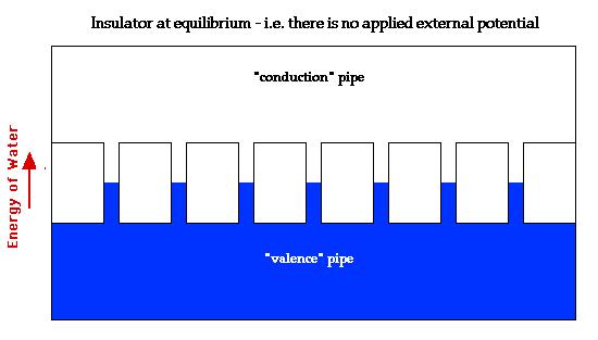
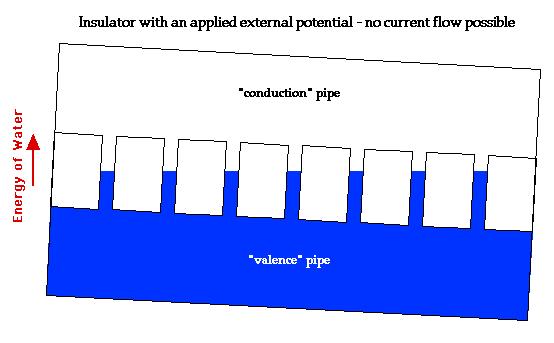
14 Two pipe/fluid model Wei 14

15 More fluid Models Wei 15

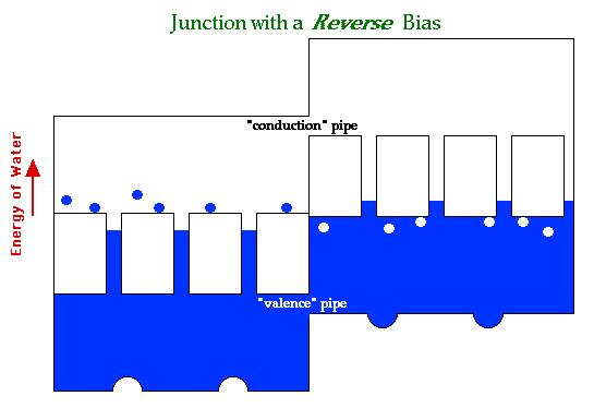
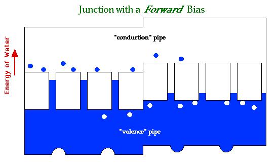
16 And more! Wei 16
17 Reverse Breakdown Zener Breakdown: The bands bend so much that carriers tunnel through the depletion region. This will occur in heavily doped junctions when the n-side conduction band appears opposite the p-side valence band. Avalanche Breakdown: carriers have enough energy to ionize an electron-hole-pair, creating more highly energetic carriers, which collide to form more EHPs, which creates Wei 17
18 Photodiodes Diodes have an optical generation rate. Carriers are created by shining light with intensity greater than the bandgap. One wants large depletion widths and long diffusion lengths, as it is only in these areas that excited carriers will make it across the junction. Photodetector: operate in third quadrant. Compromise between speed and junction width leads to a p-intrisic-n junction, where carriers will be rapidly swept across, and can quickly diffuse in the p and n regions. Solar Cell: operating in the fourth quadrant generates current, though small. Wei 18

19 Light Emitting Diodes When electrons and holes combine, they release energy. This energy is often released as heat into the lattice, but in some materials, known as direct bandgap materials, they release light. Engineering LEDs can be difficult, but has been done over a wide range of wavelengths. This illustration describes the importance of the plastic bubble in directing the light so that it is more effectively seen. Wei 19
ECE 340 Lecture 27 : Junction Capacitance Class Outline:
 ECE 340 Lecture 27 : Junction Capacitance Class Outline: Breakdown Review Junction Capacitance Things you should know when you leave M.J. Gilbert ECE 340 Lecture 27 10/24/11 Key Questions What types of
Semiconductor Physics and Devices
 The pn Junction 1) Charge carriers crossing the junction. 3) Barrier potential Semiconductor Physics and Devices Chapter 8. The pn Junction Diode 2) Formation of positive and negative ions. 4) Formation
EECS130 Integrated Circuit Devices
 EECS130 Integrated Circuit Devices Professor Ali Javey 9/18/2007 P Junctions Lecture 1 Reading: Chapter 5 Announcements For THIS WEEK OLY, Prof. Javey's office hours will be held on Tuesday, Sept 18 3:30-4:30
Current mechanisms Exam January 27, 2012
 Current mechanisms Exam January 27, 2012 There are four mechanisms that typically cause currents to flow: thermionic emission, diffusion, drift, and tunneling. Explain briefly which kind of current mechanisms
Diodes. anode. cathode. cut-off. Can be approximated by a piecewise-linear-like characteristic. Lecture 9-1
 Diodes mplest nonlinear circuit element Basic operation sets the foundation for Bipolar Junction Transistors (BJTs) Also present in Field Effect Transistors (FETs) Ideal diode characteristic anode cathode
p-n junction biasing, p-n I-V characteristics, p-n currents Norlaili Mohd. Noh EEE /09
 CLASS 6&7 p-n junction biasing, p-n I-V characteristics, p-n currents 1 p-n junction biasing Unbiased p-n junction: the potential barrier is 0.7 V for Si and 0.3 V for Ge. Nett current across the p-n junction
FYS3410 Condensed matter physics
 FYS3410 Condensed matter physics Lecture 23 and 24: pn-junctions and electrooptics Randi Haakenaasen UniK/UiO Forsvarets forskningsinstitutt 11.05.2016 and 18.05.2016 Outline Why pn-junctions are important
Consider a uniformly doped PN junction, in which one region of the semiconductor is uniformly doped with acceptor atoms and the adjacent region is
 CHAPTER 7 The PN Junction Consider a uniformly doped PN junction, in which one region of the semiconductor is uniformly doped with acceptor atoms and the adjacent region is uniformly doped with donor atoms.
Photosynthesis & Solar Power Harvesting
 Lecture 23 Semiconductor Detectors - Photodetectors Principle of the pn junction photodiode Absorption coefficient and photodiode materials Properties of semiconductor detectors The pin photodiodes Avalanche
n N D n p = n i p N A
 Summary of electron and hole concentration in semiconductors Intrinsic semiconductor: E G n kt i = pi = N e 2 0 Donor-doped semiconductor: n N D where N D is the concentration of donor impurity Acceptor-doped
The pn junction. [Fonstad, Ghione]
![The pn junction. [Fonstad, Ghione]](/thumbs/93/112370833.jpg "The pn junction. [Fonstad, Ghione]") The pn junction [Fonstad, Ghione] Band diagram On the vertical axis: potential energy of the electrons On the horizontal axis: now there is nothing: later we ll put the position qf s : work function (F
The pn junction [Fonstad, Ghione] Band diagram On the vertical axis: potential energy of the electrons On the horizontal axis: now there is nothing: later we ll put the position qf s : work function (F
Chapter 7. The pn Junction
 Chapter 7 The pn Junction Chapter 7 PN Junction PN junction can be fabricated by implanting or diffusing donors into a P-type substrate such that a layer of semiconductor is converted into N type. Converting
Peak Electric Field. Junction breakdown occurs when the peak electric field in the PN junction reaches a critical value. For the N + P junction,
 Peak Electric Field Junction breakdown occurs when the peak electric field in the P junction reaches a critical value. For the + P junction, qa E ( x) ( xp x), s W dep 2 s ( bi Vr ) 2 s potential barrier
ECE 340 Lecture 21 : P-N Junction II Class Outline:
 ECE 340 Lecture 21 : P-N Junction II Class Outline: Contact Potential Equilibrium Fermi Levels Things you should know when you leave Key Questions What is the contact potential? Where does the transition
Key Questions. ECE 340 Lecture 27 : Junction Capacitance 4/6/14. Class Outline: Breakdown Review Junction Capacitance
 ECE 340 Lecture 27 : Junction Capacitance Breakdown Reiew Class Outline: Things you should know when you leae Key Questions What types of capacitance are prealent in p-n junctions? Which is important in
Basic Physics of Semiconductors
 Basic Physics of Semiconductors Semiconductor materials and their properties PN-junction diodes Reverse Breakdown EEM 205 Electronics I Dicle University, EEE Dr. Mehmet Siraç ÖZERDEM Semiconductor Physics
1st Year-Computer Communication Engineering-RUC. 4- P-N Junction
 4- P-N Junction We begin our study of semiconductor devices with the junction for three reasons. (1) The device finds application in many electronic systems, e.g., in adapters that charge the batteries
Lecture 15 - The pn Junction Diode (I) I-V Characteristics. November 1, 2005
 I-V Characteristics. November 1, 2005") 6.012 - Microelectronic Devices and Circuits - Fall 2005 Lecture 15-1 Lecture 15 - The pn Junction Diode (I) I-V Characteristics November 1, 2005 Contents: 1. pn junction under bias 2. I-V characteristics
6.012 - Microelectronic Devices and Circuits - Fall 2005 Lecture 15-1 Lecture 15 - The pn Junction Diode (I) I-V Characteristics November 1, 2005 Contents: 1. pn junction under bias 2. I-V characteristics
LEC E T C U T R U E R E 17 -Photodetectors
 LECTURE 17 -Photodetectors Topics to be covered Photodetectors PIN photodiode Avalanche Photodiode Photodetectors Principle of the p-n junction Photodiode A generic photodiode. Photodetectors Principle
Schottky Rectifiers Zheng Yang (ERF 3017,
 ECE442 Power Semiconductor Devices and Integrated Circuits Schottky Rectifiers Zheng Yang (ERF 3017, email: yangzhen@uic.edu) Power Schottky Rectifier Structure 2 Metal-Semiconductor Contact The work function
EE105 Fall 2015 Microelectronic Devices and Circuits: Semiconductor Fabrication and PN Junctions
 EE105 Fall 2015 Microelectronic Devices and Circuits: Semiconductor Fabrication and PN Junctions Prof. Ming C. Wu wu@eecs.berkeley.edu 511 Sutardja Dai Hall (SDH) 1 pn Junction p-type semiconductor in
Lecture 16 - The pn Junction Diode (II) Equivalent Circuit Model. April 8, 2003
 Equivalent Circuit Model. April 8, 2003") 6.012 - Microelectronic Devices and Circuits - Spring 2003 Lecture 16-1 Lecture 16 - The pn Junction Diode (II) Equivalent Circuit Model April 8, 2003 Contents: 1. I-V characteristics (cont.) 2. Small-signal
6.012 - Microelectronic Devices and Circuits - Spring 2003 Lecture 16-1 Lecture 16 - The pn Junction Diode (II) Equivalent Circuit Model April 8, 2003 Contents: 1. I-V characteristics (cont.) 2. Small-signal
PHYSICAL ELECTRONICS(ECE3540) CHAPTER 9 METAL SEMICONDUCTOR AND SEMICONDUCTOR HETERO-JUNCTIONS
 CHAPTER 9 METAL SEMICONDUCTOR AND SEMICONDUCTOR HETERO-JUNCTIONS") PHYSICAL ELECTRONICS(ECE3540) CHAPTER 9 METAL SEMICONDUCTOR AND SEMICONDUCTOR HETERO-JUNCTIONS Tennessee Technological University Wednesday, October 30, 013 1 Introduction Chapter 4: we considered the
PHYSICAL ELECTRONICS(ECE3540) CHAPTER 9 METAL SEMICONDUCTOR AND SEMICONDUCTOR HETERO-JUNCTIONS Tennessee Technological University Wednesday, October 30, 013 1 Introduction Chapter 4: we considered the
junctions produce nonlinear current voltage characteristics which can be exploited
 Chapter 6 P-N DODES Junctions between n-and p-type semiconductors are extremely important foravariety of devices. Diodes based on p-n junctions produce nonlinear current voltage characteristics which can
Semiconductor Physics fall 2012 problems
 Semiconductor Physics fall 2012 problems 1. An n-type sample of silicon has a uniform density N D = 10 16 atoms cm -3 of arsenic, and a p-type silicon sample has N A = 10 15 atoms cm -3 of boron. For each
Junction Diodes. Tim Sumner, Imperial College, Rm: 1009, x /18/2006
 Junction Diodes Most elementary solid state junction electronic devices. They conduct in one direction (almost correct). Useful when one converts from AC to DC (rectifier). But today diodes have a wide
L03: pn Junctions, Diodes
 8/30/2012 Page 1 of 5 Reference:C:\Users\Bernhard Boser\Documents\Files\Lib\MathCAD\Default\defaults.mcd L03: pn Junctions, Diodes Intrinsic Si Q: What are n, p? Q: Is the Si charged? Q: How could we make
ECE PN Junctions and Diodes
 ECE 342 2. PN Junctions and iodes Jose E. Schutt-Aine Electrical & Computer Engineering University of Illinois jschutt@emlab.uiuc.edu ECE 342 Jose Schutt Aine 1 B: material dependent parameter = 5.4 10
PHYSICAL ELECTRONICS(ECE3540) CHAPTER 9 METAL SEMICONDUCTOR AND SEMICONDUCTOR HETERO-JUNCTIONS
 CHAPTER 9 METAL SEMICONDUCTOR AND SEMICONDUCTOR HETERO-JUNCTIONS") PHYSICAL ELECTRONICS(ECE3540) CHAPTER 9 METAL SEMICONDUCTOR AND SEMICONDUCTOR HETERO-JUNCTIONS Tennessee Technological University Monday, November 11, 013 1 Introduction Chapter 4: we considered the semiconductor
PHYSICAL ELECTRONICS(ECE3540) CHAPTER 9 METAL SEMICONDUCTOR AND SEMICONDUCTOR HETERO-JUNCTIONS Tennessee Technological University Monday, November 11, 013 1 Introduction Chapter 4: we considered the semiconductor
Electronic Devices and Circuits Lecture 5 - p-n Junction Injection and Flow - Outline
 6.012 - Electronic Devices and Circuits Lecture 5 - p-n Junction Injection and Flow - Outline Review Depletion approimation for an abrupt p-n junction Depletion charge storage and depletion capacitance
MTLE-6120: Advanced Electronic Properties of Materials. Semiconductor p-n junction diodes. Reading: Kasap ,
 MTLE-6120: Advanced Electronic Properties of Materials 1 Semiconductor p-n junction diodes Reading: Kasap 6.1-6.5, 6.9-6.12 Metal-semiconductor contact potential 2 p-type n-type p-type n-type Same semiconductor
For the following statements, mark ( ) for true statement and (X) for wrong statement and correct it.
 for true statement and (X) for wrong statement and correct it.") Benha University Faculty of Engineering Shoubra Electrical Engineering Department First Year communications. Answer all the following questions Illustrate your answers with sketches when necessary. The
Benha University Faculty of Engineering Shoubra Electrical Engineering Department First Year communications. Answer all the following questions Illustrate your answers with sketches when necessary. The
Effective masses in semiconductors
 Effective masses in semiconductors The effective mass is defined as: In a solid, the electron (hole) effective mass represents how electrons move in an applied field. The effective mass reflects the inverse
OPTI510R: Photonics. Khanh Kieu College of Optical Sciences, University of Arizona Meinel building R.626
 OPTI510R: Photonics Khanh Kieu College of Optical Sciences, University of Arizona kkieu@optics.arizona.edu Meinel building R.626 Announcements Homework #6 is assigned, due May 1 st Final exam May 8, 10:30-12:30pm
Electronic Circuits for Mechatronics ELCT 609 Lecture 2: PN Junctions (1)
") Electronic Circuits for Mechatronics ELCT 609 Lecture 2: PN Junctions (1) Assistant Professor Office: C3.315 E-mail: eman.azab@guc.edu.eg 1 Electronic (Semiconductor) Devices P-N Junctions (Diodes): Physical
Electronic Circuits for Mechatronics ELCT 609 Lecture 2: PN Junctions (1) Assistant Professor Office: C3.315 E-mail: eman.azab@guc.edu.eg 1 Electronic (Semiconductor) Devices P-N Junctions (Diodes): Physical
PN Junction
 P Junction 2017-05-04 Definition Power Electronics = semiconductor switches are used Analogue amplifier = high power loss 250 200 u x 150 100 u Udc i 50 0 0 50 100 150 200 250 300 350 400 i,u dc i,u u
Fundamentals of Semiconductor Physics
 Fall 2007 Fundamentals of Semiconductor Physics 万 歆 Zhejiang Institute of Modern Physics xinwan@zimp.zju.edu.cn http://zimp.zju.edu.cn/~xinwan/ Transistor technology evokes new physics The objective of
Session 6: Solid State Physics. Diode
 Session 6: Solid State Physics Diode 1 Outline A B C D E F G H I J 2 Definitions / Assumptions Homojunction: the junction is between two regions of the same material Heterojunction: the junction is between
Electronic PRINCIPLES
 MALVINO & BATES Electronic PRINCIPLES SEVENTH EDITION Chapter 2 Semiconductors Topics Covered in Chapter 2 Conductors Semiconductors Silicon crystals Intrinsic semiconductors Two types of flow Doping a
( )! N D ( x) ) and equilibrium
! N D ( x) ) and equilibrium") ECE 66: SOLUTIONS: ECE 66 Homework Week 8 Mark Lundstrom March 7, 13 1) The doping profile for an n- type silicon wafer ( N D = 1 15 cm - 3 ) with a heavily doped thin layer at the surface (surface concentration,
ECE 66: SOLUTIONS: ECE 66 Homework Week 8 Mark Lundstrom March 7, 13 1) The doping profile for an n- type silicon wafer ( N D = 1 15 cm - 3 ) with a heavily doped thin layer at the surface (surface concentration,
CHAPTER 4: P-N P N JUNCTION Part 2. M.N.A. Halif & S.N. Sabki
 CHAPTER 4: P-N P N JUNCTION Part 2 Part 2 Charge Storage & Transient Behavior Junction Breakdown Heterojunction CHARGE STORAGE & TRANSIENT BEHAVIOR Once injected across the junction, the minority carriers
Isolated atoms Hydrogen Energy Levels. Neuromorphic Engineering I. Solids Energy bands. Metals, semiconductors and insulators Energy bands
 Isolated atoms Hydrogen Energy Levels Neuromorphic Engineering I INI-404 227-1033-00 Electron in atoms have quantized energy levels Material courtesy of Elisabetta Chicca Bielefeld University, Germany
Lecture 8. Equations of State, Equilibrium and Einstein Relationships and Generation/Recombination
 Lecture 8 Equations of State, Equilibrium and Einstein Relationships and Generation/Recombination Reading: (Cont d) Notes and Anderson 2 sections 3.4-3.11 Energy Equilibrium Concept Consider a non-uniformly
Semiconductor Junctions
 8 Semiconductor Junctions Almost all solar cells contain junctions between different materials of different doping. Since these junctions are crucial to the operation of the solar cell, we will discuss
PN Junction and MOS structure
 PN Junction and MOS structure Basic electrostatic equations We will use simple one-dimensional electrostatic equations to develop insight and basic understanding of how semiconductor devices operate Gauss's
Semiconductors CHAPTER 3. Introduction The pn Junction with an Applied Voltage Intrinsic Semiconductors 136
 CHAPTER 3 Semiconductors Introduction 135 3.1 Intrinsic Semiconductors 136 3.2 Doped Semiconductors 139 3.3 Current Flow in Semiconductors 142 3.4 The pn Junction 148 3.5 The pn Junction with an Applied
Misan University College of Engineering Electrical Engineering Department. Exam: Final semester Date: 17/6/2017
 Misan University College of Engineering Electrical Engineering Department Subject: Electronic I Class: 1 st stage Exam: Final semester Date: 17/6/2017 Examiner: Dr. Baqer. O. TH. Time: 3 hr. Note: Answer
Section 12: Intro to Devices
 Section 12: Intro to Devices Extensive reading materials on reserve, including Robert F. Pierret, Semiconductor Device Fundamentals EE143 Ali Javey Bond Model of Electrons and Holes Si Si Si Si Si Si Si
Lecture 20 - p-n Junction (cont.) October 21, Non-ideal and second-order effects
 October 21, Non-ideal and second-order effects") 6.70J/3.43J - Integrated Microelectronic Devices - Fall 00 Lecture 0-1 Lecture 0 - p-n Junction (cont.) October 1, 00 Contents: 1. Non-ideal and second-order effects Reading assignment: del Alamo, Ch.
6.70J/3.43J - Integrated Microelectronic Devices - Fall 00 Lecture 0-1 Lecture 0 - p-n Junction (cont.) October 1, 00 Contents: 1. Non-ideal and second-order effects Reading assignment: del Alamo, Ch.
Lecture 15: Optoelectronic devices: Introduction
 Lecture 15: Optoelectronic devices: Introduction Contents 1 Optical absorption 1 1.1 Absorption coefficient....................... 2 2 Optical recombination 5 3 Recombination and carrier lifetime 6 3.1
1 Name: Student number: DEPARTMENT OF PHYSICS AND PHYSICAL OCEANOGRAPHY MEMORIAL UNIVERSITY OF NEWFOUNDLAND. Fall :00-11:00
 1 Name: DEPARTMENT OF PHYSICS AND PHYSICAL OCEANOGRAPHY MEMORIAL UNIVERSITY OF NEWFOUNDLAND Final Exam Physics 3000 December 11, 2012 Fall 2012 9:00-11:00 INSTRUCTIONS: 1. Answer all seven (7) questions.
Diodes. EE223 Digital & Analogue Electronics Derek Molloy 2012/2013.
 Diodes EE223 Digital & Analogue Electronics Derek Molloy 2012/2013 Derek.Molloy@dcu.ie Diodes: A Semiconductor? Conductors Such as copper, aluminium have a cloud of free electrons weak bound valence electrons
Schottky Diodes (M-S Contacts)
") Schottky Diodes (M-S Contacts) Three MITs of the Day Band diagrams for ohmic and rectifying Schottky contacts Similarity to and difference from bipolar junctions on electrostatic and IV characteristics.
Schottky Diodes (M-S Contacts) Three MITs of the Day Band diagrams for ohmic and rectifying Schottky contacts Similarity to and difference from bipolar junctions on electrostatic and IV characteristics.
Lecture-4 Junction Diode Characteristics
 1 Lecture-4 Junction Diode Characteristics Part-II Q: Aluminum is alloyed into n-type Si sample (N D = 10 16 cm 3 ) forming an abrupt junction of circular cross-section, with an diameter of 0.02 in. Assume
EE 5611 Introduction to Microelectronic Technologies Fall Tuesday, September 23, 2014 Lecture 07
 EE 5611 Introduction to Microelectronic Technologies Fall 2014 Tuesday, September 23, 2014 Lecture 07 1 Introduction to Solar Cells Topics to be covered: Solar cells and sun light Review on semiconductor
Semiconductor Physics Problems 2015
 Semiconductor Physics Problems 2015 Page and figure numbers refer to Semiconductor Devices Physics and Technology, 3rd edition, by SM Sze and M-K Lee 1. The purest semiconductor crystals it is possible
Avalanche breakdown. Impact ionization causes an avalanche of current. Occurs at low doping
 Avalanche breakdown Impact ionization causes an avalanche of current Occurs at low doping Zener tunneling Electrons tunnel from valence band to conduction band Occurs at high doping Tunneling wave decays
Spring Semester 2012 Final Exam
 Spring Semester 2012 Final Exam Note: Show your work, underline results, and always show units. Official exam time: 2.0 hours; an extension of at least 1.0 hour will be granted to anyone. Materials parameters
Semiconductor Device Physics
 1 emiconductor Device Physics Lecture 8 http://zitompul.wordpress.com 2 0 1 3 emiconductor Device Physics 2 M Contacts and chottky Diodes 3 M Contact The metal-semiconductor (M) contact plays a very important
Lecture 12. Semiconductor Detectors - Photodetectors
 Lecture 12 Semiconductor Detectors - Photodetectors Principle of the pn junction photodiode Absorption coefficient and photodiode materials Properties of semiconductor detectors The pin photodiodes Avalanche
Lecture 15 The pn Junction Diode (II)
") Lecture 15 The pn Junction Diode (II I-V characteristics Forward Bias Reverse Bias Outline Reading Assignment: Howe and Sodini; Chapter 6, Sections 6.4-6.5 6.012 Spring 2007 Lecture 15 1 1. I-V Characteristics
Lecture 15 The pn Junction Diode (II I-V characteristics Forward Bias Reverse Bias Outline Reading Assignment: Howe and Sodini; Chapter 6, Sections 6.4-6.5 6.012 Spring 2007 Lecture 15 1 1. I-V Characteristics
PART III SEMICONDUCTOR DEVICES
 PART III SEMICONDUCTOR DEVICES Chapter 3: Semiconductor Diodes Chapter 4: Bipolar Junction Transistors (BJT s) Chapter 5: Field Effect Transistors (FET s) Chapter 6: Fabrication technology for monolithic
Semiconductor Physics. Lecture 6
 Semiconductor Physics Lecture 6 Recap pn junction and the depletion region Driven by the need to have no gradient in the fermi level free carriers migrate across the pn junction leaving a region with few
Lecture 2. OUTLINE Basic Semiconductor Physics (cont d) PN Junction Diodes. Reading: Chapter Carrier drift and diffusion
 PN Junction Diodes. Reading: Chapter Carrier drift and diffusion") Lecture 2 OUTLIE Basic Semiconductor Physics (cont d) Carrier drift and diffusion P unction Diodes Electrostatics Caacitance Reading: Chater 2.1 2.2 EE105 Sring 2008 Lecture 1, 2, Slide 1 Prof. Wu, UC
Lecture 2 OUTLIE Basic Semiconductor Physics (cont d) Carrier drift and diffusion P unction Diodes Electrostatics Caacitance Reading: Chater 2.1 2.2 EE105 Sring 2008 Lecture 1, 2, Slide 1 Prof. Wu, UC
Lecture 17 - p-n Junction. October 11, Ideal p-n junction in equilibrium 2. Ideal p-n junction out of equilibrium
 6.72J/3.43J - Integrated Microelectronic Devices - Fall 22 Lecture 17-1 Lecture 17 - p-n Junction October 11, 22 Contents: 1. Ideal p-n junction in equilibrium 2. Ideal p-n junction out of equilibrium
V BI. H. Föll: kiel.de/matwis/amat/semi_en/kap_2/backbone/r2_2_4.html. different electrochemical potentials (i.e.
 Consider the the band diagram for a homojunction, formed when two bits of the same type of semicondutor (e.g. Si) are doped p and ntype and then brought into contact. Electrons in the two bits have different
Final Examination EE 130 December 16, 1997 Time allotted: 180 minutes
 Final Examination EE 130 December 16, 1997 Time allotted: 180 minutes Problem 1: Semiconductor Fundamentals [30 points] A uniformly doped silicon sample of length 100µm and cross-sectional area 100µm 2
Course overview. Me: Dr Luke Wilson. The course: Physics and applications of semiconductors. Office: E17 open door policy
 Course overview Me: Dr Luke Wilson Office: E17 open door policy email: luke.wilson@sheffield.ac.uk The course: Physics and applications of semiconductors 10 lectures aim is to allow time for at least one
5. Semiconductors and P-N junction
 5. Semiconductors and P-N junction Thomas Zimmer, University of Bordeaux, France Summary Learning Outcomes... 2 Physical background of semiconductors... 2 The silicon crystal... 2 The energy bands... 3
Lecture 5 Junction characterisation
 Lecture 5 Junction characterisation Jon Major October 2018 The PV research cycle Make cells Measure cells Despair Repeat 40 1.1% 4.9% Data Current density (ma/cm 2 ) 20 0-20 -1.0-0.5 0.0 0.5 1.0 Voltage
Semiconductor Physics fall 2012 problems
 Semiconductor Physics fall 2012 problems 1. An n-type sample of silicon has a uniform density N D = 10 16 atoms cm -3 of arsenic, and a p-type silicon sample has N A = 10 15 atoms cm -3 of boron. For each
Midterm I - Solutions
 UNIVERSITY OF CALIFORNIA College of Engineering Department of Electrical Engineering and Computer Sciences EECS 130 Spring 2008 Professor Chenming Hu Midterm I - Solutions Name: SID: Grad/Undergrad: Closed
2.626 Fundamentals of Photovoltaics
 MIT OpenCourseWare http://ocw.mit.edu 2.626 Fundamentals of Photovoltaics Fall 2008 For information about citing these materials or our Terms of Use, visit: http://ocw.mit.edu/terms. Charge Separation:
Semiconductor Devices and Circuits Fall Midterm Exam. Instructor: Dr. Dietmar Knipp, Professor of Electrical Engineering. Name: Mat. -Nr.
 Semiconductor Devices and Circuits Fall 2003 Midterm Exam Instructor: Dr. Dietmar Knipp, Professor of Electrical Engineering Name: Mat. -Nr.: Guidelines: Duration of the Midterm: 1 hour The exam is a closed
ECE 440 Lecture 28 : P-N Junction II Class Outline:
 ECE 440 Lecture 28 : P-N Junction II Class Outline: Contact Potential Equilibrium Fermi Levels Things you should know when you leave Key Questions What is the contact potential? Where does the transition
SRI VIDYA COLLEGE OF ENGINEERING AND TECHNOLOGY VIRUDHUNAGAR Department of Electronics and Communication Engineering
 SRI VIDYA COLLEGE OF ENGINEERING AND TECHNOLOGY VIRUDHUNAGAR Department of Electronics and Communication Engineering Class/Sem:I ECE/II Question Bank for EC6201-ELECTRONIC DEVICES 1.What do u meant by
Nature of Lesson (Lecture/Tutorial) H3 WK No. Day/ Date. Remarks. Duration. 4.00pm 6.30pm ALL. 2.5 hours. Introduction to Semiconductors Lecture 01
 H3 WK No. Day/ Date. Remarks. Duration. 4.00pm 6.30pm ALL. 2.5 hours. Introduction to Semiconductors Lecture 01") JANUARY 2018 INTAKE Subject : Semiconductor Physics & Devices Venue : HCI Schedule : Mondays for Tutorial (3pm 5pm / 5pm 7pm) or Tuesdays for Tutorial (3pm 5pm / 5pm 7pm) and Thursdays for Lecture (4pm-6.30
JANUARY 2018 INTAKE Subject : Semiconductor Physics & Devices Venue : HCI Schedule : Mondays for Tutorial (3pm 5pm / 5pm 7pm) or Tuesdays for Tutorial (3pm 5pm / 5pm 7pm) and Thursdays for Lecture (4pm-6.30
MOS Transistors. Prof. Krishna Saraswat. Department of Electrical Engineering Stanford University Stanford, CA
 MOS Transistors Prof. Krishna Saraswat Department of Electrical Engineering S Stanford, CA 94305 saraswat@stanford.edu 1 1930: Patent on the Field-Effect Transistor! Julius Lilienfeld filed a patent describing
Lecture #11. Lecture
 Lecture #11 Semiconductor Diodes and Basic Circuits Outline/Learning Objectives: Simple circuits using ideal diode model, constant voltage drop model, and mathematical (exponential) model. Use of graphical
Solid State Electronics. Final Examination
 The University of Toledo EECS:4400/5400/7400 Solid State Electronic Section elssf08fs.fm - 1 Solid State Electronics Final Examination Problems Points 1. 1. 14 3. 14 Total 40 Was the exam fair? yes no
B12: Semiconductor Devices
 B12: Semiconductor Devices Example Sheet 2: Solutions Question 1 To get from eq. (5.70) of the notes to the expression given in the examples sheet, we simply invoke the relations n 0 p 0, n 0 n 0. In this
Lecture (02) Introduction to Electronics II, PN Junction and Diodes I
 Introduction to Electronics II, PN Junction and Diodes I") Lecture (02) Introduction to Electronics II, PN Junction and Diodes I By: Dr. Ahmed ElShafee ١ Agenda Current in semiconductors/conductors N type, P type semiconductors N Type Semiconductor P Type Semiconductor
Lecture (02) Introduction to Electronics II, PN Junction and Diodes I By: Dr. Ahmed ElShafee ١ Agenda Current in semiconductors/conductors N type, P type semiconductors N Type Semiconductor P Type Semiconductor
ECE 340 Lecture 39 : MOS Capacitor II
 ECE 340 Lecture 39 : MOS Capacitor II Class Outline: Effects of Real Surfaces Threshold Voltage MOS Capacitance-Voltage Analysis Things you should know when you leave Key Questions What are the effects
Section 12: Intro to Devices
 Section 12: Intro to Devices Extensive reading materials on reserve, including Robert F. Pierret, Semiconductor Device Fundamentals Bond Model of Electrons and Holes Si Si Si Si Si Si Si Si Si Silicon
Lecture (02) PN Junctions and Diodes
 PN Junctions and Diodes") Lecture (02) PN Junctions and Diodes By: Dr. Ahmed ElShafee ١ I Agenda N type, P type semiconductors N Type Semiconductor P Type Semiconductor PN junction Energy Diagrams of the PN Junction and Depletion
Lecture (02) PN Junctions and Diodes By: Dr. Ahmed ElShafee ١ I Agenda N type, P type semiconductors N Type Semiconductor P Type Semiconductor PN junction Energy Diagrams of the PN Junction and Depletion
16EC401 BASIC ELECTRONIC DEVICES UNIT I PN JUNCTION DIODE. Energy Band Diagram of Conductor, Insulator and Semiconductor:
 16EC401 BASIC ELECTRONIC DEVICES UNIT I PN JUNCTION DIODE Energy bands in Intrinsic and Extrinsic silicon: Energy Band Diagram of Conductor, Insulator and Semiconductor: 1 2 Carrier transport: Any motion
Sheng S. Li. Semiconductor Physical Electronics. Second Edition. With 230 Figures. 4) Springer
 Springer") Sheng S. Li Semiconductor Physical Electronics Second Edition With 230 Figures 4) Springer Contents Preface 1. Classification of Solids and Crystal Structure 1 1.1 Introduction 1 1.2 The Bravais Lattice
Sheng S. Li Semiconductor Physical Electronics Second Edition With 230 Figures 4) Springer Contents Preface 1. Classification of Solids and Crystal Structure 1 1.1 Introduction 1 1.2 The Bravais Lattice
(Refer Slide Time: 03:41)
") Solid State Devices Dr. S. Karmalkar Department of Electronics and Communication Engineering Indian Institute of Technology, Madras Lecture - 25 PN Junction (Contd ) This is the 25th lecture of this course
Solid State Devices Dr. S. Karmalkar Department of Electronics and Communication Engineering Indian Institute of Technology, Madras Lecture - 25 PN Junction (Contd ) This is the 25th lecture of this course
Metal Semiconductor Contacts
 Metal Semiconductor Contacts The investigation of rectification in metal-semiconductor contacts was first described by Braun [33-35], who discovered in 1874 the asymmetric nature of electrical conduction
Lecture 12: MOS Capacitors, transistors. Context
 Lecture 12: MOS Capacitors, transistors Context In the last lecture, we discussed PN diodes, and the depletion layer into semiconductor surfaces. Small signal models In this lecture, we will apply those
Lecture 4 - PN Junction and MOS Electrostatics (I) Semiconductor Electrostatics in Thermal Equilibrium September 20, 2005
 Semiconductor Electrostatics in Thermal Equilibrium September 20, 2005") 6.012 - Microelectronic Devices and Circuits - Fall 2005 Lecture 4-1 Contents: Lecture 4 - PN Junction and MOS Electrostatics (I) Semiconductor Electrostatics in Thermal Equilibrium September 20, 2005
6.012 - Microelectronic Devices and Circuits - Fall 2005 Lecture 4-1 Contents: Lecture 4 - PN Junction and MOS Electrostatics (I) Semiconductor Electrostatics in Thermal Equilibrium September 20, 2005
This is the 15th lecture of this course in which we begin a new topic, Excess Carriers. This topic will be covered in two lectures.
 Solid State Devices Dr. S. Karmalkar Department of Electronics and Communication Engineering Indian Institute of Technology, Madras Lecture - 15 Excess Carriers This is the 15th lecture of this course
ECE-342 Test 2 Solutions, Nov 4, :00-8:00pm, Closed Book (one page of notes allowed)
") ECE-342 Test 2 Solutions, Nov 4, 2008 6:00-8:00pm, Closed Book (one page of notes allowed) Please use the following physical constants in your calculations: Boltzmann s Constant: Electron Charge: Free
ECE-342 Test 2 Solutions, Nov 4, 2008 6:00-8:00pm, Closed Book (one page of notes allowed) Please use the following physical constants in your calculations: Boltzmann s Constant: Electron Charge: Free
Recitation 17: BJT-Basic Operation in FAR
 Recitation 17: BJT-Basic Operation in FAR BJT stands for Bipolar Junction Transistor 1. Can be thought of as two p-n junctions back to back, you can have pnp or npn. In analogy to MOSFET small current
Electronics The basics of semiconductor physics
 Electronics The basics of semiconductor physics Prof. Márta Rencz, Gergely Nagy BME DED September 16, 2013 The basic properties of semiconductors Semiconductors conductance is between that of conductors
Lecture 2. Introduction to semiconductors Structures and characteristics in semiconductors
 Lecture 2 Introduction to semiconductors Structures and characteristics in semiconductors Semiconductor p-n junction Metal Oxide Silicon structure Semiconductor contact Literature Glen F. Knoll, Radiation
Introductory Nanotechnology ~ Basic Condensed Matter Physics ~
 Introductory Nanotechnology ~ Basic Condensed Matter Physics ~ Atsufumi Hirohata Department of Electronics Quick Review over the Last Lecture Classic model : Dulong-Petit empirical law c V, mol 3R 0 E
Extensive reading materials on reserve, including
 Section 12: Intro to Devices Extensive reading materials on reserve, including Robert F. Pierret, Semiconductor Device Fundamentals EE143 Ali Javey Bond Model of Electrons and Holes Si Si Si Si Si Si Si
ELEC 3908, Physical Electronics, Lecture 18. The Early Effect, Breakdown and Self-Heating
 ELEC 3908, Physical Electronics, Lecture 18 The Early Effect, Breakdown and Self-Heating Lecture Outline Previous 2 lectures analyzed fundamental static (dc) carrier transport in the bipolar transistor
Lecture 2. Introduction to semiconductors Structures and characteristics in semiconductors
 Lecture 2 Introduction to semiconductors Structures and characteristics in semiconductors Semiconductor p-n junction Metal Oxide Silicon structure Semiconductor contact Literature Glen F. Knoll, Radiation