CprE 281: Digital Logic
|
|
|
- Brendan Conley
- 5 years ago
- Views:
Transcription
1 CprE 28: Digital Logic Instructor: Alexander Stoytchev
2 Simple Processor CprE 28: Digital Logic Iowa State University, Ames, IA Copyright Alexander Stoytchev
3 Digital System Datapath circuit To store data To manipulate data To transfer data from one part of the system to another Comprise building blocks such as registers, shift registers, counters, multipliers, decoders, encoders, adders, etc. Control circuit Controls the operation of the datapath circuit Designed as a FSM
4 A Simple Processor [ Figure 7.9 from the textbook ]
5 What are the components? [ Figure 7.9 from the textbook ]
6 Registers [ Figure 7.9 from the textbook ]
7 Data Bus [ Figure 7.9 from the textbook ]
8 Tri-State Drivers [ Figure 7.9 from the textbook ]
9 Arithmetic Logic Unit (ALU) [ Figure 7.9 from the textbook ]
10 Control Circuit [ Figure 7.9 from the textbook ]
11 A Closer Look at the Registers
12 Register R0 [ Figure 7.9 from the textbook ]
13 All Registers [ Figure 7.9 from the textbook ]
14 Registers R0, R, R2 and R3 are accessible to the programmer [ Figure 7.9 from the textbook ]
15 Registers A and G are NOT accessible to the programmer [ Figure 7.9 from the textbook ]
16 4-Bit Register
17 Loading Data into the Register 0 0
18 Loading Data into the Register 0 0
19 Loading Data into the Register 0 0
20 Loading Data into the Register
21 Keeping Data into the Register 0 0
22 Keeping Data into the Register 0 0 0
23 Keeping Data into the Register 0 0 0
24 A Closer Look at the Data Bus
25 Data Bus [ Figure 7.9 from the textbook ]
26 Bus Structure We need a way to transfer data from any register (device) to any other register (device) A bus is simply a set of n wires to transfer n-bit data n Bus What if two registers write to the bus at the same time?
27 One way to implement a data bus is to use multiplexers [ Figure 7.4 from the textbook ]
28 One way to implement a data bus is to use multiplexers (four 5-to- multiplexers) This requires one multiplexer per bit. Assuming there are four 4-bit registers, we need four 5-to- multiplexers. [ Figure 7.4 from the textbook ]
29 One way to implement a data bus is to use multiplexers The reason we need 5-to- is because the external data counts as an "extra register". (four 5-to- multiplexers) [ Figure 7.4 from the textbook ]
30 A Closer Look at the Tri-State Driver

31 Tri-State Driver [ Figure 7.9 from the textbook ]
32 All Tri-State Drivers [ Figure 7.9 from the textbook ]
33 Tri-state driver (see Appendix B for more details) Z: High impedance state [ Figure 7. from the textbook ]
34 Tri-state driver (see Appendix B for more details) Alternative way to implement a data bus Allows several devices to be connected to a single wire (this is not possible with regular logic gates because their outputs are always active; an OR gate is needed) Note that at any time, at most one of e0, e, e2, and e3 can be set to device3 device2 device device0 e3 e2 e e0
35 An n-bit Tri-State Driver can be constructed using n -bit tri-state buffers Input e e e e e Output
36 2-Bit Register IN OUT IN 0 OUT R in Clock
37 How to connect two 2-bit registers to a bus (using tri-state drivers) This shows only two 2-bit registers, but this design scales to more and larger registers. [ Figure 7.3 from the textbook ]
38 Moving the Contents of R to R2 0 0 Register stores the number 2 0 = 0 2 Register 2 stores the number 0 = 0 2
39 Moving the Contents of R to R Initially all control inputs are set to 0 (no reading or writing allowed).
40 Moving the Contents of R to R R out is set to (this enables reading from register ).
41 Moving the Contents of R to R The bits of R are now on the data bus (2-bit data bus in this case).
42 Moving the Contents of R to R R2 in is set to (this enables writing to register 2).
43 Moving the Contents of R to R The bits of R are still on the bus and they propagate to the multiplexers...
44 Moving the Contents of R to R and on the next positive clock edge to the outputs of the flip-flops of R2.
45 Moving the Contents of R to R After the copy is complete R out and R2 in are set to 0.
46 Moving the Contents of R to R All control inputs are now disabled (no reading or writing is allowed).
47 Moving the Contents of R to R Register 2 now holds the same value as register.
48 Another Example
49 Loading Data From The Bus Into R Initially all control inputs are set to 0 (no reading or writing allowed).
50 Loading Data From The Bus Into R The number 3 0 = 2 is placed on the 2-bit data bus.
51 Loading Data From The Bus Into R R2 in is set to (this enables writing to register 2).
52 Loading Data From The Bus Into R The bits of the data propagate the the multiplexers...
53 Loading Data From The Bus Into R and on the next positive clock edge to the outputs of the flip-flops of R2.
54 Loading Data From The Bus Into R After the loading is complete R2 in is set to 0.
55 Loading Data From The Bus Into R Register 2 now stores the number 3 0 = 2.
56 A Closer Look at the Arithmetic Logic Unit (ALU)
57 Arithmetic Logic Unit (ALU) [ Figure 7.9 from the textbook ]
58 Two Registers [ Figure 7.9 from the textbook ]
59 4-Bit Register
60 Adder/Subtractor [ Figure 7.9 from the textbook ]
61 Adder/Subtractor unit y n y y 0 Add Sub control x n x x 0 c n n -bit adder c 0 s n s s 0 [ Figure 3.2 from the textbook ]
62 The first two stages of a carry-lookahead adder x y x 0 y 0 x 0 y 0 g p g 0 p 0 c 0 c 2 c s s 0 [ Figure 3.5 from the textbook ]
63 A hierarchical carry-lookahead adder x 3 24 y 3 24 x 5 8 y 5 8 x 7 0 y 7 0 Block 3 c 24 Block Block 0 c 0 G 3 P 3 G P G 0 P 0 s 3 24 s 5 8 s 7 0 c 32 c 6 c 8 Second-level lookahead [ Figure 3.7 from the textbook ]
64 Adder/subtractor unit Subtraction can be performed by simply adding the 2 s complement of the second number, regardless of the signs of the two numbers. Thus, the same adder circuit can be used to perform both addition and subtraction!!!
65 Adder/subtractor unit y n y y 0 Add Sub control x n x x 0 c n n -bit adder c 0 s n s s 0 [ Figure 3.2 from the textbook ]
66 XOR Tricks control out y
67 XOR as a repeater 0 y y
68 XOR as an inverter y y
69 Addition: when control = 0 y n y y 0 Add Sub control x n x x 0 c n n -bit adder c 0 s n s s 0 [ Figure 3.2 from the textbook ]
70 Addition: when control = 0 y n 0 y 0 y Add Sub control x n x x 0 c n n -bit adder c 0 s n s s 0 [ Figure 3.2 from the textbook ]
71 Addition: when control = 0 y n 0 y 0 y Add Sub control x n x x 0 c n n -bit adder y n- y y 0 c 0 s n s s 0 [ Figure 3.2 from the textbook ]
72 Subtraction: when control = y n y y 0 Add Sub control x n x x 0 c n n -bit adder c 0 s n s s 0 [ Figure 3.2 from the textbook ]
73 Subtraction: when control = y n y y 0 Add Sub control x n x x 0 c n n -bit adder c 0 s n s s 0 [ Figure 3.2 from the textbook ]
74 Subtraction: when control = y n y y 0 Add Sub control x n x x 0 c n n -bit adder y n- y y 0 c 0 s n s s 0 [ Figure 3.2 from the textbook ]
75 Subtraction: when control = y n y y 0 Add Sub control x n x x 0 c n n -bit adder y n- y y 0 c 0 s n s s 0 carry for the first column! [ Figure 3.2 from the textbook ]
76 A Closer Look at the Control Circuit
77 Control Circuit [ Figure 7.9 from the textbook ]
78 Control Signals Clear FR in [ Figure 7.9 from the textbook ]
79 Design a FSM with input w and outputs R0 in R0 out R in R out R2 in R2 out A in Gin G out Clear AddSub Extern Done R3 in R3 out FR in
80 Design a FSM with input w and outputs R0 in R0 out R in R out A in Gin G out AddSub Extern Done T 0 T T 2 T 3 X 0 X X 2 X 3 R2 in R2 out Clear I 0 I Y 0 Y I 2 Y 2 R3 in FR in I 3 Y 3 R3 out These are helper outputs that are one-hot encoded. They are used to simplify the expressions for the other outputs.
81 The function register and decoders I 0 I I 2 I 3 X 0 X X 2 X 3 Y 0 Y Y 2 Y 3 y 0 y y 2 y 3 y 0 y y 2 y 3 y 0 y y 2 y 3 2-to-4 decoder w w 0 En 2-to-4 decoder w w 0 En 2-to-4 decoder w w 0 En Clock FR in Function Register f f 0 Rx Rx 0 Ry Ry 0 Function [ Figure 7. from the textbook ]
82 The function register and decoders I 0 I I 2 I 3 X 0 X X 2 X 3 Y 0 Y Y 2 Y 3 y 0 y y 2 y 3 y 0 y y 2 y 3 y 0 y y 2 y 3 2-to-4 decoder w w 0 En 2-to-4 decoder w w 0 En 2-to-4 decoder w w 0 En All three decoders are always enabled Clock FR in Function Register f f 0 Rx Rx 0 Ry Ry 0 Function [ Figure 7. from the textbook ]
83 Operations performed by this processor Operation Load Rx, Data Function Performed Rx ç Data Move Rx, Ry Rx ç [Ry] Add Rx, Ry Rx ç [Rx] + [Ry] Sub Rx, Ry Rx ç [Rx] - [Ry] [ Table 7. from the textbook ]
84 Operations performed by this processor Operation Load Rx, Data Function Performed Rx ç Data Move Rx, Ry Rx ç [Ry] Add Rx, Ry Rx ç [Rx] + [Ry] Sub Rx, Ry Rx ç [Rx] - [Ry] Where Rx and Ry can be one of four possible options: R0, R, R2, and R3 [ Table 7. from the textbook ]
85 Operations performed by this processor f f 0 Function 0 0 Load 0 Move 0 Add Sub Rx Rx 0 Register 0 0 R0 0 R 0 R2 R3 Ry Ry 0 Register 0 0 R0 0 R 0 R2 R3
86 Operations performed by this processor è Move R3, R0 f f 0 Function 0 0 Load 0 Move 0 Add Sub Rx Rx 0 Register 0 0 R0 0 R 0 R2 R3 Ry Ry 0 Register 0 0 R0 0 R 0 R2 R3
87 The function register and decoders I 0 I I 2 I 3 X 0 X X 2 X 3 Y 0 Y Y 2 Y 3 y 0 y y 2 y 3 y 0 y y 2 y 3 y 0 y y 2 y 3 2-to-4 decoder w w 0 En 2-to-4 decoder w w 0 En 2-to-4 decoder w w 0 En Clock FR in Function Register f f 0 Rx Rx 0 Ry Ry è Move R3, R0
88 The function register and decoders I 0 I I 2 I 3 X 0 X X 2 X 3 Y 0 Y Y 2 Y 3 y 0 y y 2 y 3 y 0 y y 2 y 3 y 0 y y 2 y 3 2-to-4 decoder w w 0 En 2-to-4 decoder w w 0 En 2-to-4 decoder w w 0 En Clock FR in Function Register f f 0 Rx Rx 0 Ry Ry è Move R3, R0
89 The function register and decoders I 0 I I 2 I 3 X 0 X X 2 X 3 Y 0 Y Y 2 Y 3 y 0 y y 2 y 3 y 0 y y 2 y 3 y 0 y y 2 y 3 2-to-4 decoder 2-to-4 decoder 2-to-4 decoder w w 0 En w w 0 En w w En Clock FR in Function Register f f 0 Rx Rx 0 Ry Ry è Move R3, R0
90 The function register and decoders I 0 I I 2 I 3 X 0 X X 2 X 3 Y 0 Y Y 2 Y 3 y 0 y y 2 y 3 y 0 y y 2 y 3 y 0 y y 2 y 3 2-to-4 decoder 2-to-4 decoder 2-to-4 decoder w w 0 En w w 0 En w w En Clock FR in Function Register f f 0 Rx Rx 0 Ry Ry è Move R3, R0
91 The function register and decoders one-hot encoded one-hot encoded one-hot encoded I 0 I I 2 I 3 X 0 X X 2 X 3 Y 0 Y Y 2 Y 3 y 0 y y 2 y 3 y 0 y y 2 y 3 y 0 y y 2 y 3 2-to-4 decoder 2-to-4 decoder 2-to-4 decoder w w 0 En w w 0 En w w En Clock FR in Function Register f f 0 Rx Rx 0 Ry Ry è Move R3, R0
92 Operations performed by this processor 0 0 è Add R, R3 f f 0 Function 0 0 Load 0 Move 0 Add Sub Rx Rx 0 Register 0 0 R0 0 R 0 R2 R3 Ry Ry 0 Register 0 0 R0 0 R 0 R2 R3
93 Operations performed by this processor è Sub R0, R2 f f 0 Function 0 0 Load 0 Move 0 Add Sub Rx Rx 0 Register 0 0 R0 0 R 0 R2 R3 Ry Ry 0 Register 0 0 R0 0 R 0 R2 R3
94 Operations performed by this processor x x è Load R2, Data f f 0 Function 0 0 Load 0 Move 0 Add Sub Rx Rx 0 Register 0 0 R0 0 R 0 R2 R3 Ry Ry 0 Register 0 0 R0 0 R 0 R2 R3

95 Similar Encoding is Used by Modern Chips [
96 Sample Assembly Language Program For This Processor Move R3, R0 Add R, R3 Sub R0, R2 Load R2, Data
97 Machine Language vs Assembly Language Machine Language Assembly Language Meaning / Interpretation Move R3, R0 Add R, R3 Sub R0, R2 Load R2, Data R3 ç [R0] R ç [R] + [R3] R0 ç [R0] [R2] R2 ç Data
98 Machine Language vs Assembly Language Machine Language Assembly Language Meaning / Interpretation Move Add Sub Load R3, R0 R, R3 R0, R2 R2, Data R3 ç [R0] R ç [R] + [R3] R0 ç [R0] [R2] R2 ç Data
99 Machine Language vs Assembly Language Machine Language Assembly Language Meaning / Interpretation Move R3, R0 Add R, R3 Sub R0, R2 Load R2, Data R3 ç [R0] R ç [R] + [R3] R0 ç [R0] [R2] R2 ç Data For short, each line can be expressed as a hexadecimal number
100 Machine Language vs Assembly Language Machine Language Assembly Language Meaning / Interpretation C Move R3, R0 Add R, R3 Sub R0, R2 Load R2, Data R3 ç [R0] R ç [R] + [R3] R0 ç [R0] [R2] R2 ç Data
101 Intel 8086 [
102 Intel 8086 Memory Address [
103 Intel 8086 Machine Language [
104 Intel 8086 Assembly Language [
105 Intel 8086 Comments [
106 Another Part of The Control Circuit
107 A part of the control circuit for the processor T 0 T T 2 T 3 y 0 y y 2 y 3 2-to-4 decoder w w 0 En Clock Clear Reset Q Q 0 Up-counter [ Figure 7.0 from the textbook ]
108 What are the components? T 0 T T 2 T 3 y 0 y y 2 y 3 2-to-4 decoder w w 0 En Clock Clear Reset Q Q 0 Up-counter [ Figure 7.0 from the textbook ]
109 2-Bit Up-Counter T 0 T T 2 T 3 y 0 y y 2 y 3 2-to-4 decoder w w 0 En Clock Clear Reset Q Q 0 Up-counter [ Figure 7.0 from the textbook ]
110 2-bit Synchronous Up-Counter T Q T Q Clock Q Q Clear_n
111 2-bit Synchronous Up-Counter with Enable Enable T Q T Q Clock Q Q Clear_n
112 2-to-4 Decoder with Enable Input T 0 T T 2 T 3 y 0 y y 2 y 3 2-to-4 decoder w w 0 En Clock Clear Reset Q Q 0 Up-counter [ Figure 7.0 from the textbook ]
113 2-to-4 Decoder with an Enable Input En [ Figure 4.3c from the textbook ]
114 2-to-4 Decoder with an Enable Input (always enabled in this example) [ Figure 4.3c from the textbook ]
115 So How Does This Work? T 0 T T 2 T 3 y 0 y y 2 y 3 2-to-4 decoder w w 0 En Clock Clear Reset Q Q 0 Up-counter
116 So How Does This Work? T 0 T T 2 T 3 y 0 y y 2 y 3 2-to-4 decoder w w 0 En 0 0 Clock Clear 0 Reset Q Q 0 Up-counter
117 So How Does This Work? T 0 T T 2 T 3 y 0 y y 2 y 3 2-to-4 decoder w w 0 En 0 0 Clock Clear 0 Reset Q Q 0 Up-counter
118 So How Does This Work? T 0 T T 2 T 3 y 0 y y 2 y 3 2-to-4 decoder w w 0 En 0 Clock Clear 0 Reset Q Q 0 Up-counter
119 So How Does This Work? T 0 T T 2 T 3 y 0 y y 2 y 3 2-to-4 decoder w w 0 En 0 Clock Clear 0 Reset Q Q 0 Up-counter
120 So How Does This Work? T 0 T T 2 T 3 y 0 y y 2 y 3 2-to-4 decoder w w 0 En Clock Clear 0 Reset Q Q 0 Up-counter
121 So How Does This Work? T 0 T T 2 T 3 y 0 y y 2 y 3 2-to-4 decoder w w 0 En 0 0 Clock Clear 0 Reset Q Q 0 Up-counter
122 So How Does This Work? T 0 T T 2 T 3 y 0 y y 2 y 3 2-to-4 decoder w w 0 En 0 Clock Clear 0 Reset Q Q 0 Up-counter
123 So How Does This Work? T 0 T T 2 T 3 y 0 y y 2 y 3 2-to-4 decoder w w 0 En 0 Clock Clear Reset Q Q 0 Up-counter
124 So How Does This Work? T 0 T T 2 T 3 y 0 y y 2 y 3 2-to-4 decoder w w 0 En 0 0 Clock Clear Reset Q Q 0 Up-counter
125 Meaning/Explanation This is like a FSM that cycles through its four states one after another. But it also can be reset to go to state 0 at any time. The implementation uses a counter followed by a decoder. The outputs of the decoder are one-hotencoded. This is like choosing a state assignment for an FSM in which there is one Flip-Flop per state, i.e., one-hot encoding (see Section 6.2. in the textbook)
126 Deriving the Control Signals
127 Design a FSM with input w and outputs R0 in A in AddSub T 0 X 0 R0 out R in R out Gin G out Extern Done T T 2 T 3 X X 2 X 3 R2 in R2 out Clear I 0 I Y 0 Y I 2 Y 2 R3 in R3 out FR in I 3 Y 3 These are helper outputs that are one-hot encoded. They are used to simplify the expressions for the other outputs.
128 Control Signals [ Figure 7.9 from the textbook ]
129 Control Signals [ Figure 7.9 from the textbook ]
130 Another Control Signal I 0 I I 2 I 3 X 0 X X 2 X 3 Y 0 Y Y 2 Y 3 y 0 y y 2 y 3 y 0 y y 2 y 3 y 0 y y 2 y 3 2-to-4 decoder w w 0 En 2-to-4 decoder w w 0 En 2-to-4 decoder w w 0 En Clock FR in Function Register f f 0 Rx Rx 0 Ry Ry 0 [ Figure 7. from the textbook ]
131 Yet Another Control Signal T 0 T T 2 T 3 y 0 y y 2 y 3 2-to-4 decoder w w 0 En Clock Clear Reset Q Q 0 Up-counter [ Figure 7.0 from the textbook ]
132 Expressing the 'FR in ' signal I 0 I I 2 I 3 X 0 X X 2 X 3 Y 0 Y Y 2 Y 3 y 0 y y 2 y 3 y 0 y y 2 y 3 y 0 y y 2 y 3 T 0 T T 2 T 3 2-to-4 decoder 2-to-4 decoder 2-to-4 decoder w w 0 En w w 0 En w w 0 En y 0 y y 2 y 3 2-to-4 decoder w w 0 En Clock FR in Function Register Clock Clear Reset Q Q 0 Up-counter f f 0 Rx Rx 0 Ry Ry 0 FR in = w T 0 Load a new operation into the function register
133 Expressing the 'Clear' signal I 0 I I 2 I 3 X 0 X X 2 X 3 Y 0 Y Y 2 Y 3 y 0 y y 2 y 3 y 0 y y 2 y 3 y 0 y y 2 y 3 T 0 T T 2 T 3 2-to-4 decoder 2-to-4 decoder 2-to-4 decoder w w 0 En w w 0 En w w 0 En y 0 y y 2 y 3 2-to-4 decoder w w 0 En Clock FR in Function Register Clock Clear Reset Q Q 0 Up-counter f f 0 Rx Rx 0 Ry Ry 0 Clear = w T 0 + Done Reset the counter when Done or when w=0 and no operation is being executed (i.e., T 0 =).
134 Control signals asserted in each time step T T 2 T 3 (Load): I 0 Extern R in = X Done (Move): I R in = X R out = Y Done (Add): I 2 R out = X A in R out = Y G in AddSub = 0 G out R in = X Done (Sub): I 3 R out = X A in R out = Y G in AddSub = G out R in = X Done [ Table 7.2 from the textbook ]
135 Control signals asserted in each time step T T 2 T 3 Time (Load): I 0 (Move): I (Add): I 2 (Sub): I 3 Extern R in = X Done R in = X R out = Y Done R out = X A in R out = X A in R out = Y G in AddSub = 0 R out = Y G in AddSub = These are the outputs of the first 2-to-4 decoder that is connected to the two most significant bits of the function register. They are one-hot encoded so only one of them is active at any given time (see Fig 7.). G out R in = X Done G out R in = X Done These come from the outputs of the 2-to-4 decoder in Figure 7.0. They are also one-hot encoded. [ Table 7.2 from the textbook ]
136 The I 0, I,I 2, I 3 and T 0,T,T 2,T 3 Signals I 0 I I 2 I 3 X 0 X X 2 X 3 Y 0 Y Y 2 Y 3 y 0 y y 2 y 3 y 0 y y 2 y 3 y 0 y y 2 y 3 T 0 T T 2 T 3 2-to-4 decoder 2-to-4 decoder 2-to-4 decoder w w 0 En w w 0 En w w 0 En y 0 y y 2 y 3 2-to-4 decoder w w 0 En Clock FR in Function Register Clock Clear Reset Q Q 0 Up-counter f f 0 Rx Rx 0 Ry Ry 0 [ Figure 7. from the textbook ] [ Figure 7.0 from the textbook ]
137 Different Operations Take Different Amount of Time T T 2 T 3 (Load): I 0 Extern R in = X Done clock cycle (Move): I R in = X R out = Y Done clock cycle (Add): I 2 R out = X A in R out = Y G in AddSub = 0 G out R in = X Done 3 clock cycles (Sub): I 3 R out = X A in R out = Y G in AddSub = G out R in = X Done 3 clock cycles [ Table 7.2 from the textbook ]
138 Operations performed by this processor Operation Load Rx, Data Function Performed Rx ç Data Move Rx, Ry Rx ç [Ry] Add Rx, Ry Rx ç [Rx] + [Ry] Sub Rx, Ry Rx ç [Rx] - [Ry] Where Rx and Ry can be one of four possible options: R0, R, R2, and R3 [ Table 7. from the textbook ]
139 Simple Processor [ Figure 7.9 from the textbook ]
140 Expressing the 'Extern' signal T T 2 T 3 (Load): I 0 Extern R in = X Done (Move): I R in = X R out = Y Done (Add): I 2 R out = X A in R out = Y G in AddSub = 0 G out R in = X Done (Sub): I 3 R out = X A in R out = Y G in AddSub = G out R in = X Done Extern = I 0 T
141 Expressing the 'Done' signal T T 2 T 3 (Load): I 0 Extern R in = X Done (Move): I R in = X R out = Y Done (Add): I 2 R out = X A in R out = Y G in AddSub = 0 G out R in = X Done (Sub): I 3 R out = X A in R out = Y G in AddSub = G out R in = X Done Done = (I 0 + I )T + (I 2 + I 3 )T 3
142 Expressing the 'A in ' signal T T 2 T 3 (Load): I 0 Extern R in = X Done (Move): I R in = X R out = Y Done (Add): I 2 R out = X A in R out = Y G in AddSub = 0 G out R in = X Done (Sub): I 3 R out = X A in R out = Y G in AddSub = G out R in = X Done A in = (I 2 + I 3 )T
143 Expressing the 'G in ' signal T T 2 T 3 (Load): I 0 Extern R in = X Done (Move): I R in = X R out = Y Done (Add): I 2 R out = X A in R out = Y G in AddSub = 0 G out R in = X Done (Sub): I 3 R out = X A in R out = Y G in AddSub = G out R in = X Done G in = (I 2 + I 3 )T 2
144 Expressing the 'G out ' signal T T 2 T 3 (Load): I 0 Extern R in = X Done (Move): I R in = X R out = Y Done (Add): I 2 R out = X A in R out = Y G in AddSub = 0 G out R in = X Done (Sub): I 3 R out = X A in R out = Y G in AddSub = G out R in = X Done G out = (I 2 + I 3 )T 3
145 Expressing the 'AddSub' signal T T 2 T 3 (Load): I 0 Extern R in = X Done (Move): I R in = X R out = Y Done (Add): I 2 R out = X A in R out = Y G in AddSub = 0 G out R in = X Done (Sub): I 3 R out = X A in R out = Y G in AddSub = G out R in = X Done AddSub = I 3
146 Expressing the 'R0 in ' signal T T 2 T 3 (Load): I 0 Extern R in = X Done (Move): I R in = X R out = Y Done (Add): I 2 R out = X A in R out = Y G in AddSub = 0 G out R in = X Done (Sub): I 3 R out = X A in R out = Y G in AddSub = G out R in = X Done R0 in = (I 0 + I )T X 0 + (I 2 + I 3 )T 3 X 0
147 Expressing the 'R in ' signal T T 2 T 3 (Load): I 0 Extern R in = X Done (Move): I R in = X R out = Y Done (Add): I 2 R out = X A in R out = Y G in AddSub = 0 G out R in = X Done (Sub): I 3 R out = X A in R out = Y G in AddSub = G out R in = X Done R in = (I 0 + I )T X + (I 2 + I 3 )T 3 X
148 Expressing the 'R2 in ' signal T T 2 T 3 (Load): I 0 Extern R in = X Done (Move): I R in = X R out = Y Done (Add): I 2 R out = X A in R out = Y G in AddSub = 0 G out R in = X Done (Sub): I 3 R out = X A in R out = Y G in AddSub = G out R in = X Done R2 in = (I 0 + I )T X 2 + (I 2 + I 3 )T 3 X 2
149 Expressing the 'R3 in ' signal T T 2 T 3 (Load): I 0 Extern R in = X Done (Move): I R in = X R out = Y Done (Add): I 2 R out = X A in R out = Y G in AddSub = 0 G out R in = X Done (Sub): I 3 R out = X A in R out = Y G in AddSub = G out R in = X Done R3 in = (I 0 + I )T X 3 + (I 2 + I 3 )T 3 X 3
150 Expressing the 'R0 out ' signal T T 2 T 3 (Load): I 0 Extern R in = X Done (Move): I R in = X R out = Y Done (Add): I 2 R out = X A in R out = Y G in AddSub = 0 G out R in = X Done (Sub): I 3 R out = X A in R out = Y G in AddSub = G out R in = X Done R0 out = I T Y 0 + (I 2 + I 3 ) ( T X 0 + T 2 Y 0 )
151 Expressing the 'R out ' signal T T 2 T 3 (Load): I 0 Extern R in = X Done (Move): I R in = X R out = Y Done (Add): I 2 R out = X A in R out = Y G in AddSub = 0 G out R in = X Done (Sub): I 3 R out = X A in R out = Y G in AddSub = G out R in = X Done R out = I T Y + (I 2 + I 3 ) ( T X + T 2 Y )
152 Expressing the 'R2 out ' signal T T 2 T 3 (Load): I 0 Extern R in = X Done (Move): I R in = X R out = Y Done (Add): I 2 R out = X A in R out = Y G in AddSub = 0 G out R in = X Done (Sub): I 3 R out = X A in R out = Y G in AddSub = G out R in = X Done R2 out = I T Y 2 + (I 2 + I 3 ) ( T X 2 + T 2 Y 2 )
153 Expressing the 'R3 out ' signal T T 2 T 3 (Load): I 0 Extern R in = X Done (Move): I R in = X R out = Y Done (Add): I 2 R out = X A in R out = Y G in AddSub = 0 G out R in = X Done (Sub): I 3 R out = X A in R out = Y G in AddSub = G out R in = X Done R3 out = I T Y 3 + (I 2 + I 3 ) ( T X 3 + T 2 Y 3 )
154 Derivation of the Control Inputs For more insights into these derivations see pages 434 and 435 in the textbook
155 Some Additional Topics
156 The ALU for the Simple Processor For this ALU, A+B if AddSub= A-B if AddSub=0 [ Figure 7.9 from the textbook ]
157 Another Arithmetic Logic Unit (ALU) Arithmetic Logic Unit (ALU) computes arithmetic or logic functions Example: A four-function ALU has two selection bits S S0 (also called OpCode) to specify the function 00 (ADD), 0 (SUB), 0 (AND), (OR) Then the following set up will work A B A B A B A B ADD SUB AND OR 00 0 MUX 0 S S0 Result A B S S0 Function 0 0 ADD 0 SUB 0 AND OR A L U Result Symbol S S0 (OpCode)
158 An Alternative Design of Four-Function ALU The previous design is not very efficient as it uses an adder and a subtractor circuit We can design an add/subtract unit as discussed earlier Then we can design a logical unit (AND and OR) separately Then select appropriate output as result What are the control signals, Add/Sub, Select0, and Select? A B A B A B Add/Sub ADD/SUB 0 MUX AND 0 MUX OR Select0 Select Result S S0 Function 0 0 ADD 0 SUB 0 AND OR
159 Examples of Some Famous Microprocessors


160 Intel's 4004 Chip [
161 Technical specifications Maximum clock speed was 740 khz Instruction cycle time: 0.8 µs (8 clock cycles / instruction cycle) Instruction execution time or 2 instruction cycles (0.8 or 2.6 µs), to instructions per second Built using 2,300 transistors [
162 Technical specifications Separate program and data storage. The 4004, with its need to keep pin count down, used a single multiplexed 4-bit bus for transferring: 2-bit addresses 8-bit instructions 4-bit data words Instruction set contained 46 instructions (of which 4 were 8 bits wide and 5 were 6 bits wide) Register set contained 6 registers of 4 bits each Internal subroutine stack, 3 levels deep. [

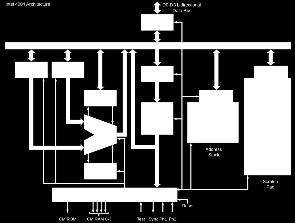
163 [

164 [
165 Intel's 8086 Chip [

166 [
; =main registers; 2=segment registers and IP; 3=address adder; 4=internal address")
167 [ Simplified block diagram of Intel 8088 (a variant of 8086); =main registers; 2=segment registers and IP; 3=address adder; 4=internal address bus; 5=instruction queue; 6=control unit (very simplified!); 7=bus interface; 8=internal databus; 9=ALU; 0//2=external address/ data/control bus.
168 Questions?
169 THE END
CprE 281: Digital Logic
 CprE 28: Digital Logic Instructor: Alexander Stoytchev http://www.ece.iastate.edu/~alexs/classes/ Decoders and Encoders CprE 28: Digital Logic Iowa State University, Ames, IA Copyright Alexander Stoytchev
Design of Sequential Circuits
 Design of Sequential Circuits Seven Steps: Construct a state diagram (showing contents of flip flop and inputs with next state) Assign letter variables to each flip flop and each input and output variable
CprE 281: Digital Logic
 CprE 281: Digital Logic Instructor: Alexander Stoytchev http://www.ece.iastate.edu/~alexs/classes/ Synchronous Sequential Circuits Basic Design Steps CprE 281: Digital Logic Iowa State University, Ames,
ECE 341. Lecture # 3
 ECE 341 Lecture # 3 Instructor: Zeshan Chishti zeshan@ece.pdx.edu October 7, 2013 Portland State University Lecture Topics Counters Finite State Machines Decoders Multiplexers Reference: Appendix A of
Combinational Logic. By : Ali Mustafa
 Combinational Logic By : Ali Mustafa Contents Adder Subtractor Multiplier Comparator Decoder Encoder Multiplexer How to Analyze any combinational circuit like this? Analysis Procedure To obtain the output
CprE 281: Digital Logic
 CprE 281: Digital Logic Instructor: Alexander Stoytchev http://www.ece.iastate.edu/~alexs/classes/ Fast Adders CprE 281: Digital Logic Iowa State University, Ames, IA Copyright Alexander Stoytchev HW5
Appendix B. Review of Digital Logic. Baback Izadi Division of Engineering Programs
 Appendix B Review of Digital Logic Baback Izadi Division of Engineering Programs bai@engr.newpaltz.edu Elect. & Comp. Eng. 2 DeMorgan Symbols NAND (A.B) = A +B NOR (A+B) = A.B AND A.B = A.B = (A +B ) OR
ALU A functional unit
 ALU A functional unit that performs arithmetic operations such as ADD, SUB, MPY logical operations such as AND, OR, XOR, NOT on given data types: 8-,16-,32-, or 64-bit values A n-1 A n-2... A 1 A 0 B n-1
Design at the Register Transfer Level
 Week-7 Design at the Register Transfer Level Algorithmic State Machines Algorithmic State Machine (ASM) q Our design methodologies do not scale well to real-world problems. q 232 - Logic Design / Algorithmic
Digital Logic: Boolean Algebra and Gates. Textbook Chapter 3
 Digital Logic: Boolean Algebra and Gates Textbook Chapter 3 Basic Logic Gates XOR CMPE12 Summer 2009 02-2 Truth Table The most basic representation of a logic function Lists the output for all possible
CprE 281: Digital Logic
 CprE 28: Digital Logic Instructor: Alexander Stoytchev http://www.ece.iastate.edu/~alexs/classes/ Code Converters CprE 28: Digital Logic Iowa State University, Ames, IA Copyright Alexander Stoytchev HW
Chapter 5. Digital Design and Computer Architecture, 2 nd Edition. David Money Harris and Sarah L. Harris. Chapter 5 <1>
 Chapter 5 Digital Design and Computer Architecture, 2 nd Edition David Money Harris and Sarah L. Harris Chapter 5 Chapter 5 :: Topics Introduction Arithmetic Circuits umber Systems Sequential Building
CPS 104 Computer Organization and Programming Lecture 11: Gates, Buses, Latches. Robert Wagner
 CPS 4 Computer Organization and Programming Lecture : Gates, Buses, Latches. Robert Wagner CPS4 GBL. RW Fall 2 Overview of Today s Lecture: The MIPS ALU Shifter The Tristate driver Bus Interconnections
Digital Logic. CS211 Computer Architecture. l Topics. l Transistors (Design & Types) l Logic Gates. l Combinational Circuits.
 l Logic Gates. l Combinational Circuits.") CS211 Computer Architecture Digital Logic l Topics l Transistors (Design & Types) l Logic Gates l Combinational Circuits l K-Maps Figures & Tables borrowed from:! http://www.allaboutcircuits.com/vol_4/index.html!
CS211 Computer Architecture Digital Logic l Topics l Transistors (Design & Types) l Logic Gates l Combinational Circuits l K-Maps Figures & Tables borrowed from:! http://www.allaboutcircuits.com/vol_4/index.html!
CprE 281: Digital Logic
 CprE 281: Digital Logic Instructor: Alexander Stoytchev http://www.ece.iastate.edu/~alexs/classes/ Signed Numbers CprE 281: Digital Logic Iowa State University, Ames, IA Copyright Alexander Stoytchev Administrative
ECE 250 / CPS 250 Computer Architecture. Basics of Logic Design Boolean Algebra, Logic Gates
 ECE 250 / CPS 250 Computer Architecture Basics of Logic Design Boolean Algebra, Logic Gates Benjamin Lee Slides based on those from Andrew Hilton (Duke), Alvy Lebeck (Duke) Benjamin Lee (Duke), and Amir
Arithme(c logic units and memory
 Arithme(c logic units and memory CSCI 255: Introduc/on to Embedded Systems Keith Vertanen Copyright 2011 Layers of abstrac-on abstrac(on building blocks examples computer components Macbook Pro components
EECS150 - Digital Design Lecture 11 - Shifters & Counters. Register Summary
 EECS50 - Digital Design Lecture - Shifters & Counters February 24, 2003 John Wawrzynek Spring 2005 EECS50 - Lec-counters Page Register Summary All registers (this semester) based on Flip-flops: q 3 q 2
Sample Test Paper - I
 Scheme G Sample Test Paper - I Course Name : Computer Engineering Group Marks : 25 Hours: 1 Hrs. Q.1) Attempt any THREE: 09 Marks a) Define i) Propagation delay ii) Fan-in iii) Fan-out b) Convert the following:
CSE140: Components and Design Techniques for Digital Systems. Decoders, adders, comparators, multipliers and other ALU elements. Tajana Simunic Rosing
 CSE4: Components and Design Techniques for Digital Systems Decoders, adders, comparators, multipliers and other ALU elements Tajana Simunic Rosing Mux, Demux Encoder, Decoder 2 Transmission Gate: Mux/Tristate
ECE/CS 250 Computer Architecture
 ECE/CS 250 Computer Architecture Basics of Logic Design: Boolean Algebra, Logic Gates (Combinational Logic) Tyler Bletsch Duke University Slides are derived from work by Daniel J. Sorin (Duke), Alvy Lebeck
Combinational Logic. Mantıksal Tasarım BBM231. section instructor: Ufuk Çelikcan
 Combinational Logic Mantıksal Tasarım BBM23 section instructor: Ufuk Çelikcan Classification. Combinational no memory outputs depends on only the present inputs expressed by Boolean functions 2. Sequential
Logic and Computer Design Fundamentals. Chapter 8 Sequencing and Control
 Logic and Computer Design Fundamentals Chapter 8 Sequencing and Control Datapath and Control Datapath - performs data transfer and processing operations Control Unit - Determines enabling and sequencing
CprE 281: Digital Logic
 CprE 281: Digital Logic Instructor: Alexander Stoytchev http://www.ece.iastate.edu/~alexs/classes/ Multiplication CprE 281: Digital Logic Iowa State University, Ames, IA Copyright Alexander Stoytchev HW
Logic. Combinational. inputs. outputs. the result. system can
 Digital Electronics Combinational Logic Functions Digital logic circuits can be classified as either combinational or sequential circuits. A combinational circuit is one where the output at any time depends
ELCT201: DIGITAL LOGIC DESIGN
 ELCT201: DIGITAL LOGIC DESIGN Dr. Eng. Haitham Omran, haitham.omran@guc.edu.eg Dr. Eng. Wassim Alexan, wassim.joseph@guc.edu.eg Lecture 5 Following the slides of Dr. Ahmed H. Madian ذو الحجة 1438 ه Winter
Lecture 7: Logic design. Combinational logic circuits
 /24/28 Lecture 7: Logic design Binary digital circuits: Two voltage levels: and (ground and supply voltage) Built from transistors used as on/off switches Analog circuits not very suitable for generic
Boolean Algebra and Digital Logic 2009, University of Colombo School of Computing
 IT 204 Section 3.0 Boolean Algebra and Digital Logic Boolean Algebra 2 Logic Equations to Truth Tables X = A. B + A. B + AB A B X 0 0 0 0 3 Sum of Products The OR operation performed on the products of
LOGIC CIRCUITS. Basic Experiment and Design of Electronics
 Basic Experiment and Design of Electronics LOGIC CIRCUITS Ho Kyung Kim, Ph.D. hokyung@pusan.ac.kr School of Mechanical Engineering Pusan National University Outline Combinational logic circuits Output
Lecture 13: Sequential Circuits, FSM
 Lecture 13: Sequential Circuits, FSM Today s topics: Sequential circuits Finite state machines 1 Clocks A microprocessor is composed of many different circuits that are operating simultaneously if each
Preparation of Examination Questions and Exercises: Solutions
 Questions Preparation of Examination Questions and Exercises: Solutions. -bit Subtraction: DIF = B - BI B BI BO DIF 2 DIF: B BI 4 6 BI 5 BO: BI BI 4 5 7 3 2 6 7 3 B B B B B DIF = B BI ; B = ( B) BI ( B),
Boolean Logic Continued Prof. James L. Frankel Harvard University
 Boolean Logic Continued Prof. James L. Frankel Harvard University Version of 10:18 PM 5-Sep-2017 Copyright 2017, 2016 James L. Frankel. All rights reserved. D Latch D R S Clk D Clk R S X 0 ~S 0 = R 0 ~R
課程名稱 : 數位邏輯設計 P-1/ /6/11
 課程名稱 : 數位邏輯設計 P-1/55 2012/6/11 Textbook: Digital Design, 4 th. Edition M. Morris Mano and Michael D. Ciletti Prentice-Hall, Inc. 教師 : 蘇慶龍 INSTRUCTOR : CHING-LUNG SU E-mail: kevinsu@yuntech.edu.tw Chapter
We are here. Assembly Language. Processors Arithmetic Logic Units. Finite State Machines. Circuits Gates. Transistors
 CSC258 Week 3 1 Logistics If you cannot login to MarkUs, email me your UTORID and name. Check lab marks on MarkUs, if it s recorded wrong, contact Larry within a week after the lab. Quiz 1 average: 86%
Digital Electronics II Mike Brookes Please pick up: Notes from the front desk
 NOTATION.PPT(10/8/2010) 1.1 Digital Electronics II Mike Brookes Please pick up: Notes from the front desk 1. What does Digital mean? 2. Where is it used? 3. Why is it used? 4. What are the important features
COMBINATIONAL LOGIC FUNCTIONS
 COMBINATIONAL LOGIC FUNCTIONS Digital logic circuits can be classified as either combinational or sequential circuits. A combinational circuit is one where the output at any time depends only on the present
CS61C : Machine Structures
 CS 61C L15 Blocks (1) inst.eecs.berkeley.edu/~cs61c/su05 CS61C : Machine Structures Lecture #15: Combinational Logic Blocks Outline CL Blocks Latches & Flip Flops A Closer Look 2005-07-14 Andy Carle CS
Fundamentals of Digital Design
 Fundamentals of Digital Design Digital Radiation Measurement and Spectroscopy NE/RHP 537 1 Binary Number System The binary numeral system, or base-2 number system, is a numeral system that represents numeric
ELEN Electronique numérique
 ELEN0040 - Electronique numérique Patricia ROUSSEAUX Année académique 2014-2015 CHAPITRE 3 Combinational Logic Circuits ELEN0040 3-4 1 Combinational Functional Blocks 1.1 Rudimentary Functions 1.2 Functions
Menu. Excitation Tables (Bonus Slide) EEL3701 EEL3701. Registers, RALU, Asynch, Synch
 EEL3701 EEL3701. Registers, RALU, Asynch, Synch") Menu Registers >Storage Registers >Shift Registers More LSI Components >Arithmetic-Logic Units (ALUs) > Carry-Look-Ahead Circuitry (skip this) Asynchronous versus Synchronous Look into my... 1 Excitation
Menu Registers >Storage Registers >Shift Registers More LSI Components >Arithmetic-Logic Units (ALUs) > Carry-Look-Ahead Circuitry (skip this) Asynchronous versus Synchronous Look into my... 1 Excitation
DE58/DC58 LOGIC DESIGN DEC 2014
 Q.2 a. In a base-5 number system, 3 digit representations is used. Find out (i) Number of distinct quantities that can be represented.(ii) Representation of highest decimal number in base-5. Since, r=5
CS61C : Machine Structures
 inst.eecs.berkeley.edu/~cs61c/su05 CS61C : Machine Structures Lecture #15: Combinational Logic Blocks 2005-07-14 CS 61C L15 Blocks (1) Andy Carle Outline CL Blocks Latches & Flip Flops A Closer Look CS
Adders, subtractors comparators, multipliers and other ALU elements
 CSE4: Components and Design Techniques for Digital Systems Adders, subtractors comparators, multipliers and other ALU elements Adders 2 Circuit Delay Transistors have instrinsic resistance and capacitance
Sequential Circuits. CS/EE 3700 : Fundamentals of Digital System Design
 Sequential Circuits CS/EE 37 : Fundamentals of igital System esign Chris J. Myers Lecture 7: Flip-flops, Registers, Counters Chapter 7 Combinational output depends only on the input. Sequential output
VHDL DESIGN AND IMPLEMENTATION OF C.P.U BY REVERSIBLE LOGIC GATES
 VHDL DESIGN AND IMPLEMENTATION OF C.P.U BY REVERSIBLE LOGIC GATES 1.Devarasetty Vinod Kumar/ M.tech,2. Dr. Tata Jagannadha Swamy/Professor, Dept of Electronics and Commn. Engineering, Gokaraju Rangaraju
Unit II Chapter 4:- Digital Logic Contents 4.1 Introduction... 4
 Unit II Chapter 4:- Digital Logic Contents 4.1 Introduction... 4 4.1.1 Signal... 4 4.1.2 Comparison of Analog and Digital Signal... 7 4.2 Number Systems... 7 4.2.1 Decimal Number System... 7 4.2.2 Binary
Adders, subtractors comparators, multipliers and other ALU elements
 CSE4: Components and Design Techniques for Digital Systems Adders, subtractors comparators, multipliers and other ALU elements Instructor: Mohsen Imani UC San Diego Slides from: Prof.Tajana Simunic Rosing
Section 3: Combinational Logic Design. Department of Electrical Engineering, University of Waterloo. Combinational Logic
 Section 3: Combinational Logic Design Major Topics Design Procedure Multilevel circuits Design with XOR gates Adders and Subtractors Binary parallel adder Decoders Encoders Multiplexers Programmed Logic
Fundamentals of Computer Systems
 Fundamentals of Computer Systems Review for the Final Stephen A. Edwards Columbia University Summer 25 The Final 2 hours 8 problems Closed book Simple calculators are OK, but unnecessary One double-sided
ECEN 248: INTRODUCTION TO DIGITAL SYSTEMS DESIGN. Week 9 Dr. Srinivas Shakkottai Dept. of Electrical and Computer Engineering
 ECEN 248: INTRODUCTION TO DIGITAL SYSTEMS DESIGN Week 9 Dr. Srinivas Shakkottai Dept. of Electrical and Computer Engineering TIMING ANALYSIS Overview Circuits do not respond instantaneously to input changes
Latches. October 13, 2003 Latches 1
 Latches The second part of CS231 focuses on sequential circuits, where we add memory to the hardware that we ve already seen. Our schedule will be very similar to before: We first show how primitive memory
Review for Final Exam
 CSE140: Components and Design Techniques for Digital Systems Review for Final Exam Mohsen Imani CAPE Please submit your evaluations!!!! RTL design Use the RTL design process to design a system that has
UNIVERSITY OF WISCONSIN MADISON
 CS/ECE 252: INTRODUCTION TO COMPUTER ENGINEERING UNIVERSITY OF WISCONSIN MADISON Prof. Gurindar Sohi TAs: Minsub Shin, Lisa Ossian, Sujith Surendran Midterm Examination 2 In Class (50 minutes) Friday,
LOGIC CIRCUITS. Basic Experiment and Design of Electronics. Ho Kyung Kim, Ph.D.
 Basic Experiment and Design of Electronics LOGIC CIRCUITS Ho Kyung Kim, Ph.D. hokyung@pusan.ac.kr School of Mechanical Engineering Pusan National University Digital IC packages TTL (transistor-transistor
CMP 334: Seventh Class
 CMP 334: Seventh Class Performance HW 5 solution Averages and weighted averages (review) Amdahl's law Ripple-carry adder circuits Binary addition Half-adder circuits Full-adder circuits Subtraction, negative
Logic. Basic Logic Functions. Switches in series (AND) Truth Tables. Switches in Parallel (OR) Alternative view for OR
 Truth Tables. Switches in Parallel (OR) Alternative view for OR") TOPIS: Logic Logic Expressions Logic Gates Simplifying Logic Expressions Sequential Logic (Logic with a Memory) George oole (85-864), English mathematician, oolean logic used in digital computers since
TOPIS: Logic Logic Expressions Logic Gates Simplifying Logic Expressions Sequential Logic (Logic with a Memory) George oole (85-864), English mathematician, oolean logic used in digital computers since
Figure 4.9 MARIE s Datapath
 Term Control Word Microoperation Hardwired Control Microprogrammed Control Discussion A set of signals that executes a microoperation. A register transfer or other operation that the CPU can execute in
Binary addition example worked out
 Binary addition example worked out Some terms are given here Exercise: what are these numbers equivalent to in decimal? The initial carry in is implicitly 0 1 1 1 0 (Carries) 1 0 1 1 (Augend) + 1 1 1 0
SAU1A FUNDAMENTALS OF DIGITAL COMPUTERS
 SAU1A FUNDAMENTALS OF DIGITAL COMPUTERS Unit : I - V Unit : I Overview Fundamentals of Computers Characteristics of Computers Computer Language Operating Systems Generation of Computers 2 Definition of
SIR C.R.REDDY COLLEGE OF ENGINEERING ELURU DIGITAL INTEGRATED CIRCUITS (DIC) LABORATORY MANUAL III / IV B.E. (ECE) : I - SEMESTER
 LABORATORY MANUAL III / IV B.E. (ECE) : I - SEMESTER") SIR C.R.REDDY COLLEGE OF ENGINEERING ELURU 534 007 DIGITAL INTEGRATED CIRCUITS (DIC) LABORATORY MANUAL III / IV B.E. (ECE) : I - SEMESTER DEPARTMENT OF ELECTRONICS AND COMMUNICATION ENGINEERING DIGITAL
SIR C.R.REDDY COLLEGE OF ENGINEERING ELURU 534 007 DIGITAL INTEGRATED CIRCUITS (DIC) LABORATORY MANUAL III / IV B.E. (ECE) : I - SEMESTER DEPARTMENT OF ELECTRONICS AND COMMUNICATION ENGINEERING DIGITAL
BER KELEY D AV IS IR VINE LOS AN GELES RIVERS IDE SAN D IEGO S AN FRANCISCO
 UN IVERSIT Y O F CA LIFO RNI A AT BERKELEY BER KELEY D AV IS IR VINE LOS AN GELES RIVERS IDE SAN D IEGO S AN FRANCISCO SAN TA BARBA RA S AN TA CRUZ De p a r tm en t of Ele ctr i ca l En gin e e rin g a
INF2270 Spring Philipp Häfliger. Lecture 8: Superscalar CPUs, Course Summary/Repetition (1/2)
") INF2270 Spring 2010 Philipp Häfliger Summary/Repetition (1/2) content From Scalar to Superscalar Lecture Summary and Brief Repetition Binary numbers Boolean Algebra Combinational Logic Circuits Encoder/Decoder
INF2270 Spring 2010 Philipp Häfliger Summary/Repetition (1/2) content From Scalar to Superscalar Lecture Summary and Brief Repetition Binary numbers Boolean Algebra Combinational Logic Circuits Encoder/Decoder
Chapter 4. Combinational: Circuits with logic gates whose outputs depend on the present combination of the inputs. elements. Dr.
 Chapter 4 Dr. Panos Nasiopoulos Combinational: Circuits with logic gates whose outputs depend on the present combination of the inputs. Sequential: In addition, they include storage elements Combinational
EECS150 - Digital Design Lecture 25 Shifters and Counters. Recap
 EECS150 - Digital Design Lecture 25 Shifters and Counters Nov. 21, 2013 Prof. Ronald Fearing Electrical Engineering and Computer Sciences University of California, Berkeley (slides courtesy of Prof. John
Systems I: Computer Organization and Architecture
 Systems I: Computer Organization and Architecture Lecture 6 - Combinational Logic Introduction A combinational circuit consists of input variables, logic gates, and output variables. The logic gates accept
CPE100: Digital Logic Design I
 Professor Brendan Morris, SEB 3216, brendan.morris@unlv.edu CPE100: Digital Logic Design I Final Review http://www.ee.unlv.edu/~b1morris/cpe100/ 2 Logistics Tuesday Dec 12 th 13:00-15:00 (1-3pm) 2 hour
UNIT 8A Computer Circuitry: Layers of Abstraction. Boolean Logic & Truth Tables
 UNIT 8 Computer Circuitry: Layers of bstraction 1 oolean Logic & Truth Tables Computer circuitry works based on oolean logic: operations on true (1) and false (0) values. ( ND ) (Ruby: && ) 0 0 0 0 0 1
Introduction to Computer Engineering. CS/ECE 252, Fall 2012 Prof. Guri Sohi Computer Sciences Department University of Wisconsin Madison
 Introduction to Computer Engineering CS/ECE 252, Fall 2012 Prof. Guri Sohi Computer Sciences Department University of Wisconsin Madison Chapter 3 Digital Logic Structures Slides based on set prepared by
Digital Integrated Circuits A Design Perspective. Arithmetic Circuits. Jan M. Rabaey Anantha Chandrakasan Borivoje Nikolic.
 Digital Integrated Circuits A Design Perspective Jan M. Rabaey Anantha Chandrakasan Borivoje Nikolic Arithmetic Circuits January, 2003 1 A Generic Digital Processor MEMORY INPUT-OUTPUT CONTROL DATAPATH
CMPE12 - Notes chapter 2. Digital Logic. (Textbook Chapters and 2.1)"
") CMPE12 - Notes chapter 2 Digital Logic (Textbook Chapters 3.1-3.5 and 2.1)" Truth table" The most basic representation of a logic function." Brute force representation listing the output for all possible
CMPE12 - Notes chapter 2 Digital Logic (Textbook Chapters 3.1-3.5 and 2.1)" Truth table" The most basic representation of a logic function." Brute force representation listing the output for all possible
Combinational Logic Design Combinational Functions and Circuits
 Combinational Logic Design Combinational Functions and Circuits Overview Combinational Circuits Design Procedure Generic Example Example with don t cares: BCD-to-SevenSegment converter Binary Decoders
DIGITAL TECHNICS. Dr. Bálint Pődör. Óbuda University, Microelectronics and Technology Institute
 DIGITAL TECHNICS Dr. Bálint Pődör Óbuda University, Microelectronics and Technology Institute 4. LECTURE: COMBINATIONAL LOGIC DESIGN: ARITHMETICS (THROUGH EXAMPLES) 2016/2017 COMBINATIONAL LOGIC DESIGN:
ECE 545 Digital System Design with VHDL Lecture 1. Digital Logic Refresher Part A Combinational Logic Building Blocks
 ECE 545 Digital System Design with VHDL Lecture Digital Logic Refresher Part A Combinational Logic Building Blocks Lecture Roadmap Combinational Logic Basic Logic Review Basic Gates De Morgan s Law Combinational
Verilog HDL:Digital Design and Modeling. Chapter 11. Additional Design Examples. Additional Figures
 Chapter Additional Design Examples Verilog HDL:Digital Design and Modeling Chapter Additional Design Examples Additional Figures Chapter Additional Design Examples 2 Page 62 a b y y 2 y 3 c d e f Figure
Chapter 5 Arithmetic Circuits
 Chapter 5 Arithmetic Circuits SKEE2263 Digital Systems Mun im/ismahani/izam {munim@utm.my,e-izam@utm.my,ismahani@fke.utm.my} February 11, 2016 Table of Contents 1 Iterative Designs 2 Adders 3 High-Speed
Logic Design II (17.342) Spring Lecture Outline
 Spring Lecture Outline") Logic Design II (17.342) Spring 2012 Lecture Outline Class # 10 April 12, 2012 Dohn Bowden 1 Today s Lecture First half of the class Circuits for Arithmetic Operations Chapter 18 Should finish at least
Logic Design II (17.342) Spring 2012 Lecture Outline Class # 10 April 12, 2012 Dohn Bowden 1 Today s Lecture First half of the class Circuits for Arithmetic Operations Chapter 18 Should finish at least
Chapter 3 Digital Logic Structures
 Chapter 3 Digital Logic Structures Original slides from Gregory Byrd, North Carolina State University Modified by C. Wilcox, M. Strout, Y. Malaiya Colorado State University Computing Layers Problems Algorithms
Fundamentals of Computer Systems
 Fundamentals of Computer Systems Review for the Midterm Stephen A. Edwards Columbia University Spring 22 The Midterm 75 minutes 4 5 problems Closed book Simple calculators are OK, but unnecessary One double-sided
Appendix A: Digital Logic. Principles of Computer Architecture. Principles of Computer Architecture by M. Murdocca and V. Heuring
 - Principles of Computer rchitecture Miles Murdocca and Vincent Heuring 999 M. Murdocca and V. Heuring -2 Chapter Contents. Introduction.2 Combinational Logic.3 Truth Tables.4 Logic Gates.5 Properties
Introduction to Digital Logic Missouri S&T University CPE 2210 Subtractors
 Introduction to Digital Logic Missouri S&T University CPE 2210 Egemen K. Çetinkaya Egemen K. Çetinkaya Department of Electrical & Computer Engineering Missouri University of Science and Technology cetinkayae@mst.edu
S.Y. Diploma : Sem. III [CO/CM/IF/CD/CW] Digital Techniques
![S.Y. Diploma : Sem. III [CO/CM/IF/CD/CW] Digital Techniques](/thumbs/90/103932933.jpg "S.Y. Diploma : Sem. III [CO/CM/IF/CD/CW] Digital Techniques") S.Y. Diploma : Sem. III [CO/CM/IF/CD/CW] Digital Techniques Time: 3 Hrs.] Prelim Question Paper Solution [Marks : 100 Q.1(a) Attempt any SIX of the following : [12] Q.1(a) (i) Derive AND gate and OR gate
S.Y. Diploma : Sem. III [CO/CM/IF/CD/CW] Digital Techniques Time: 3 Hrs.] Prelim Question Paper Solution [Marks : 100 Q.1(a) Attempt any SIX of the following : [12] Q.1(a) (i) Derive AND gate and OR gate
SRC Language Conventions. Class 6: Intro to SRC Simulator Register Transfers and Logic Circuits. SRC Simulator Demo. cond_br.asm.
 Fall 2006 S333: omputer rchitecture University of Virginia omputer Science Michele o SR Language onventions lass 6: Intro to SR Simulator Register Transfers and Logic ircuits hapter 2, ppendix.5 2 SR Simulator
CSC 322: Computer Organization Lab
 CSC 322: Computer Organization Lab Lecture 3: Logic Design Dr. Haidar M. Harmanani CSC 322: Computer Organization Lab Part I: Combinational Logic Dr. Haidar M. Harmanani Logical Design of Digital Systems
Topic 8: Sequential Circuits
 Topic 8: Sequential Circuits Readings : Patterson & Hennesy, Appendix B.4 - B.6 Goals Basic Principles behind Memory Elements Clocks Applications of sequential circuits Introduction to the concept of the
Introduction EE 224: INTRODUCTION TO DIGITAL CIRCUITS & COMPUTER DESIGN. Lecture 6: Sequential Logic 3 Registers & Counters 5/9/2010
 EE 224: INTROUCTION TO IGITAL CIRCUITS & COMPUTER ESIGN Lecture 6: Sequential Logic 3 Registers & Counters 05/10/2010 Avinash Kodi, kodi@ohio.edu Introduction 2 A Flip-Flop stores one bit of information
ECE 2300 Digital Logic & Computer Organization
 ECE 23 Digital Logic & Computer Organization Spring 28 Combinational Building Blocks Lecture 5: Announcements Lab 2 prelab due tomorrow HW due Friday HW 2 to be posted on Thursday Lecture 4 to be replayed
Spiral 2-1. Datapath Components: Counters Adders Design Example: Crosswalk Controller
 2-. piral 2- Datapath Components: Counters s Design Example: Crosswalk Controller 2-.2 piral Content Mapping piral Theory Combinational Design equential Design ystem Level Design Implementation and Tools
Digital Logic Appendix A
 Digital Logic Appendix A Boolean Algebra Gates Combinatorial Circuits Sequential Circuits 1 Boolean Algebra George Boole ideas 1854 Claude Shannon, apply to circuit design, 1938 Describe digital circuitry
CMPEN 411 VLSI Digital Circuits Spring Lecture 19: Adder Design
 CMPEN 411 VLSI Digital Circuits Spring 2011 Lecture 19: Adder Design [Adapted from Rabaey s Digital Integrated Circuits, Second Edition, 2003 J. Rabaey, A. Chandrakasan, B. Nikolic] Sp11 CMPEN 411 L19
EECS150 - Digital Design Lecture 18 - Counters
 EECS150 - Digital Design Lecture 18 - Counters October 24, 2002 John Wawrzynek Fall 2002 EECS150 - Lec18-counters Page 1 Counters Special sequential circuits (FSMs) that sequence though a set outputs.
EECS150 - Digital Design Lecture 18 - Counters
 EECS50 - Digital Design Lecture 8 - Counters October 24, 2002 John Wawrzynek Fall 2002 EECS50 - Lec8-counters Page Counters Special sequential circuits (FSMs) that sequence though a set outputs. Examples:
Combinational Logic Trainer Lab Manual
 Combinational Logic Trainer Lab Manual Control Inputs Microprocessor Data Inputs ff Control Unit '0' Datapath MUX Nextstate Logic State Memory Register Output Logic Control Signals ALU ff Register Status
Digital Integrated Circuits A Design Perspective. Arithmetic Circuits. Jan M. Rabaey Anantha Chandrakasan Borivoje Nikolic.
 Digital Integrated Circuits A Design Perspective Jan M. Rabaey Anantha Chandrakasan Borivoje Nikolic Arithmetic Circuits January, 2003 1 A Generic Digital Processor MEM ORY INPUT-OUTPUT CONTROL DATAPATH
CMSC 313 Lecture 25 Registers Memory Organization DRAM
 CMSC 33 Lecture 25 Registers Memory Organization DRAM UMBC, CMSC33, Richard Chang A-75 Four-Bit Register Appendix A: Digital Logic Makes use of tri-state buffers so that multiple registers
EE40 Lec 15. Logic Synthesis and Sequential Logic Circuits
 EE40 Lec 15 Logic Synthesis and Sequential Logic Circuits Prof. Nathan Cheung 10/20/2009 Reading: Hambley Chapters 7.4-7.6 Karnaugh Maps: Read following before reading textbook http://www.facstaff.bucknell.edu/mastascu/elessonshtml/logic/logic3.html
Number Systems 1(Solutions for Vol 1_Classroom Practice Questions)
") Chapter Number Systems (Solutions for Vol _Classroom Practice Questions). ns: (d) 5 x + 44 x = x ( x + x + 5 x )+( x +4 x + 4 x ) = x + x + x x +x+5+x +4x+4 = x + x + x 5x 6 = (x6) (x+ ) = (ase cannot
Chapter Number Systems (Solutions for Vol _Classroom Practice Questions). ns: (d) 5 x + 44 x = x ( x + x + 5 x )+( x +4 x + 4 x ) = x + x + x x +x+5+x +4x+4 = x + x + x 5x 6 = (x6) (x+ ) = (ase cannot
Digital Circuits. 1. Inputs & Outputs are quantized at two levels. 2. Binary arithmetic, only digits are 0 & 1. Position indicates power of 2.
 Digital Circuits 1. Inputs & Outputs are quantized at two levels. 2. inary arithmetic, only digits are 0 & 1. Position indicates power of 2. 11001 = 2 4 + 2 3 + 0 + 0 +2 0 16 + 8 + 0 + 0 + 1 = 25 Digital
Table of Content. Chapter 11 Dedicated Microprocessors Page 1 of 25
 Chapter 11 Dedicated Microprocessors Page 1 of 25 Table of Content Table of Content... 1 11 Dedicated Microprocessors... 2 11.1 Manual Construction of a Dedicated Microprocessor... 3 11.2 FSM + D Model
Floating Point Representation and Digital Logic. Lecture 11 CS301
 Floating Point Representation and Digital Logic Lecture 11 CS301 Administrative Daily Review of today s lecture w Due tomorrow (10/4) at 8am Lab #3 due Friday (9/7) 1:29pm HW #5 assigned w Due Monday 10/8
King Fahd University of Petroleum and Minerals College of Computer Science and Engineering Computer Engineering Department
 King Fahd University of Petroleum and Minerals College of Computer Science and Engineering Computer Engineering Department Page of COE 22: Digital Logic Design (3--3) Term (Fall 22) Final Exam Sunday January