Combinational Logic. Mantıksal Tasarım BBM231. section instructor: Ufuk Çelikcan
|
|
|
- Jonathan Norton
- 6 years ago
- Views:
Transcription
1 Combinational Logic Mantıksal Tasarım BBM23 section instructor: Ufuk Çelikcan
2 Classification. Combinational no memory outputs depends on only the present inputs expressed by Boolean functions 2. Sequential storage elements + logic gates the content of the storage elements define the state of the circuit outputs are functions of both input and current state state is a function of previous inputs outputs not only depend the present inputs but also the past inputs 2
3 Combinational Circuits n binary inputs Combinational circuit (logic gates) m binary outputs 3 n input bits 2 n possible binary input combinations For each possible input combination, there is one possible output value truth table Boolean functions (with n input variables) Examples: adders, subtractors, comparators, decoders, encoders, multiplexers.
4 Analysis & Design of Combinational Logic Analysis: to find out the function that a given circuit implements We are given a logic circuit and we are expected to find out. Boolean function(s) 2. Truth table 3. A possible explanation of the circuit operation (i.e. what it does) 4
5 Analysis of Combinational Logic First, make sure that the given circuit is, indeed, combinational. Verifying the circuit is combinational No memory elements No feedback paths (connections) Second, obtain a Boolean function for each output or the truth table Finally, interpret the operation of the circuit from the derived Boolean functions or truth table What is it the circuit doing? Addition, subtraction, multiplication, comparison etc. 5
6 Example Obtaining Boolean Function a b c T F a b c T 2 T 4 a b T 3 a c F 2 b c 6
7 Example: Obtaining Boolean Function Boolean expressions for named wires T = abc T 2 = a + b + c F 2 = T 3 = T 4 = T 3 T 2 F = T + T 4 = = = = 7
8 Example: Obtaining Boolean Function Boolean expressions for named wires T = abc T 2 = a + b + c F 2 = ab + ac + bc T 3 = F 2 = (ab + ac + bc) T 4 = T 3 T 2 = (ab + ac + bc) (a + b + c) F = T + T 4 = abc + (ab + ac + bc) (a + b + c) = abc + ((a + b )(a + c )(b + c )) (a + b + c) = abc + ( (a + a c + a b + b c )(b + c ) ) (a + b + c) = abc + (a b + a c + a b c + b c ) (a + b + c) = abc + (a b + a c + b c ) (a + b + c) 8
9 Example: Obtaining Boolean Function Boolean expressions for outputs F 2 = ab + ac + bc F = F = F = F = 9
10 Example: Obtaining Boolean Function Boolean expressions for outputs F 2 = ab + ac + bc F = abc + (a b + a c + b c ) (a + b + c) F = abc + a b c + a bc + ab c F = a(bc + b c ) + a (b c + bc ) F = a(b c) + a (b c) F = ( a b c ) : Odd Function
11 Example: Obtaining Truth Table F = a b c F 2 = ab + ac + bc carry sum a b c T T 2 T 3 T 4 F 2 F
12 Example: Obtaining Truth Table F = a b c F 2 = ab + ac + bc carry sum a b c T T 2 T 3 T 4 F 2 F This is what we call full-adder (FA) 2
13 3 Design of Combinational Logic Design Procedure: We start with the verbal specification about what the resulting circuit will do for us (i.e. which function it will implement) Specifications are often verbal, and very likely incomplete and ambiguous (if not even faulty) Wrong interpretations can result in incorrect circuit We are expected to find. First, Boolean function(s) (or truth table) to realize the desired functionality 2. Logic circuit implementing the Boolean function(s) (or the truth table)
14 Possible Design Steps. Find out the number of inputs and outputs 2. Derive the truth table that defines the required relationship between inputs and outputs 3. Obtain a simplified Boolean function for each output 4. Draw the logic diagram (enter your design into CAD) 5. Verify the correctness of the design 4
15 Design Constraints From the truth table, we can obtain a variety of simplified expressions, all realizing the same function. Question: which one to choose? The design constraints may help in the selection process Constraints: number of gates propagation time of the signal all the way from the inputs to the outputs number of inputs to a gate number of interconnections power consumption driving capability of each gate 5
16 Example: Design Process BCD-to-242 Converter Verbal specification: Given a BCD digit (i.e. {,,, 9}), the circuit computes 242 code equivalent of the decimal number Step : how many inputs and how many outputs? four inputs and four outputs Step 2: Obtain the truth table etc. 6
17 BCD-to-242 Converter Truth Table Inputs Outputs A B C D x y z t 7
18 Binary coded decimal (BCD) is a system of writing numerals that assigns a fourdigit binary code to each digit through 9 in a decimal (base-) numeral. The fourbit BCD code for any particular single base- digit is its representation in binary notation, as follows: = = 2 = 3 = 4 = 5 = 6 = 7 = 8 = 9 = Numbers larger than 9, having two or more digits in the decimal system, are expressed digit by digit. For example, the BCD rendition of the base- number 895 is
19 242 Code a weighted code. The weights assigned to the four digits are 2, 4, 2, and. The 242 code is the same as that in BCD from to 4; however, it varies from 5 to 9. For example, in this case the bit combination represents decimal 4; whereas the bit combination is interpreted as the decimal 7, as obtained from = 7. This is also a self-complementarycode, that is, the 9 s complement of the decimal number is obtained by changing the s to s and s to s.
20 BCD-to-242 Converter Truth Table Inputs Outputs A B C D x y z t 2
21 BCD-to-242 Converter Truth Table Inputs Outputs A B C D x y z t 2
22 BCD-to-242 Converter Step 3: Obtain simplified Boolean expression for each output Output x: AB CD A B C D x The rest X x = 22
23 BCD-to-242 Converter Step 3: Obtain simplified Boolean expression for each output Output x: AB CD x x x x x x A B C D x The rest X 23
24 BCD-to-242 Converter Step 3: Obtain simplified Boolean expression for each output Output x: AB CD x x x x x x A B C D x The rest X x = BD + BC + A 24
25 CD 25 Boolean Expressions for Outputs AB CD AB Output y: Output z: A B C D y z y = z = The rest X X
26 CD 26 Boolean Expressions for Outputs AB X X X X X X CD Output y: Output z: AB X X X X X X A B C D y z y = z = The rest X X
27 CD 27 Boolean Expressions for Outputs AB X X X X X X CD Output y: Output z: AB X X X X X X A B C D y z The rest X X y = A + BD + BC z = A + B C + BC D
28 Boolean Expressions for Outputs CD Output t: AB A B C D T t = The rest X
29 Boolean Expressions for Outputs CD Output t: AB X X X X X X t = A B C D T Step 4: Draw the logic diagram x = BC + BD + A y = A + BD + BC z = A + B C + BC D The rest X 29
30 Boolean Expressions for Outputs CD Output t: AB X X X X X X t = D A B C D T Step 4: Draw the logic diagram x = BC + BD + A y = A + BD + BC z = A + B C + BC D The rest X 3
31 Example: Logic Diagram A B C D x = BC + BD + A y = A + BD + BC z = A + B C + BC D 3 t = D
32 Example: Verification Step 5: Check the functional correctness of the logic circuit Apply all possible input combinations And check if the circuit generates the correct outputs for each input combinations For large circuits with many input combinations, this may not be feasible. Statistical techniques may be used to verify the correctness of large circuits with many input combinations 32
33 Binary Adder/Subtractor (Arithmetic) Addition of two binary digits + =, + =, + =, and + = The result has two components the sum (S) the carry (C) (Arithmetic) Addition of three binary digits = + + = + + = + + = + + = + + = + + = + + =
34 Half Adder Truth table x y C S S = x y + xy = x y C = xy x y S HA C 34
35 Full Adder /2 A circuit that performs the arithmetic sum of three bits Three inputs the range of output is [, 3] Two binary outputs 35 x y z C S
36 Karnaugh Maps Full Adder 2/2 yz x yz x S =? C =? Two level implementation st level: three AND gates 2 nd level: One OR gate 36
37 Karnaugh Maps Full Adder 2/2 yz x yz x S = xy z + x y z + xyz + x yz =... =... = x y z C = xy + xz + yz = xyz + xyz + xy z + x yz Two level implementation st level: three AND gates 2 nd level: One OR gate 37
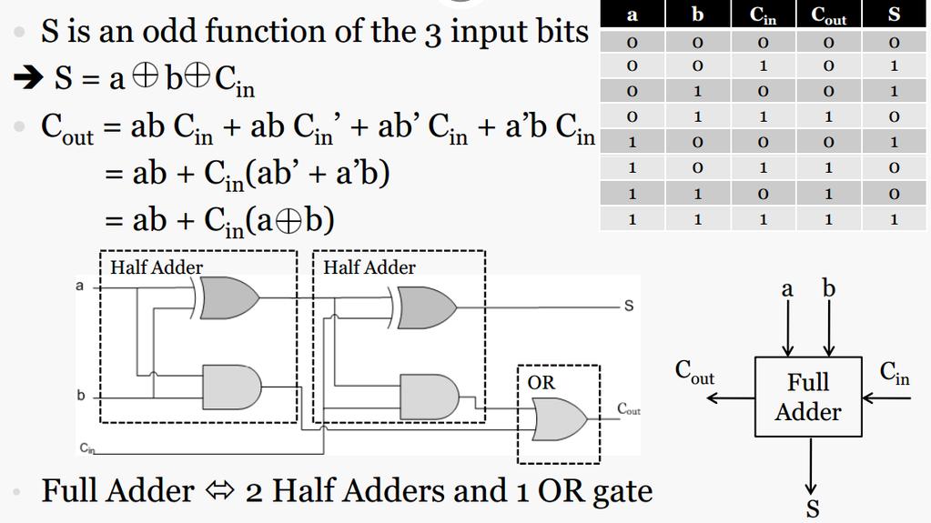
38
39 Full Adder: Hierarchical Realization Sum S = x y z = (x y) z Carry C = xyz + xyz + xy z + x yz = xy + (xy + x y) z = xy + (x y) z This allows us to implement a full-adder using two half adders. x y HA S C HA S C x y z = S C z 39
40 Full Adder Using Half Adders x y HA HA S z C 4
41 Integer Addition /2 Binary adder: A digital circuit that produces the arithmetic sum of two binary numbers A = (a n-, a n-2,, a, a ) B = (b n-, b n-2,, b, b ) A simple case: 4-bit binary adder a 3 b 3 a 2 b 2 a b a b C 4 C x FA S y z C 3 C x FA S y z C 2 C x FA S y z C C x HA S y S 3 S 2 S S 4
42 Integer Addition 2/2 a 3 b 3 a 2 b 2 a b a b C 4 C x FA S y z C 3 C x FA S y z C 2 C x FA S y z C C x FA S y z C = S 3 S 2 S S Ripple-carry adder 42
43 Hierarchical Design Methodology The design methodology we used to build carry-ripple adder is what is referred as hierarchical design. In classical design, we have: 9 inputs including C. 5 outputs Truth tables with 2 9 = 52 entries We have to optimize five Boolean functions with 9 variables each. Hierarchical design we divide our design into smaller functional blocks connect functional units to produce the big functionality 43

44 44 Full Adder in Xilinx

45 45 Two-bit Adder in Xilinx
46 Subtractor Recall how we do subtraction (2 s complement) X Y = X + (2 n Y) = X + ~Y + x 3 y 3 x 2 y 2 x y x y logic- a 3 b 3 a 2 b 2 a b a b C 4 4-bit adder circuit C S 3 S 2 S S C 4 46 S 3 S 2 S S
47 Carry Propagation a 3 b 3 a 2 b 2 a b a b C 4 C x FA S y z C 3 C x FA S y z C 2 C x FA S y z C C x FA S y z C = S 3 S 2 S S Ripple-carry adder What is the total propagation time of 4-bit ripple-carry adder? FA : propagation time of a single full adder. We have four full adders connected in cascaded fashion Total propagation time:?? 47
48 Carry Propagation Propagation time of a full adder XOR 2 AND = 2 OR FA 2 XOR a i P i b i S i G i C i+ C i 48 carry-propagate: carry-generate:

49 Carry Propagation a 3 b 3 a 2 b 2 a b a b C C 3 P P 3 C 2 2 C P P C 4 S3 C 3 S2 C 2 S C S Carry-lookahead design 49
50 Carry Propagation a 3 b 3 a 2 b 2 a b a b C C 3 P P 3 C 2 2 C P P C 4 S3 C 3 Delays P, P, P 2, P 3 : XOR 2 AND S2 C 2 S C S 5 C (S ): 2 AND C 2 (S ): 4 AND C 3 (S 2 ): 6 AND C 4 (S 3 ): 8 AND + 2 AND 4 AND + 2 AND 6 AND + 2 AND 8 AND + 2 AND AND
51 4-bit Carry Lookahead Adder a 3 b 3 P 3 C 4 C 4 G 3 a 2 b 2 P 2 C 3 P 3 S 3 a b G 2 P Carry Lookahead circuit C 2 P 2 P S S 2 G 2 C a b P G C P S C C 5
52 Decoders A binary code of n bits capable of representing 2 n distinct elements of coded information A decoder is a combinational circuit that converts binary information from n binary inputs to a maximum of 2 n unique output lines x y 2x4 decoder d d d 2 d 3 x y d d d 2 d 3 d = d = d 2 = d 3 = 52
53 Decoder with Enable Input x y 2x4 decoder d d d 2 d 3 e e x y d d d 2 d 3 X X 53
54 Demultiplexer A demultiplexer is a combinational circuit it receives information from a single input line and directs it one of 2 n output lines It has n selection lines as to which output will get the input x y 2x4 decoder d d d 2 d 3 x, y e d d d 2 d 3 e d = e when x = and y = d = e when x = and y = d 2 = e when x = and y = d 3 = e when x = and y = 56
55 Demultiplexer e x x 57
56 Demultiplexer e x2 x x 58
57 Demultiplexer x 59
58 Combining Decoders y z x 2x4 decoder e d d d 2 d 3 x y z active output 2x4 decoder e d 4 d 5 d 6 d 7 Decoders with enable inputs can be connected together to form a larger decoder circuit. Figure shows two 2-to-4-line decoders with enable inputs connected to form a 3-to-8-line decoder. When x=, the top decoder is enabled and the other is disabled. The bottom decoder outputs are all s, and the top four outputs generate minterms to. When x=, the enable conditions are reversed: The bottom decoder outputs generate minterms to, while the outputs of the top decoder are all s. This example demonstrates the usefulness of enable inputs in decoders
59 Combining Decoders x x n- nx2 n Decoder- e d d d 2 n - nx2 n Decoder-2 e nx2 n Decoder-2 p e d 2 n+p- - x n x n+p- px2 p Decoder 6
60 Decoder as a Building Block A decoder provides the 2 n minterms of n input variable x y 2x4 decoder d = x y d = x y d 2 = xy d 3 = xy We can use a decoder and OR gates to realize any Boolean function expressed as sum of minterms Any combinational circuit with n inputs and m outputs can be realized using an n-to-2 n line decoder and m OR gates. 62
61 Decoder as a Building Block-ROM x y z 3x8 decoder d = x y z d = x y z d 2 = x yz d 3 = x yz d 4 = xy z d 5 = xy z d 6 = xyz d 7 = xyz F 2 F F 63
62 Decoder as a Building Block-ROM x y z 3x8 decoder F 2 F F 64
63 Example: Decoder as a Building Block Full adder C = xy + xz + yz S = x y z x y z 3x8 decoder C S 65
64 Encoders An encoder is a combinational circuit that performs the inverse operation of a decoder number of inputs: 2 n number of outputs: n the output lines generate the binary code corresponding to the input value Example: n = 2 d d d 2 d 3 x y 66
65 Priority Encoder Problem with a regular encoder: only one input can be active at any given time the output is undefined for the case when more than one input is active simultaneously. Priority encoder: there is a priority among the inputs d d d 2 d 3 a b V X X X X X X X X 67
66 Priority Encoder if two or more inputs are equal to at the same time, the input having the highest priority will take precedence. In addition to the two outputs a and b, the circuit has a third output designated by V ; this is a valid bit indicator that is set to when one or more inputs are equal to. If all inputs are, there is no valid input and V is equal to. The other two outputs are not inspected when V equals and are specified as don t-care conditions. Priority encoder: d d d 2 d 3 a b V X X X X X X X X 68
67 4-bit Priority Encoder In the truth table X for input variables represents both and. Good for condensing the truth table Example: X (, ) This means d has priority over d d 3 has the highest priority d 2 has the next d has the lowest priority 69 V =? The condition for output V is an OR function of all the input variables.
68 Maps for 4-bit Priority Encoder d 2 d 3 d d a = d 2 d 3 d d b = 7
69 Maps for 4-bit Priority Encoder d 2 d 3 d d X a = d 2 d 3 d d X b = 7
70 4-bit Priority Encoder: Circuit a = d 2 + d 3 b = d d 2 + d 3 V = d + d + d 2 + d 3 d 3 b d 2 d a d V 72
71 Multiplexers A combinational circuit It selects binary information from one of the many input lines and directs it to a single output line. Many inputs m One output line n selection lines n =? Example: 2-to--line multiplexer 2 input lines I, I output line Y select line S Y =? S Y I I Function Table 73
72 2-to--Line Multiplexer Y = S I + SI I S Y I Special Symbol I I MUX Y 74 S
73 4-to--Line Multiplexer 4 input lines: I, I, I 2, I 3 output line: Y 2 select lines: S, S. S S Y Y =? Interpretation: In case S = and S =, Y selects I In case S = and S =, Y selects I In case S = and S =, Y selects I 2 In case S = and S =, Y selects I 3 75
74 4-to--Line Multiplexer: Circuit I I Y = S S I + S S I + S S I 2 + S S I 3 Y I 2 I I 3 I MUX Y I 2 2 I 3 3 S S 76 S S
75 Multiplexer with Enable Input To select a certain building block we use enable inputs E E S Y A B C D MUX 2 3 Y XX A B C D S S 77
76 Multiple-Bit Selection Logic /2 A multiplexer is also referred as a data selector A multiple-bit selection logic selects a group of bits E A B 2 2 MUX 2 Y A = B = Y = S 78
77 Multiple-bit Selection Logic 2/2 E E S Y a X all s b MUX y A B S E a A 2 MUX 2 Y MUX y B 2 b 79 S
78 Design with Multiplexers /2 Reminder: design with decoders Half adder C = xy = (3) S = x y = x y + xy = (, 2) x y 2x4 decoder 2 3 S C A closer look will reveal that a multiplexer is nothing but a decoder with OR gates 8
79 Design with Multiplexers 2/2 4-to--line multiplexer I I MUX Y I 2 I S S S x S y S S = x y, S S = x y, S S = xy, S S = xy Y = S S I + S S I + S S I 2 + S S I 3 Y = x y I + x y I + xy I 2 + xyi 3 Y = 8
80 Example: Design with Multiplexers Example: S = (, 2) = I = I MUX Y = = I 2 I S x y S 82
81 Example: Design with Multiplexers Example: S = (, 2) = I = = I 2 I MUX Y 2 = I 3 3 S x y S 83
82 Design with Multiplexers Efficiently More efficient way to implement an n- variable Boolean function. Use a multiplexer with n- selection inputs 2. First (n-) variables are connected to the selection inputs 3. The remaining variable is connected to data inputs Example: Y = (, 2) = I MUX Y = S I + S I = I Y = x I + x I 84 x
83 Design with Multiplexers Efficiently More efficient way to implement an n- variable Boolean function. Use a multiplexer with n- selection inputs 2. First (n-) variables are connected to the selection inputs 3. The remaining variable is connected to data inputs Example: Y = (, 2) y = I MUX Y = S I + S I y' = I Y = x I + x I 85 x
84 Design with Multiplexers General procedure for n-variable Boolean function F(x, x 2,..., x n ). The Boolean function is expressed in a truth table 2. The first (n-) variables are applied to the selection inputs of the multiplexer (x, x 2,..., x n- ) 3. For each combination of these (n-) variables, evaluate the value of the output as a function of the last variable, x n.,, x n, x n 4. These values are applied to the data inputs in the proper order. 86
85 Example: Design with Multiplexers F(x, y, z) = (, 2, 6, 7) F = x y z + x yz + xyz + xyz Y = S S I + S S I + S S I 2 + S S I 3 I = I = I 2 = I 3 = x y z F F = F = F = 87 F =
86 Example: Design with Multiplexers F(x, y, z) = (, 2, 6, 7) F = x y z + x yz + xyz + xyz Y = S S I + S S I + S S I 2 + S S I 3 I = z I = z I 2 = I 3 = x y z F F =z F =z F = 88 F =
87 Example: Design with Multiplexers F = x y z + x yz + xyz + xyz F = z when x = and y = F = z when x = and y = F = when x = and y = F = when x = and y = z z' MUX 2 3 F = x y z + x yz + xy x y 89
88 Design with Multiplexers I I I 2 MUX 2 F x y (I ) + x y(i ) + xy (I 2 ) + xy(i 3 ) I 3 3 x y F=x y () + x y() + xy () + xy() F=x y (z) + x y(z ) + xy () + xy() F=x y (P(z,t,q,w)) + x y(q(z,t,q,w)) + xy (R(z,t,q,w)) + xy(s(z,t,q,w)) 9
89 Design with Multiplexers z I t q Combinational Circuit I I 2 MUX 2 F w I 3 3 x y F=x y (P(z,t,q,w)) + x y(q(z,t,q,w)) + xy (R(z,t,q,w)) + xy(s(z,t,q,w)) 9
90 Combining Multiplexers MUX 2 3 S 2 S MUX MUX 2 S 3 92 S 2 S
91 Example C C MUX X C2 MUX X MUX C MUX 3 X X C 4 C5 X 2 MUX X 2 X MUX C 6 X 2 X C 7 MUX X 2 X X 93
92 Example- 2 Level ROM x x x n- p x2 n ROM z z z p- p x2 n ROM z z z p- p x2 n ROM 2 k - z z z p- x n X n+ X n+k- 2 k - 2 k - 2 k - MUX MUX MUX z z z p- 94
93 Example- 2 Level ROM x x x n- p x2 n ROM z z z p- p x2 n ROM z z z p- p x2 n ROM 2 k - z z z p- x n X n+ X n+k- 2 k - 2 k - 2 k - MUX MUX MUX z z z p- 95
94 Example- 2 Level ROM x x x n- p x2 n ROM z z z p- p x2 n ROM z z z p- p x2 n ROM 2 k - z z z p- x n X n+ X n+k- 2 k - 2 k - 2 k - MUX MUX MUX z z z p- 96
95 Example- 2 Level ROM x x x n- p x2 n ROM z z z p- p x2 n ROM z z z p- p x2 n ROM 2 k - z z z p- X n X n+ X n+k- 2 k - 2 k - 2 k - MUX MUX MUX z z z p- 97
96 Example- 2 Level ROM x x x n- p x2 n ROM z z z p- p x2 n ROM z z z p- p x2 n ROM 2 k - z z z p- x n X n+ X n+k- 2 k - 2 k - 2 k - MUX MUX MUX z z z p- 98
97 Example- 2 Level ROM x x x n- p x2 n ROM z z z p- p x2 n ROM z z z p- p x2 n ROM 2 k - z z z p- x n X n+ X n+k- 2 k - 2 k - 2 k - MUX MUX MUX z z z p- 99
98 Three-State Buffers A different type of logic element Instead of two states (i.e., ), it exhibits three states (,, Z) Z (Hi-Z) is called high-impedance When in Hi-Z state the circuit behaves like an open circuit (the output appears to be disconnected, and the circuit has no logic significance) input control input A C Y = A if C = Y = Hi-Z if C =
99 3-State Buffers Remember that we cannot connect the outputs of other logic gates. We can connect the outputs of three-state buffers provided that no two three-state buffers drive the same wire to opposite and values at the same time. C A Y X Hi-Z
100 Example- 3 State MUX x x x n- n x2 n Decoder z z z 2 n - y y Y y 2 n - 2
101 3 Multiplexing with 3-State Buffers A S B T A T B Y Z X Z X Z X Z X Y T B T A B A S It is, in fact, a 2-to--line MUX
102 4 Two Active Outputs - A C B T A T B Y C What will happen if C = C =? Y B A C C Z X X X X X X
103 Design Principle with 3-State Buffers Designer must be sure that only one control input must be active at a time. Otherwise the circuit may be destroyed by the large amount of current flowing from the buffer output at logic- to the buffer output at logic-. x w S S E 2x4 decoder y z t 5
104 k x2 k ROM Example- 3 State Buffer & ROM x x x n- p x2 n ROM z z z p- p x2 n ROM 2 z z z p- p x2 n ROM 2 k z z z p- x n x n+ x n+k- 6 z z z p-
105 Busses with 3-State Buffers There are important uses of three-state buffers CPU Memory I/O Device 7
106 Gate Level Design Design with Verilog module decoder_2x4_gates(d, A, B, e); output [:3] D; input A, B, e; wire A_n, B_n; D = ea B D = ea B D 2 = eab D 3 = eab not G(A_n, A); not G2 (B_n, B); e B_n A_n and G3(D[], e, A_n, B_n); A G G3 D and G4(D[], e, A_n, B); B G2 G4 D and G5(D[2], e, A, B_n); and G6(D[3], e, A, B); G5 D 2 endmodule; G6 D 3 8
107 Dataflow Modeling Dataflow modeling uses a number of operators that act on operands About 3 different operators D = ea B D = ea B D 2 = eab D 3 = eab module decoder_2x4_dataflow( output [:3] D, input A, B, e); e A G G3 D assign D[] = e & ~A & ~B; assign D[] = e & ~A & B; B G2 G4 D assign D[2] = e & A & ~B; assign D[3] = e & A & B; G5 D 2 endmodule; G6 D 3 9
108 Dataflow Modeling Data type net Represents a physical connection between circuit elements e.g., wire, output, input. Continuous assignment assign A statement that assigns a value to a net e.g., assign D[] = e & ~A & ~B; e.g., assign A_lt_B = A < B; Bus type wire [:3] T; T[], T[3], T[..2];
109 Behavioral Modeling Represents digital circuits at a functional and algorithmic level Mostly used to describe sequential circuits Can also be used to describe combinational circuits module mux_2x_beh(m, A, B, S); output m; input A, B, S; reg m; or B or S); endmodule; if(s == ) m = A; else m = B;
110 Behavioral Modeling Output must be declared as reg data type always block Procedural assignment statements are executed every time there is a change in any of the variables listed after symbol (i.e., sensitivity list). 2 module mux_4x_beh(output reg m, input I, I, I2, I3; input [:] S); or I or I2 or I3 or S); case (S) 2 b: m = I; 2 b: m = I; 2 b: m = I2; 2 b: m = I3; endcase endmodule;
Systems I: Computer Organization and Architecture
 Systems I: Computer Organization and Architecture Lecture 6 - Combinational Logic Introduction A combinational circuit consists of input variables, logic gates, and output variables. The logic gates accept
Chapter 4. Combinational: Circuits with logic gates whose outputs depend on the present combination of the inputs. elements. Dr.
 Chapter 4 Dr. Panos Nasiopoulos Combinational: Circuits with logic gates whose outputs depend on the present combination of the inputs. Sequential: In addition, they include storage elements Combinational
Combinational Logic. Lan-Da Van ( 范倫達 ), Ph. D. Department of Computer Science National Chiao Tung University Taiwan, R.O.C.
, Ph. D. Department of Computer Science National Chiao Tung University Taiwan, R.O.C.") Combinational Logic ( 范倫達 ), Ph. D. Department of Computer Science National Chiao Tung University Taiwan, R.O.C. Fall, 2017 ldvan@cs.nctu.edu.tw http://www.cs.nctu.edu.tw/~ldvan/ Combinational Circuits
Combinational Logic ( 范倫達 ), Ph. D. Department of Computer Science National Chiao Tung University Taiwan, R.O.C. Fall, 2017 ldvan@cs.nctu.edu.tw http://www.cs.nctu.edu.tw/~ldvan/ Combinational Circuits
Digital System Design Combinational Logic. Assoc. Prof. Pradondet Nilagupta
 Digital System Design Combinational Logic Assoc. Prof. Pradondet Nilagupta pom@ku.ac.th Acknowledgement This lecture note is modified from Engin112: Digital Design by Prof. Maciej Ciesielski, Prof. Tilman
Combinational Logic. Lan-Da Van ( 范倫達 ), Ph. D. Department of Computer Science National Chiao Tung University Taiwan, R.O.C.
, Ph. D. Department of Computer Science National Chiao Tung University Taiwan, R.O.C.") Combinational Logic ( 范倫達 ), Ph. D. Department of Computer Science National Chiao Tung University Taiwan, R.O.C. Fall, 2010 ldvan@cs.nctu.edu.tw http://www.cs.nctu.edu.tw/~ldvan/ Combinational Circuits
Combinational Logic ( 范倫達 ), Ph. D. Department of Computer Science National Chiao Tung University Taiwan, R.O.C. Fall, 2010 ldvan@cs.nctu.edu.tw http://www.cs.nctu.edu.tw/~ldvan/ Combinational Circuits
Combinational Logic. By : Ali Mustafa
 Combinational Logic By : Ali Mustafa Contents Adder Subtractor Multiplier Comparator Decoder Encoder Multiplexer How to Analyze any combinational circuit like this? Analysis Procedure To obtain the output
Chapter 4: Combinational Logic Solutions to Problems: [1, 5, 9, 12, 19, 23, 30, 33]
![Chapter 4: Combinational Logic Solutions to Problems: [1, 5, 9, 12, 19, 23, 30, 33]](/thumbs/81/84077758.jpg "Chapter 4: Combinational Logic Solutions to Problems: [1, 5, 9, 12, 19, 23, 30, 33]") Chapter 4: Combinational Logic Solutions to Problems: [, 5, 9, 2, 9, 23, 3, 33] Problem: 4- Consider the combinational circuit shown in Fig. P4-. (a) Derive the Boolean expressions for T through T 4. Evaluate
Chapter 4: Combinational Logic Solutions to Problems: [, 5, 9, 2, 9, 23, 3, 33] Problem: 4- Consider the combinational circuit shown in Fig. P4-. (a) Derive the Boolean expressions for T through T 4. Evaluate
Logic. Combinational. inputs. outputs. the result. system can
 Digital Electronics Combinational Logic Functions Digital logic circuits can be classified as either combinational or sequential circuits. A combinational circuit is one where the output at any time depends
COMBINATIONAL LOGIC FUNCTIONS
 COMBINATIONAL LOGIC FUNCTIONS Digital logic circuits can be classified as either combinational or sequential circuits. A combinational circuit is one where the output at any time depends only on the present
Review for Test 1 : Ch1 5
 Review for Test 1 : Ch1 5 October 5, 2006 Typeset by FoilTEX Positional Numbers 527.46 10 = (5 10 2 )+(2 10 1 )+(7 10 0 )+(4 10 1 )+(6 10 2 ) 527.46 8 = (5 8 2 ) + (2 8 1 ) + (7 8 0 ) + (4 8 1 ) + (6 8
Combina-onal Logic Chapter 4. Topics. Combina-on Circuit 10/13/10. EECE 256 Dr. Sidney Fels Steven Oldridge
 Combina-onal Logic Chapter 4 EECE 256 Dr. Sidney Fels Steven Oldridge Topics Combina-onal circuits Combina-onal analysis Design procedure simple combined to make complex adders, subtractors, converters
CHAPTER1: Digital Logic Circuits Combination Circuits
 CS224: Computer Organization S.KHABET CHAPTER1: Digital Logic Circuits Combination Circuits 1 PRIMITIVE LOGIC GATES Each of our basic operations can be implemented in hardware using a primitive logic gate.
MODULAR CIRCUITS CHAPTER 7
 CHAPTER 7 MODULAR CIRCUITS A modular circuit is a digital circuit that performs a specific function or has certain usage. The modular circuits to be introduced in this chapter are decoders, encoders, multiplexers,
Combinational Logic. Jee-Hwan Ryu. School of Mechanical Engineering Korea University of Technology and Education
 MEC5 디지털공학 Combinational Logic Jee-Hwan Ryu School of Mechanical Engineering Combinational circuits Outputs are determined from the present inputs Consist of input/output variables and logic gates inary
Digital Logic Design ENEE x. Lecture 14
 Digital Logic Design ENEE 244-010x Lecture 14 Announcements Homework 6 due today Agenda Last time: Binary Adders and Subtracters (5.1, 5.1.1) Carry Lookahead Adders (5.1.2, 5.1.3) This time: Decimal Adders
Class Website:
 ECE 20B, Winter 2003 Introduction to Electrical Engineering, II LECTURE NOTES #5 Instructor: Andrew B. Kahng (lecture) Email: abk@ece.ucsd.edu Telephone: 858-822-4884 office, 858-353-0550 cell Office:
Computer Science 324 Computer Architecture Mount Holyoke College Fall Topic Notes: Digital Logic
 Computer Science 324 Computer Architecture Mount Holyoke College Fall 2007 Topic Notes: Digital Logic Our goal for the next few weeks is to paint a a reasonably complete picture of how we can go from transistor
211: Computer Architecture Summer 2016
 211: Computer Architecture Summer 2016 Liu Liu Topic: Storage Project3 Digital Logic - Storage: Recap - Review: cache hit rate - Project3 - Digital Logic: - truth table => SOP - simplification: Boolean
ELCT201: DIGITAL LOGIC DESIGN
 ELCT201: DIGITAL LOGIC DESIGN Dr. Eng. Haitham Omran, haitham.omran@guc.edu.eg Dr. Eng. Wassim Alexan, wassim.joseph@guc.edu.eg Lecture 5 Following the slides of Dr. Ahmed H. Madian ذو الحجة 1438 ه Winter
Unit 3 Session - 9 Data-Processing Circuits
 Objectives Unit 3 Session - 9 Data-Processing Design of multiplexer circuits Discuss multiplexer applications Realization of higher order multiplexers using lower orders (multiplexer trees) Introduction
IT T35 Digital system desigm y - ii /s - iii
 UNIT - II Combinational Logic Adders subtractors code converters binary parallel adder decimal adder magnitude comparator encoders decoders multiplexers demultiplexers-binarymultiplier Parity generator
 vidyarthiplus.com vidyarthiplus.com vidyarthiplus.com ANNA UNIVERSITY- COMBATORE B.E./ B.TECH. DEGREE EXAMINATION - JUNE 2009. ELECTRICAL & ELECTONICS ENGG. - FOURTH SEMESTER DIGITAL LOGIC CIRCUITS PART-A
UNIT II COMBINATIONAL CIRCUITS:
 UNIT II COMBINATIONAL CIRCUITS: INTRODUCTION: The digital system consists of two types of circuits, namely (i) (ii) Combinational circuits Sequential circuits Combinational circuit consists of logic gates
We are here. Assembly Language. Processors Arithmetic Logic Units. Finite State Machines. Circuits Gates. Transistors
 CSC258 Week 3 1 Logistics If you cannot login to MarkUs, email me your UTORID and name. Check lab marks on MarkUs, if it s recorded wrong, contact Larry within a week after the lab. Quiz 1 average: 86%
Carry Look Ahead Adders
 Carry Look Ahead Adders Lesson Objectives: The objectives of this lesson are to learn about: 1. Carry Look Ahead Adder circuit. 2. Binary Parallel Adder/Subtractor circuit. 3. BCD adder circuit. 4. Binary
Chapter 4 (Lect 4) Encoders Multiplexers Three-State Gates More Verilog
 Encoders Multiplexers Three-State Gates More Verilog") Chapter 4 (Lect 4) Encoders Multiplexers Three-State Gates More Verilog Encoder: an encoder is the inverse of a decoder, it has 2 n or fewer input lines and n output lines Recall: 2 4 line decoder Inputs
Chapter 4 (Lect 4) Encoders Multiplexers Three-State Gates More Verilog Encoder: an encoder is the inverse of a decoder, it has 2 n or fewer input lines and n output lines Recall: 2 4 line decoder Inputs
Combinational Logic Design Combinational Functions and Circuits
 Combinational Logic Design Combinational Functions and Circuits Overview Combinational Circuits Design Procedure Generic Example Example with don t cares: BCD-to-SevenSegment converter Binary Decoders
ECE 545 Digital System Design with VHDL Lecture 1. Digital Logic Refresher Part A Combinational Logic Building Blocks
 ECE 545 Digital System Design with VHDL Lecture Digital Logic Refresher Part A Combinational Logic Building Blocks Lecture Roadmap Combinational Logic Basic Logic Review Basic Gates De Morgan s Law Combinational
ELCT201: DIGITAL LOGIC DESIGN
 ELCT2: DIGITAL LOGIC DESIGN Dr. Eng. Haitham Omran, haitham.omran@guc.edu.eg Dr. Eng. Wassim Alexan, wassim.joseph@guc.edu.eg Lecture 4 Following the slides of Dr. Ahmed H. Madian محرم 439 ه Winter 28
Reg. No. Question Paper Code : B.E./B.Tech. DEGREE EXAMINATION, NOVEMBER/DECEMBER Second Semester. Computer Science and Engineering
 Sp 6 Reg. No. Question Paper Code : 27156 B.E./B.Tech. DEGREE EXAMINATION, NOVEMBER/DECEMBER 2015. Second Semester Computer Science and Engineering CS 6201 DIGITAL PRINCIPLES AND SYSTEM DESIGN (Common
Combinational Logic. Course Instructor Mohammed Abdul kader
 Combinational Logic Contents: Combinational and Sequential digital circuits. Design Procedure of combinational circuit. Adders: Half adder and Full adder. Subtractors: Half Subtractor and Full Subtractor.
ECE 2300 Digital Logic & Computer Organization
 ECE 23 Digital Logic & Computer Organization Spring 28 Combinational Building Blocks Lecture 5: Announcements Lab 2 prelab due tomorrow HW due Friday HW 2 to be posted on Thursday Lecture 4 to be replayed
CprE 281: Digital Logic
 CprE 281: Digital Logic Instructor: Alexander Stoytchev http://www.ece.iastate.edu/~alexs/classes/ Multiplication CprE 281: Digital Logic Iowa State University, Ames, IA Copyright Alexander Stoytchev HW
DHANALAKSHMI COLLEGE OF ENGINEERING, CHENNAI DEPARTMENT OF COMPUTER SCIENCE AND ENGINEERING CS6201 DIGITAL PRINCIPLES AND SYSTEM DESIGN
 DHANALAKSHMI COLLEGE OF ENGINEERING, CHENNAI DEPARTMENT OF COMPUTER SCIENCE AND ENGINEERING CS6201 DIGITAL PRINCIPLES AND SYSTEM DESIGN UNIT I : BOOLEAN ALGEBRA AND LOGIC GATES PART - A (2 MARKS) Number
CSEE 3827: Fundamentals of Computer Systems. Combinational Circuits
 CSEE 3827: Fundamentals of Computer Systems Combinational Circuits Outline (M&K 3., 3.3, 3.6-3.9, 4.-4.2, 4.5, 9.4) Combinational Circuit Design Standard combinational circuits enabler decoder encoder
CSE140: Components and Design Techniques for Digital Systems. Decoders, adders, comparators, multipliers and other ALU elements. Tajana Simunic Rosing
 CSE4: Components and Design Techniques for Digital Systems Decoders, adders, comparators, multipliers and other ALU elements Tajana Simunic Rosing Mux, Demux Encoder, Decoder 2 Transmission Gate: Mux/Tristate
Chapter 5 Arithmetic Circuits
 Chapter 5 Arithmetic Circuits SKEE2263 Digital Systems Mun im/ismahani/izam {munim@utm.my,e-izam@utm.my,ismahani@fke.utm.my} February 11, 2016 Table of Contents 1 Iterative Designs 2 Adders 3 High-Speed
Appendix B. Review of Digital Logic. Baback Izadi Division of Engineering Programs
 Appendix B Review of Digital Logic Baback Izadi Division of Engineering Programs bai@engr.newpaltz.edu Elect. & Comp. Eng. 2 DeMorgan Symbols NAND (A.B) = A +B NOR (A+B) = A.B AND A.B = A.B = (A +B ) OR
Number System. Decimal to binary Binary to Decimal Binary to octal Binary to hexadecimal Hexadecimal to binary Octal to binary
 Number System Decimal to binary Binary to Decimal Binary to octal Binary to hexadecimal Hexadecimal to binary Octal to binary BOOLEAN ALGEBRA BOOLEAN LOGIC OPERATIONS Logical AND Logical OR Logical COMPLEMENTATION
3. Combinational Circuit Design
 CSEE 3827: Fundamentals of Computer Systems, Spring 2 3. Combinational Circuit Design Prof. Martha Kim (martha@cs.columbia.edu) Web: http://www.cs.columbia.edu/~martha/courses/3827/sp/ Outline (H&H 2.8,
Section 3: Combinational Logic Design. Department of Electrical Engineering, University of Waterloo. Combinational Logic
 Section 3: Combinational Logic Design Major Topics Design Procedure Multilevel circuits Design with XOR gates Adders and Subtractors Binary parallel adder Decoders Encoders Multiplexers Programmed Logic
Design of Combinational Logic
 Pune Vidyarthi Griha s COLLEGE OF ENGINEERING, NASHIK 3. Design of Combinational Logic By Prof. Anand N. Gharu (Assistant Professor) PVGCOE Computer Dept.. 30 th June 2017 CONTENTS :- 1. Code Converter
CSE140: Components and Design Techniques for Digital Systems. Logic minimization algorithm summary. Instructor: Mohsen Imani UC San Diego
 CSE4: Components and Design Techniques for Digital Systems Logic minimization algorithm summary Instructor: Mohsen Imani UC San Diego Slides from: Prof.Tajana Simunic Rosing & Dr.Pietro Mercati Definition
Design of Sequential Circuits
 Design of Sequential Circuits Seven Steps: Construct a state diagram (showing contents of flip flop and inputs with next state) Assign letter variables to each flip flop and each input and output variable
Boolean Algebra, Gates and Circuits
 Boolean Algebra, Gates and Circuits Kasper Brink November 21, 2017 (Images taken from Tanenbaum, Structured Computer Organization, Fifth Edition, (c) 2006 Pearson Education, Inc.) Outline Last week: Von
COE 202: Digital Logic Design Combinational Circuits Part 2. Dr. Ahmad Almulhem ahmadsm AT kfupm Phone: Office:
 COE 202: Digital Logic Design Combinational Circuits Part 2 Dr. Ahmad Almulhem Email: ahmadsm AT kfupm Phone: 860-7554 Office: 22-324 Objectives Arithmetic Circuits Adder Subtractor Carry Look Ahead Adder
ELEN Electronique numérique
 ELEN0040 - Electronique numérique Patricia ROUSSEAUX Année académique 2014-2015 CHAPITRE 3 Combinational Logic Circuits ELEN0040 3-4 1 Combinational Functional Blocks 1.1 Rudimentary Functions 1.2 Functions
Boolean Algebra and Digital Logic 2009, University of Colombo School of Computing
 IT 204 Section 3.0 Boolean Algebra and Digital Logic Boolean Algebra 2 Logic Equations to Truth Tables X = A. B + A. B + AB A B X 0 0 0 0 3 Sum of Products The OR operation performed on the products of
Sample Test Paper - I
 Scheme G Sample Test Paper - I Course Name : Computer Engineering Group Marks : 25 Hours: 1 Hrs. Q.1) Attempt any THREE: 09 Marks a) Define i) Propagation delay ii) Fan-in iii) Fan-out b) Convert the following:
DIGITAL TECHNICS. Dr. Bálint Pődör. Óbuda University, Microelectronics and Technology Institute
 DIGITAL TECHNICS Dr. Bálint Pődör Óbuda University, Microelectronics and Technology Institute 4. LECTURE: COMBINATIONAL LOGIC DESIGN: ARITHMETICS (THROUGH EXAMPLES) 2016/2017 COMBINATIONAL LOGIC DESIGN:
Chapter 3 Combinational Logic Design
 Logic and Computer Design Fundamentals Chapter 3 Combinational Logic Design Part 2 Combinational Logic Charles Kime & Thomas Kaminski 28 Pearson Education, Inc. (Hyperlinks are active in View Show mode)
Hardware Design I Chap. 4 Representative combinational logic
 Hardware Design I Chap. 4 Representative combinational logic E-mail: shimada@is.naist.jp Already optimized circuits There are many optimized circuits which are well used You can reduce your design workload
( c) Give logic symbol, Truth table and circuit diagram for a clocked SR flip-flop. A combinational circuit is defined by the function
 Give logic symbol, Truth table and circuit diagram for a clocked SR flip-flop. A combinational circuit is defined by the function") Question Paper Digital Electronics (EE-204-F) MDU Examination May 2015 1. (a) represent (32)10 in (i) BCD 8421 code (ii) Excess-3 code (iii) ASCII code (b) Design half adder using only NAND gates. ( c)
Question Paper Digital Electronics (EE-204-F) MDU Examination May 2015 1. (a) represent (32)10 in (i) BCD 8421 code (ii) Excess-3 code (iii) ASCII code (b) Design half adder using only NAND gates. ( c)
Chapter 2 Boolean Algebra and Logic Gates
 Chapter 2 Boolean Algebra and Logic Gates The most common postulates used to formulate various algebraic structures are: 1. Closure. N={1,2,3,4 }, for any a,b N we obtain a unique c N by the operation
CSE 140L Spring 2010 Lab 1 Assignment Due beginning of the class on 14 th April
 CSE 140L Spring 2010 Lab 1 Assignment Due beginning of the class on 14 th April Objective - Get familiar with the Xilinx ISE webpack tool - Learn how to design basic combinational digital components -
UNIVERSITI TENAGA NASIONAL. College of Information Technology
 UNIVERSITI TENAGA NASIONAL College of Information Technology BACHELOR OF COMPUTER SCIENCE (HONS.) FINAL EXAMINATION SEMESTER 2 2012/2013 DIGITAL SYSTEMS DESIGN (CSNB163) January 2013 Time allowed: 3 hours
Lecture 2 Review on Digital Logic (Part 1)
") Lecture 2 Review on Digital Logic (Part 1) Xuan Silvia Zhang Washington University in St. Louis http://classes.engineering.wustl.edu/ese461/ Grading Engagement 5% Review Quiz 10% Homework 10% Labs 40%
Lecture 2 Review on Digital Logic (Part 1) Xuan Silvia Zhang Washington University in St. Louis http://classes.engineering.wustl.edu/ese461/ Grading Engagement 5% Review Quiz 10% Homework 10% Labs 40%
COMBINATIONAL LOGIC CIRCUITS. Dr. Mudathir A. Fagiri
 COMBINATIONAL LOGIC CIRCUITS Dr. Mudathir A. Fagiri Standard Combinational Modules Decoder: Decode address Encoder: Encode address Multiplexer (Mux): Select data by address Demultiplexier (DeMux): Direct
Chapter 4: Designing Combinational Systems Uchechukwu Ofoegbu
 Chapter 4: Designing Combinational Systems Uchechukwu Ofoegbu Temple University Gate Delay ((1.1).1) ((1.0).0) ((0.1).1) ((0.1).0) ((1.1) = 1 0 s = sum c out carry-out a, b = added bits C = carry in a
PG - TRB UNIT-X- DIGITAL ELECTRONICS. POLYTECHNIC-TRB MATERIALS
 SRIMAAN COACHING CENTRE-PG-TRB-PHYSICS- DIGITAL ELECTRONICS-STUDY MATERIAL-CONTACT: 8072230063 SRIMAAN PG - TRB PHYSICS UNIT-X- DIGITAL ELECTRONICS POLYTECHNIC-TRB MATERIALS MATHS/COMPUTER SCIENCE/IT/ECE/EEE
CMSC 313 Lecture 18 Midterm Exam returned Assign Homework 3 Circuits for Addition Digital Logic Components Programmable Logic Arrays
 CMSC 33 Lecture 8 Midterm Exam returned ssign Homework 3 Circuits for ddition Digital Logic Components Programmable Logic rrays UMC, CMSC33, Richard Chang Half dder Inputs: and Outputs:
Part 1: Digital Logic and Gates. Analog vs. Digital waveforms. The digital advantage. In real life...
 Part 1: Digital Logic and Gates Analog vs Digital waveforms An analog signal assumes a continuous range of values: v(t) ANALOG A digital signal assumes discrete (isolated, separate) values Usually there
Midterm Exam Two is scheduled on April 8 in class. On March 27 I will help you prepare Midterm Exam Two.
 Announcements Midterm Exam Two is scheduled on April 8 in class. On March 27 I will help you prepare Midterm Exam Two. Chapter 5 1 Chapter 3: Part 3 Arithmetic Functions Iterative combinational circuits
CSE 140 Lecture 11 Standard Combinational Modules. CK Cheng and Diba Mirza CSE Dept. UC San Diego
 CSE 4 Lecture Standard Combinational Modules CK Cheng and Diba Mirza CSE Dept. UC San Diego Part III - Standard Combinational Modules (Harris: 2.8, 5) Signal Transport Decoder: Decode address Encoder:
COSC 243. Introduction to Logic And Combinatorial Logic. Lecture 4 - Introduction to Logic and Combinatorial Logic. COSC 243 (Computer Architecture)
") COSC 243 Introduction to Logic And Combinatorial Logic 1 Overview This Lecture Introduction to Digital Logic Gates Boolean algebra Combinatorial Logic Source: Chapter 11 (10 th edition) Source: J.R. Gregg,
COSC 243 Introduction to Logic And Combinatorial Logic 1 Overview This Lecture Introduction to Digital Logic Gates Boolean algebra Combinatorial Logic Source: Chapter 11 (10 th edition) Source: J.R. Gregg,
Z = F(X) Combinational circuit. A combinational circuit can be specified either by a truth table. Truth Table
 Combinational circuit. A combinational circuit can be specified either by a truth table. Truth Table") Lesson Objectives In this lesson, you will learn about What are combinational circuits Design procedure of combinational circuits Examples of combinational circuit design Combinational Circuits Logic circuit
Lesson Objectives In this lesson, you will learn about What are combinational circuits Design procedure of combinational circuits Examples of combinational circuit design Combinational Circuits Logic circuit
Week-I. Combinational Logic & Circuits
 Week-I Combinational Logic & Circuits Overview Binary logic operations and gates Switching algebra Algebraic Minimization Standard forms Karnaugh Map Minimization Other logic operators IC families and
Chap 2. Combinational Logic Circuits
 Overview 2 Chap 2. Combinational Logic Circuits Spring 24 Part Gate Circuits and Boolean Equations Binary Logic and Gates Boolean Algebra Standard Forms Part 2 Circuit Optimization Two-Level Optimization
Adders, subtractors comparators, multipliers and other ALU elements
 CSE4: Components and Design Techniques for Digital Systems Adders, subtractors comparators, multipliers and other ALU elements Instructor: Mohsen Imani UC San Diego Slides from: Prof.Tajana Simunic Rosing
Department of Electrical & Electronics EE-333 DIGITAL SYSTEMS
 Department of Electrical & Electronics EE-333 DIGITAL SYSTEMS 1) Given the two binary numbers X = 1010100 and Y = 1000011, perform the subtraction (a) X -Y and (b) Y - X using 2's complements. a) X = 1010100
MC9211 Computer Organization
 MC92 Computer Organization Unit : Digital Fundamentals Lesson2 : Boolean Algebra and Simplification (KSB) (MCA) (29-2/ODD) (29 - / A&B) Coverage Lesson2 Introduces the basic postulates of Boolean Algebra
Adders - Subtractors
 Adders - Subtractors Lesson Objectives: The objectives of this lesson are to learn about: 1. Half adder circuit. 2. Full adder circuit. 3. Binary parallel adder circuit. 4. Half subtractor circuit. 5.
Gate-Level Minimization
 Gate-Level Minimization Dr. Bassem A. Abdullah Computer and Systems Department Lectures Prepared by Dr.Mona Safar, Edited and Lectured by Dr.Bassem A. Abdullah Outline 1. The Map Method 2. Four-variable
Fundamentals of Digital Design
 Fundamentals of Digital Design Digital Radiation Measurement and Spectroscopy NE/RHP 537 1 Binary Number System The binary numeral system, or base-2 number system, is a numeral system that represents numeric
Chapter 03: Computer Arithmetic. Lesson 03: Arithmetic Operations Adder and Subtractor circuits Design
 Chapter 03: Computer Arithmetic Lesson 03: Arithmetic Operations Adder and Subtractor circuits Design Objective To understand adder circuit Subtractor circuit Fast adder circuit 2 Adder Circuit 3 Full
CMSC 313 Lecture 18 Midterm Exam returned Assign Homework 3 Circuits for Addition Digital Logic Components Programmable Logic Arrays
 MS 33 Lecture 8 Midterm Exam returned Assign Homework 3 ircuits for Addition Digital Logic omponents Programmable Logic Arrays UMB, MS33, Richard hang MS 33, omputer Organization & Assembly
EE40 Lec 15. Logic Synthesis and Sequential Logic Circuits
 EE40 Lec 15 Logic Synthesis and Sequential Logic Circuits Prof. Nathan Cheung 10/20/2009 Reading: Hambley Chapters 7.4-7.6 Karnaugh Maps: Read following before reading textbook http://www.facstaff.bucknell.edu/mastascu/elessonshtml/logic/logic3.html
CMP 334: Seventh Class
 CMP 334: Seventh Class Performance HW 5 solution Averages and weighted averages (review) Amdahl's law Ripple-carry adder circuits Binary addition Half-adder circuits Full-adder circuits Subtraction, negative
UNIT 4 MINTERM AND MAXTERM EXPANSIONS
 UNIT 4 MINTERM AND MAXTERM EXPANSIONS Spring 2 Minterm and Maxterm Expansions 2 Contents Conversion of English sentences to Boolean equations Combinational logic design using a truth table Minterm and
Lecture 6: Manipulation of Algebraic Functions, Boolean Algebra, Karnaugh Maps
 EE210: Switching Systems Lecture 6: Manipulation of Algebraic Functions, Boolean Algebra, Karnaugh Maps Prof. YingLi Tian Feb. 21/26, 2019 Department of Electrical Engineering The City College of New York
CHAPTER VI COMBINATIONAL LOGIC BUILDING BLOCKS
 CHAPTR VI- CHAPTR VI CHAPTR VI BUILDING BLOCKS R.M. Dansereau; v.. CHAPTR VI- COMBINAT. LOGIC INTRODUCTION -INTRODUCTION Combinational logic Output at any time is determined completely by the current input.
Chapter 2. Boolean Algebra and Logic Gates
 Chapter 2 Boolean Algebra and Logic Gates Basic Definitions A binary operator defined on a set S of elements is a rule that assigns, to each pair of elements from S, a unique element from S. The most common
EC-121 Digital Logic Design
 EC-121 Digital Logic Design Lecture 2 [Updated on 02-04-18] Boolean Algebra and Logic Gates Dr Hashim Ali Spring 2018 Department of Computer Science and Engineering HITEC University Taxila!1 Overview What
CprE 281: Digital Logic
 CprE 28: Digital Logic Instructor: Alexander Stoytchev http://www.ece.iastate.edu/~alexs/classes/ Simple Processor CprE 28: Digital Logic Iowa State University, Ames, IA Copyright Alexander Stoytchev Digital
SAU1A FUNDAMENTALS OF DIGITAL COMPUTERS
 SAU1A FUNDAMENTALS OF DIGITAL COMPUTERS Unit : I - V Unit : I Overview Fundamentals of Computers Characteristics of Computers Computer Language Operating Systems Generation of Computers 2 Definition of
ECEN 248: INTRODUCTION TO DIGITAL SYSTEMS DESIGN. Week 9 Dr. Srinivas Shakkottai Dept. of Electrical and Computer Engineering
 ECEN 248: INTRODUCTION TO DIGITAL SYSTEMS DESIGN Week 9 Dr. Srinivas Shakkottai Dept. of Electrical and Computer Engineering TIMING ANALYSIS Overview Circuits do not respond instantaneously to input changes
Philadelphia University Student Name: Student Number:
 Philadelphia University Student Name: Student Number: Faculty of Engineering Serial Number: Final Exam, Second Semester: 2015/2016 Dept. of Computer Engineering Course Title: Logic Circuits Date: 08/06/2016
Adders, subtractors comparators, multipliers and other ALU elements
 CSE4: Components and Design Techniques for Digital Systems Adders, subtractors comparators, multipliers and other ALU elements Adders 2 Circuit Delay Transistors have instrinsic resistance and capacitance
Digital Electronics Circuits 2017
 JSS SCIENCE AND TECHNOLOGY UNIVERSITY Digital Electronics Circuits (EC37L) Lab in-charge: Dr. Shankraiah Course outcomes: After the completion of laboratory the student will be able to, 1. Simplify, design
ARITHMETIC COMBINATIONAL MODULES AND NETWORKS
 ARITHMETIC COMBINATIONAL MODULES AND NETWORKS 1 SPECIFICATION OF ADDER MODULES FOR POSITIVE INTEGERS HALF-ADDER AND FULL-ADDER MODULES CARRY-RIPPLE AND CARRY-LOOKAHEAD ADDER MODULES NETWORKS OF ADDER MODULES
Total Time = 90 Minutes, Total Marks = 100. Total /10 /25 /20 /10 /15 /20
 University of Waterloo Department of Electrical & Computer Engineering E&CE 223 Digital Circuits and Systems Midterm Examination Instructor: M. Sachdev October 30th, 2006 Total Time = 90 Minutes, Total
Every time has a value associated with it, not just some times. A variable can take on any value within a range
 Digital Logic Circuits Binary Logic and Gates Logic Simulation Boolean Algebra NAND/NOR and XOR gates Decoder fundamentals Half Adder, Full Adder, Ripple Carry Adder Analog vs Digital Analog Continuous»
Function of Combinational Logic ENT263
 Function of Combinational Logic ENT263 Chapter Objectives Distinguish between half-adder and full-adder Use BCD-to-7-segment decoders in display systems Apply multiplexer in data selection Use decoders
BOOLEAN ALGEBRA. Introduction. 1854: Logical algebra was published by George Boole known today as Boolean Algebra
 BOOLEAN ALGEBRA Introduction 1854: Logical algebra was published by George Boole known today as Boolean Algebra It s a convenient way and systematic way of expressing and analyzing the operation of logic
Lecture 5: NAND, NOR and XOR Gates, Simplification of Algebraic Expressions
 EE210: Switching Systems Lecture 5: NAND, NOR and XOR Gates, Simplification of Algebraic Expressions Prof. YingLi Tian Feb. 15, 2018 Department of Electrical Engineering The City College of New York The
Menu. 7-Segment LED. Misc. 7-Segment LED MSI Components >MUX >Adders Memory Devices >D-FF, RAM, ROM Computer/Microprocessor >GCPU
 Menu 7-Segment LED MSI Components >MUX >Adders Memory Devices >D-FF, RAM, ROM Computer/Microprocessor >GCPU Look into my... 1 7-Segment LED a b c h GND c g b d f a e h Show 7-segment LED in LogicWorks,
COSC3330 Computer Architecture Lecture 2. Combinational Logic
 COSC333 Computer rchitecture Lecture 2. Combinational Logic Instructor: Weidong Shi (Larry), PhD Computer Science Department University of Houston Today Combinational Logic oolean lgebra Mux, DeMux, Decoder
Contents. Chapter 3 Combinational Circuits Page 1 of 36
 Chapter 3 Combinational Circuits Page of 36 Contents Combinational Circuits...2 3. Analysis of Combinational Circuits...3 3.. Using a Truth Table...3 3..2 Using a Boolean Function...6 3.2 Synthesis of
Digital Techniques. Figure 1: Block diagram of digital computer. Processor or Arithmetic logic unit ALU. Control Unit. Storage or memory unit
 Digital Techniques 1. Binary System The digital computer is the best example of a digital system. A main characteristic of digital system is its ability to manipulate discrete elements of information.
CMSC 313 Lecture 17. Focus Groups. Announcement: in-class lab Thu 10/30 Homework 3 Questions Circuits for Addition Midterm Exam returned
 Focus Groups CMSC 33 Lecture 7 Need good sample of all types of CS students Mon /7 & Thu /2, 2:3p-2:p & 6:p-7:3p Announcement: in-class lab Thu /3 Homework 3 Questions Circuits for Addition Midterm Exam