Microelectronic Device Fabrication I. Physics 445/545. David R. Evans
|
|
|
- August Fowler
- 6 years ago
- Views:
Transcription
1 Microelectronic Device Fabrication I (Basic Chemistry and Physics of Semiconductor Device Fabrication) Physics 445/545 David R. Evans

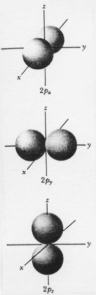
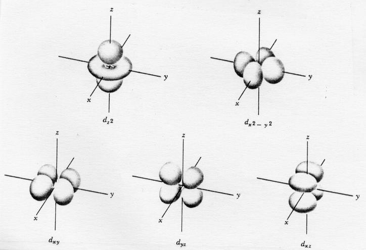
2 Atomic Orbitals s-orbitals p-orbitals d-orbitals
3 Chemical Bonding * s,p,d,etc. E B s,p,d,etc. Overlap of half-filled orbitals - bond formation H A H B H A - H B = H 2 Formation of Molecular Hydrogen from Atoms * s,p,d,etc. E B s,p,d,etc. Overlap of filled orbitals - no bonding

4 Periodic Chart

 Valence Band Si crystal E V Silicon")
5 Crystal Bonding sp 3 antibonding orbitals sp 3 bonding orbitals Conduction Band E C 3p 3s sp 3 E g Si (separated atoms) Si (atoms interact to form tetrahedral bonding geometry) Valence Band Si crystal E V Silicon Crystal Bonding
6 Semiconductor Band Structures Silicon Germanium Gallium Arsenide
7 Intrinsic Semiconductor E C N C Conduction Band E F E g E V N V Valence Band Aggregate Band Structure Fermi-Dirac Distribution
8 n-type Semiconductor E C N C Conduction Band Shallow Donor States E F E i E g E V N V Valence Band Aggregate Band Structure Donor Ionization Fermi-Dirac Distribution
9 p-type Semiconductor E C N C Conduction Band E i E F E V N V Shallow Acceptor States Valence Band E g Aggregate Band Structure Acceptor Ionization Fermi-Dirac Distribution
10 Temperature Dependence Fermi level shift in extrinsic silicon Mobile electron concentration (N D = 1.15(10 16 ) cm 3 )
11 Carrier Mobility No Field Field Present Pictorial representation of carrier trajectory Carrier drift velocity vs applied field in intrinsic silicon
12 Effect of Dopant Impurities Effect of total dopant concentration on carrier mobility Resistivity of bulk silicon as a function of net dopant concentration
13 The Seven Crystal Systems
14 Bravais Lattices
15 Diamond Cubic Lattice a = lattice parameter; length of cubic unit cell edge Silicon atoms have tetrahedral coordination in a FCC (face centered cubic) Bravais lattice
16 Miller Indices z O y z x 100 O y 110 x z O y x 111


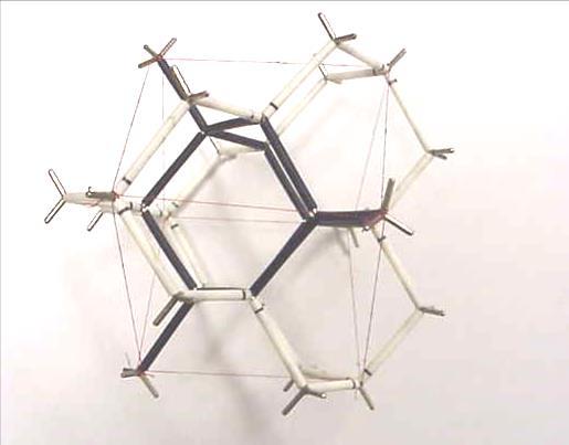
17 Diamond Cubic Model
18 Cleavage Planes Crystals naturally have cleavage planes along which they are easily broken. These correspond to crystal planes of low bond density Bonds per unit cell Plane area per cell a 2 2 a 2 2 a Bond Density a a a a a In the diamond cubic structure, cleavage occurs along 110 planes.
![[100]](/docs-images/78/77410802/images/19-0.jpg)
19 [100] Orientation
![[110]](/docs-images/78/77410802/images/20-0.jpg)
20 [110] Orientation
![[111]](/docs-images/78/77410802/images/21-0.jpg)
21 [111] Orientation
![[100]](/docs-images/78/77410802/images/22-0.jpg "Cleavage")
22 [100] Cleavage
![[111]](/docs-images/78/77410802/images/23-0.jpg "Cleavage")
23 [111] Cleavage
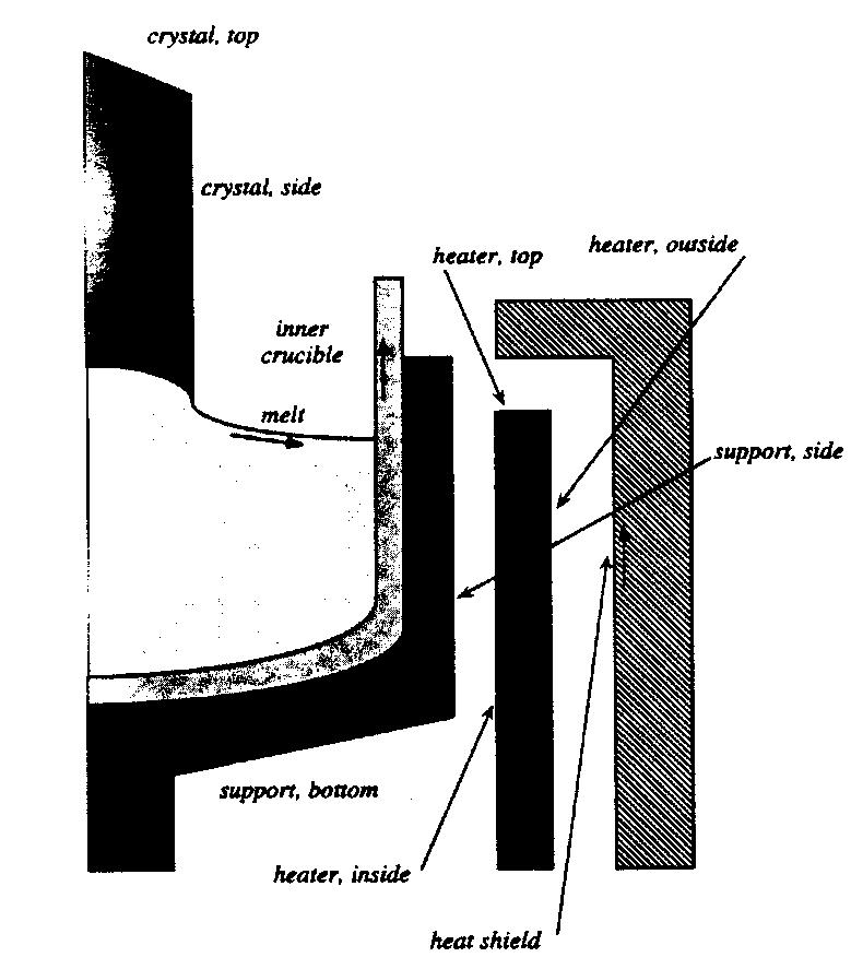
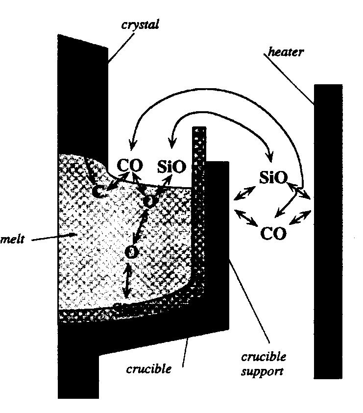
24 Czochralski Process
 dia.")
25 Seed Rod (Single Crystal Si) dia. = ~1 cm

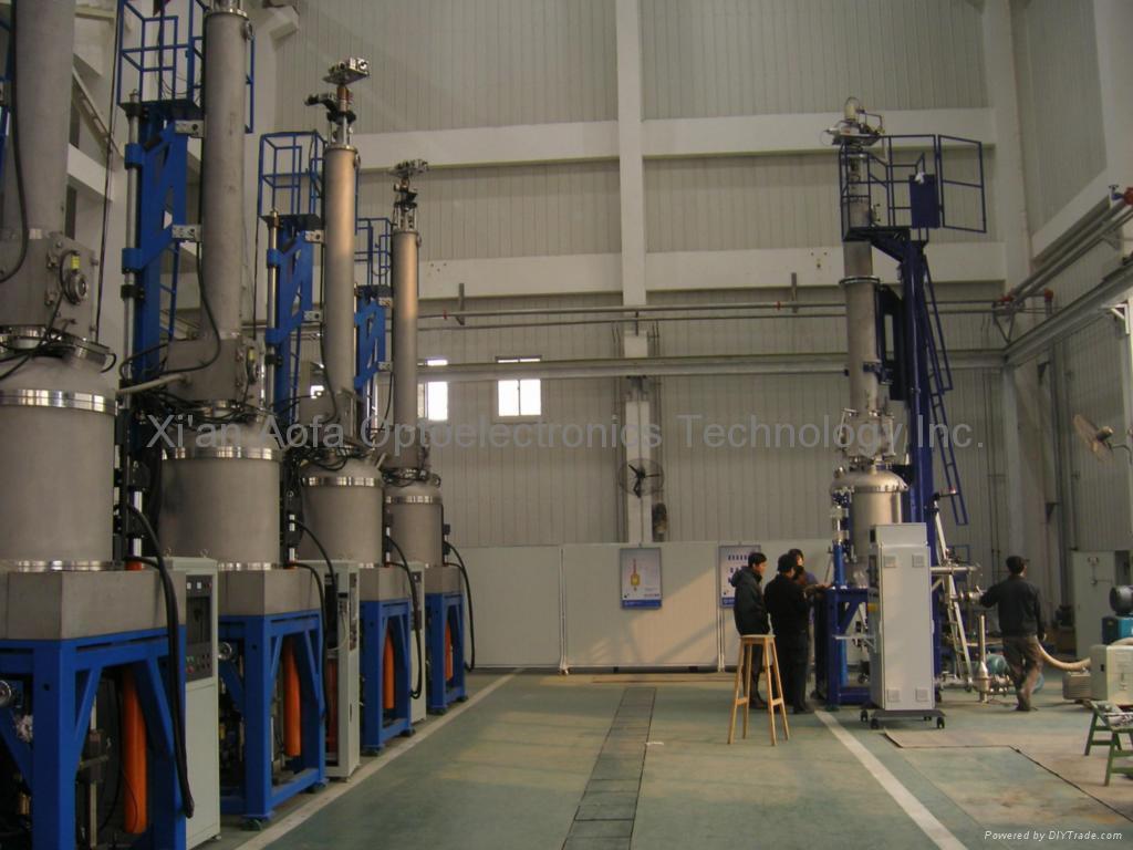
26 Czochralski Process Equipment Image courtesy Microchemicals
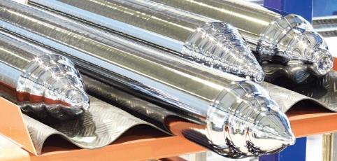
27 Czochralski Factory and Boules
28 D opant Conce ntration R atio CZ Growth under Rapid Stirring C s C l x=0 dx Distribution Coefficients Dopant K B 0.72 P 0.32 As 0.27 Sb Ga Al In Le ngth Fractio n CZ Dopant Profiles under Conditions of Rapid Stirring
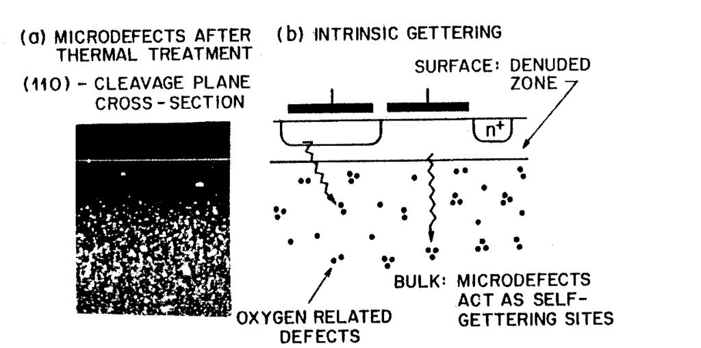
29 Enrichment at the Melt Interface

30 Zone Refining Si Ingot Heater Ingot slowly passes through the needle s eye heater so that the molten zone is swept through the ingot from one end to the other
31 Dopant Concentration Ratio Single Pass FZ Process L C s C o x=0 dx x Zone Lengths
32 Dopant Concentration Ratio Multiple Pass FZ Process Zone Lengths Almost arbitrarily pure silicon can be obtained by multiple pass zone refining.
33 Vacancy (Schottky Defect) Dangling Bonds
34 Self-Interstital
35 Dislocations Edge Dislocation Screw Dislocation

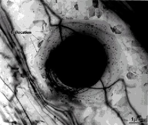
36 Burgers Vector Edge Dislocation Screw Dislocation Dislocations in Silicon [100] [111]
37 Stacking Faults Intrinsic Stacking Fault Extrinsic Stacking Fault
38 Vacancy-Interstitial Equilibrium Formation of a Frenkel defect - vacancy-interstitial pair L V + I Chemical Equilibrium K eq = [ V ][ I]
39 Thermodynamic Potentials E = Internal Energy H = Enthalpy (heat content) A = Helmholtz Free Energy G = Gibbs Free Energy For condensed phases: E and H are equivalent = internal energy (total system energy) A and G are equivalent = free energy (energy available for work) A = E TS T = Absolute Temperature S = Entropy (disorder) S = k ln W Boltzmann s relation
40 Vacancy Formation A = ME TS Mv v Mv S Mv = E v S W Mv k Mv = ln W = = ~ 2.3eV k ln W Mv N! ( N M)! M! N! = k ln ( N M )! M! Mv A Mv = ME v NkT ln N + MkT ln M + ( N M) ktln( N M)
41 Additional Vacancy Formation M A = E + kt ln M kt ln( N M) Mv v M = N exp E kt v Vacancy concentration
42 Equilibrium Constant Interstitial concentration N N 8 5 = = = kt E N kt E N M i i exp 8 5 exp + = kt E E N K i v eq exp 8 5 2
43 Internal Gettering Gettering removes harmful impurities from the front side of the wafer rendering them electrically innocuous. O 2 O 2 O 2 O 2 O 2 denuded zone O O O O O O O O O O O O High temperature anneal - denuded zone formation oxygen nuclei Low temperature anneal - nucleation oxide precipitates (with dislocations and stacking faults) Intermediate temperature anneal - precipitate growth
44 Oxygen Solubility in Silicon 1.0E+19 Interstitial Oxygen Concentration, per cm 3 1.0E E Temperature, deg C
45 Oxygen Outdiffusion
46 Precipitate Free Energy 3 4r A = ne nts + g SiO + 4 r 2 SiO 2 3 r A = ne nts + g+ 8r 2 4r SiO 2 SiO2 a) - Free energy of formation of a spherical precipitate as a function of radius b) - Saturated solid solution of B (e.g., interstitial oxygen) in A (e.g., silicon crystal) c) - Nucleus formation 2
47 Critical Radius r 2 = crit ne nts + SiO 2 SiO 2 g a) If critical radius exists, then a larger precipitate grows large b) If critical radius exists, then a smaller percipitate redissolves

48 Substrate Characterization by XRD q q Constructive Interference Destructive Interference Bragg pattern - [hk0], [h0l], or [0kl]

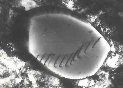
49 Wafer Finishing Ingot slicing into raw wafers Spindle Carrier Pad Capture Ring Table Wafer Insert Schematic of chemical mechanical polishing
")
50 Vapor-Liquid-Solid (VLS) Growth H 2 H 2 H 2 H 2 catalyst SiH 4 SiH 4 substrate substrate substrate Si nanowires grown by VLS (at IBM)
51 Gold-Silicon Eutectic liquid A B solid A eutectic melt mixed with solid gold B eutectic melt mixed with solid silicon

52 Silicon Dioxide Network Non-bridging oxygen SiO 4 tetrahedron Silanol
53 Thermal Oxidation C C S C G C o F 1 C i F 2 F 3 Si Substrate x Thermal SiO 2 Film Gas One dimensional model of oxide growth Deal-Grove growth kinetics
54 Steady-state Fluxes F = h ( C C 1 G G S Mass transport flux ) D F = ( C C 2 o i x Diffusion flux ) F 3 =k s C i Reaction flux 1) Diffusion flux is in-diffusion. Any products, e.g., H 2, must out-diffuse. However, out-diffusion is fast and generally not limiting. 2) Mass transport is generally never limiting.
55 Henry's Law H = C C o S Distribution equilibrium (Henry's Law) Reaction = Mass Transport k s C i = h G C G C o H k C C = s i + G h G C o H
56 Steady-state Concentrations Reaction = Diffusion ) ( i o i s C C x D C k = Gas phase concentration related to reaction concentration i s o C D x k C + = 1 i s G s G C HD x k H h k C + + = 1
57 Deal-Grove Model Relationship between thickness and time: = G s G G s h H k t t ND HC h H k D x 1 ) ( What if an oxide of thickenss, x 0, is already on the wafer? Must calculate equivalent growth time under desired conditions = = D x k h Hk HC k dt dx N F s G s G s + + = x h H k D x DHC N t G s G
58 Deal-Grove Rate Constants B/A => Linear Rate Constant B => Parabolic Rate Constant + = s h G H k D A 1 2 N DHC B G 2 = + = G s G h Hk N C A B 1 1
59 Oxidation Kinetics Energy Transition E a Reactant Product E Process Coordinate Rate constants for wet and dry oxidation on [100] and [111] surfaces Process B/A for [100] B/A for [111] B Dry Oxidation 1.03(10 3 kt ) (10 3 kt ) 2. kt e 00 e 00 e 23 Steam Oxidation 2.70(10 4 kt ) (10 4 kt ) 2. kt e 05 e 05 e 79 Note: Activation energies are in ev s, B/A is in m/sec, B is in m 2 /sec
60 Linear Rate Constant Orientation dependence for [100] and [111] surfaces affects only the pre-exponential factor and not the activation energy
61 Parabolic Rate Constant No orientation dependence since the parabolic rate constant describes a diffusion limited process
62 Pressure Dependence Oxidation rates scale linearly with oxidant pressure or partial pressure
63 Rapid Initial Oxidation in Pure O 2 This data taken at 700C in dry oxygen to investigate initial rapid oxide growth
64 Metal-Metal Contact E vac f 1 f 2 y = f 2 f 1 E F1 E F2 E F + + Metal 1 Metal 2
65 Metal-Silicon Contact E vac f M f Si f Si f M E FM E c E FSi E F + + E v Metal Silicon
66 Effect of a Metal Contact on Silicon E c E c E i j F j F E F + + Depletion (p-type) E v E F + + Inversion (p-type) E i E v E c E c E F + + j F E i E v E F j F E i E v Accumulation (n-type) Flat Band (n-type) + + E c E F j F E i E v Depletion (n-type)
67 Metal-Oxide-Silicon Capacitor E vac f Si f M f M f Si f SiO2 E FSi E F + E FM E C E V Metal Silicon Dioxide Silicon
68 MOS Capacitor on Doped Silicon E C E C E FM j F E i E FSi E FM + E V E V Depletion (p-type) Accumulation (n-type) + j F E FSi E i V g 0 v Schematic of biased MOS capacitor
69 Biased MOS Capacitors E FM E FM E C E C j F E FSi j F E i E FSi E i Accumulation (p-type) E V Inversion (n-type) E V E C E FM E C E FM j F E i E FSi E V j F E FSi E i Depletion (p-type) Depletion (n-type) E V E C j F E i E FSi E V E C E FSi E FM j F Ei E FM E V Inversion (p-type) Accumulation (n-type)
70 Capacitance Capacitance CV Response quasistatic 6 5 n-type substrate 4 3 high frequency Bias Voltage depletion approximation quasistatic 6 5 p-type substrate depletion approximation high frequency Bias Voltage
71 Surface Charge Density Surface Charge Density Surface Charge Density inversion depletion n type substrate 10 accumulation Bias Voltage blue: positive surface charge red: negative surface charge inversion depletion p type substrate 10 accumulation Bias Voltage
72 Capacitance, Charge, and Potential 2 d j ( x) = 2 dx Poisson s equation (1-D) s ( x) = q p( x) n( x) + N D N A Charge density for a uniformly doped substrate i = skt 2 2q n Intrinsic Debye Length: a measure of how much an external electric field penetrates pure silicon i
73 The Depletion Approximation ) ( ) ( 2 2 x N x N q dx d A D s = j Carrier concentrations are negligible in the depletion region = i D A D A s d n N N N N q kt x ln 4 2 max Maximum depletion width D A s D N N q kt = 2 Extrinsic Debye Length: a measure of how much an external electric field penetrates doped silicon
74 CV vs Doping and Oxide Thickness 10 Capacitance (dimensionless linear scale) Substrate Doping p-type substrate Capacitance (dimensionless logarithmic scale) Bias Voltage (dimensionless linear scale) Oxide Thickness
75 CV Measurements C Quasi-static CV C High Frequency CV C ox C ox C min C min V V C C ox Deep Depletion Effect C min slow sweep fast very fast extremely fast V C Flat Band Shift C Fast Interface States C ox Ideal C ox Ideal C FB C FB Actual Actual C min C min V FB V FB V V FB V
76 Interface States E C E F j F E i E V Interface states caused by broken symmetry at interface E C j F E i E FSi E FM E V Interface states p-type depletion E FM j F E C E FSi E i E V Interface states n-type depletion
77 Interface State Density Interface state density is always higher on [111] than [100]
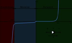
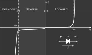
78 IV Response avalanche breakdown log J Fowler-Nordheim tunneling Very T hin T hin T hick 10 MV/cm E Logarithm of current density (J) vs applied electric field (E)
79 Conduction Mechanisms J = 2 E AFN E exp E o Fowler-Nordheim tunneling J J J J qe = AFP E exp qfb kt ox Frenkel-Poole emission qe = A* T 2 exp qfb kt 4 ox Schottky emission = A E exp e q E ae kt Ohmic (electronic) conduction Ai E = exp q Eai kt Ionic conduction T J = 9 8x ox ox e 3 o V 2 Mobility limited breakdown current
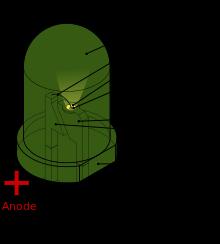
80 Oxide Reliability 100% Per cent Failed poor reliability good reliability 0% infant mortality time, t, or total charge, Q Each point represents a failed MOS structure - stress is continued until all devices fail QBD - charge to breakdown - constant current stress TDBD - time dependent breakdown - constant voltage stress
81 Linear Transport Processes Ohm s Law of electrical conduction: j = E = E/ J = electric current density, j (units: A/cm 2 ) J = LX J = Flux, X = Force, L = Transport Coefficient X = electric field, E = V (units: volt/cm) V = electrical potential Fourier s Law of heat transport: q = T L = conductivity, = 1/ (units: mho/cm) = resistivity ( cm) J = heat flux, q (units: W/cm 2 ) X = thermal force, T (units: K/cm) T = temperature Fick s Law of diffusion: F = DC L = thermal conductivity, (units: W/K cm) J = material flux, F (units: /sec cm 2 ) X = diffusion force, C (units: /cm 4 ) C = concentration Newton s Law of viscous fluid flow: F u = u L = diffusivity, D (units: cm 2 /sec) J = velocity flux, F u (units: /sec 2 cm) X = viscous force, u (units: /sec) u = fluid velocity L = viscosity, (units: /sec cm)
82 Diffusion x A F(x) x F(x ) + Diffusion in a rectangular bar of constant cross section x C t = D 2 C 2 x Fick s Second Law 2 xx0 4Dt C x, t = e 2 N Dt Instantaneous Source - Gaussian profile C N 2 x x 2 Dt 0 0 x, t = erfc Constant Source - error function profile
83 Instantaneous Source Profile Linear scale Log scale
84 Constant Source Profile Linear scale Log scale
85 Surface Probing r r I x f Substrate I T hin Film Substrate Single probe injecting current into a bulk substrate Single probe injecting current into a conductive thin film I I s s s Substrate Four point probe
86 pn Junction E vac E c E Fn E i E F E Fp E v n type Silicon p type Silicon
87 Junction Depth x J red: background doping black: diffused doping x J
88 Unbiased pn Junctions Band Diagram E F Charge Density E Electric Field V Potential
89 Biased pn Junctions I IV Characteristics I 0 V 1 C 2 CV Characteristics V pn V
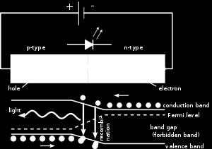
90 Photovoltaic Effect V OC V I SC I


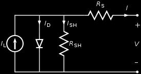
91 Solar Cell typical cross section equivalent circuit
92 Solar Cell IV Curve I I SC I max P V max V OC
93 Effect of Parasitics, Temperature, etc. effect of R S effect of R SH effect of I 0 effect of n effect of T


94 Solar Cell Technology Commercial solar cell
95 LED IV Characteristics
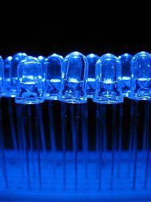
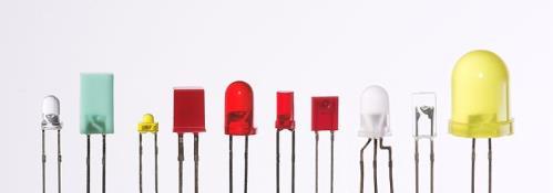
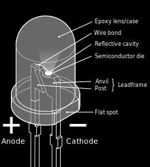
96 LED Technology Commercial LED s RGB spectrum white spectrum (with phosphor)
97 Diffusion Mechanisms Vacancy Diffusion - Substitutional impurities, e.g., shallow level dopants (B, P, As, Sb, etc.), Diffusivity is relatively small for vacancy diffusion. Interstitial Diffusion - Interstitial impurities, e.g., small atoms and metals (O, Fe, Cu, etc.), Diffusivity is much larger, hence interstitial diffusion is fast compared to vacancy diffusion. Interstitialcy Mechanism - Enhances the diffusivity of substitutional impurities due to exchange with silicon self-interstitials. This leads to enhanced diffusion in the vicinity of the substrate surface during thermal oxidation (socalled oxidation enhanced diffusion ).
98 Defect-Carrier Equilibria x + V V + h K = V V V x p = + = V V + h K V = V V = p x + + V V + e K = V V V + x n V V + e K V = V V ++ + n Vacancies interact with mobile carriers and become charged. In this case, the concentrations are governed by classical mass action equilibria.
99 Arrhenius Constants for Dopant Atoms Atomic Species I Diffusion Mechanism r V r D oi (cm 2 /sec) r Q I (ev) Si V V V V x = As V x V B V V x Ga V V x P V V V x = Sb V V x N x V
100 Arrhenius Constants for Other Species Atomic Species Mechanism, Temperature, etc. D oi (cm 2 /sec) Q I (ev) Ge substitutional 6.25(10 5 ) 5.28 Cu ( C) ( C) 4.7( ) Ag 3 2(10 ) 1.6 Au substitutional interstitial ( C) 2.8(10 2.4(10 1.1( ) ) ) Pt Fe 3 6.2(10 ) 0.87 Co 9.2(10 4 ) 2.8 C S O H (10 ) 0.48 He
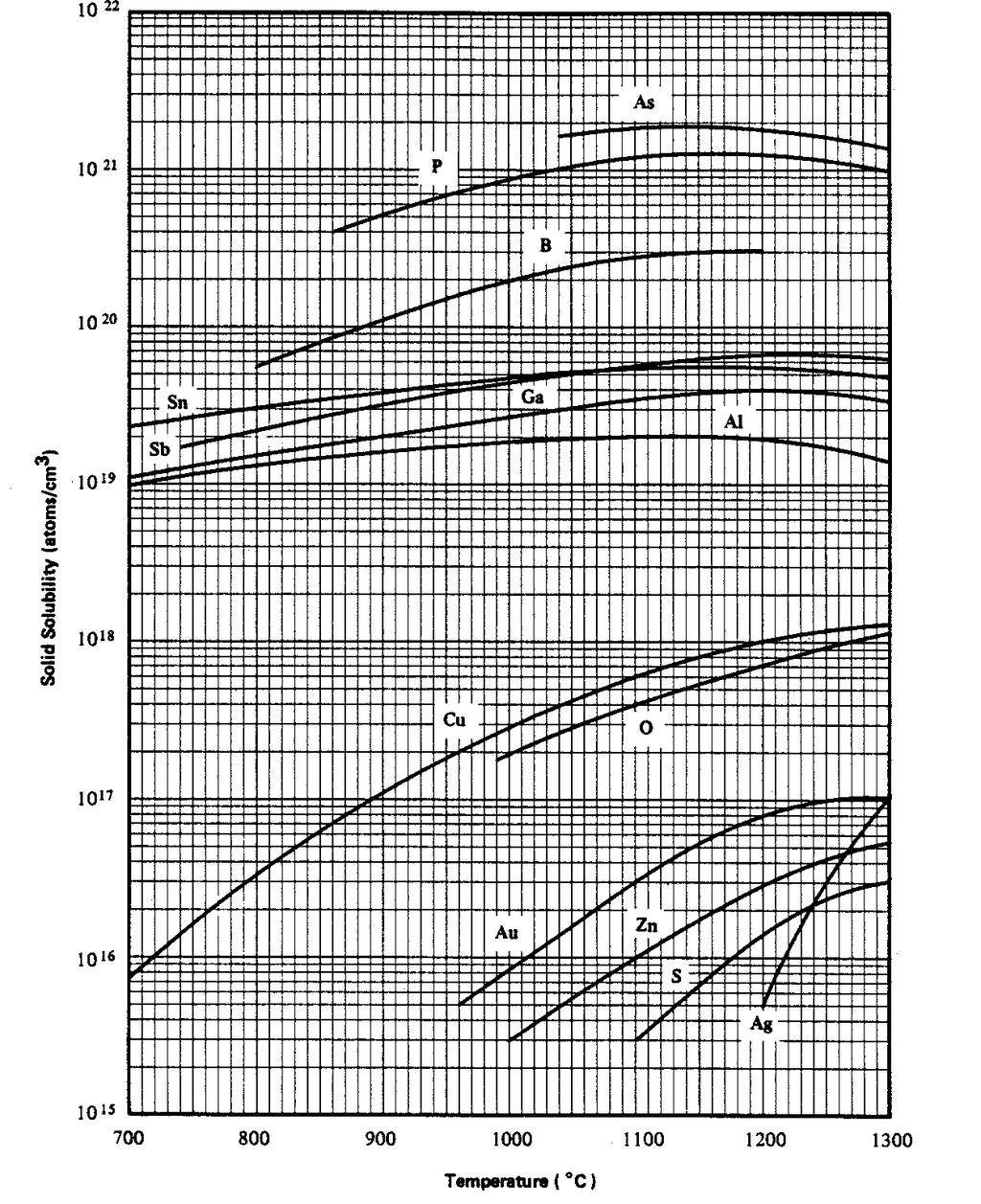
101 Solid Solubilities
102 Ion Implantation Dopant species are ionized and accelerated by a very high electric field. The ions then strike the substrate at energies from 10 to 500 kev and penetrate a short distance below the surface. kˆ q vi tangent plane (edge on) v i q i vˆ ^ b c ˆv s vs Elementary hard sphere collision
103 Co-linear or Centered Collision b=0 c= q=0 tangent plane (edge on) vˆ ^ ˆv v i vi kˆ i s vs mi ms v i = vi mi + ms ; v s 2mi = vi mi + ms Clearly, if m i <m s, then v i is negative. This means that light implanted ions tend to be scattered back toward the surface. Conversely, if m i >m s, then v i is positive and heavy ions tend to be scattered forward into the bulk. Obviously, if m i equals m s, then v i ˆv 0 vanishes. In any case, recoiling silicon atoms are scattered deeper into the substrate.
104 Stopping Mechanisms Nuclear Stopping - Direct interaction between atomic nuclei; resembles an elementary two body collision and causes most implant damage. Electronic Stopping - Interaction between atomic electron clouds; sort of a viscous drag as in a liquid medium. Causes little damage.
105 Implant Range Range - Total distance traversed by an ion implanted into the substrate. Projected Range - Average penetration depth of an implanted ion.
106 Implant Straggle Projected Straggle - Variation in penetration depth. (Corresponds to standard deviation if the implanted profile is Gaussian.)
107 Channeling Channeling is due to the crystal structure of the substrate.
108 Implantation Process For a light dose, damage is isolated. As dose is increased, damage sites become more dense and eventually merge to form an amorphous layer. For high dose implants, the amorphous region can reach all the way to the substrate surface.
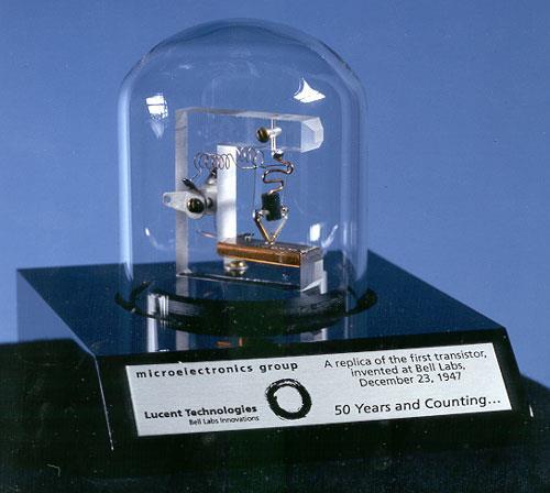
109 Point-Contact Transistor
110 Bipolar Junction Transistor E B C n p n
111 Junction FET S G D n p n
112 MOSFET S G D n n p enhancement mode S G D n n p depletion mode
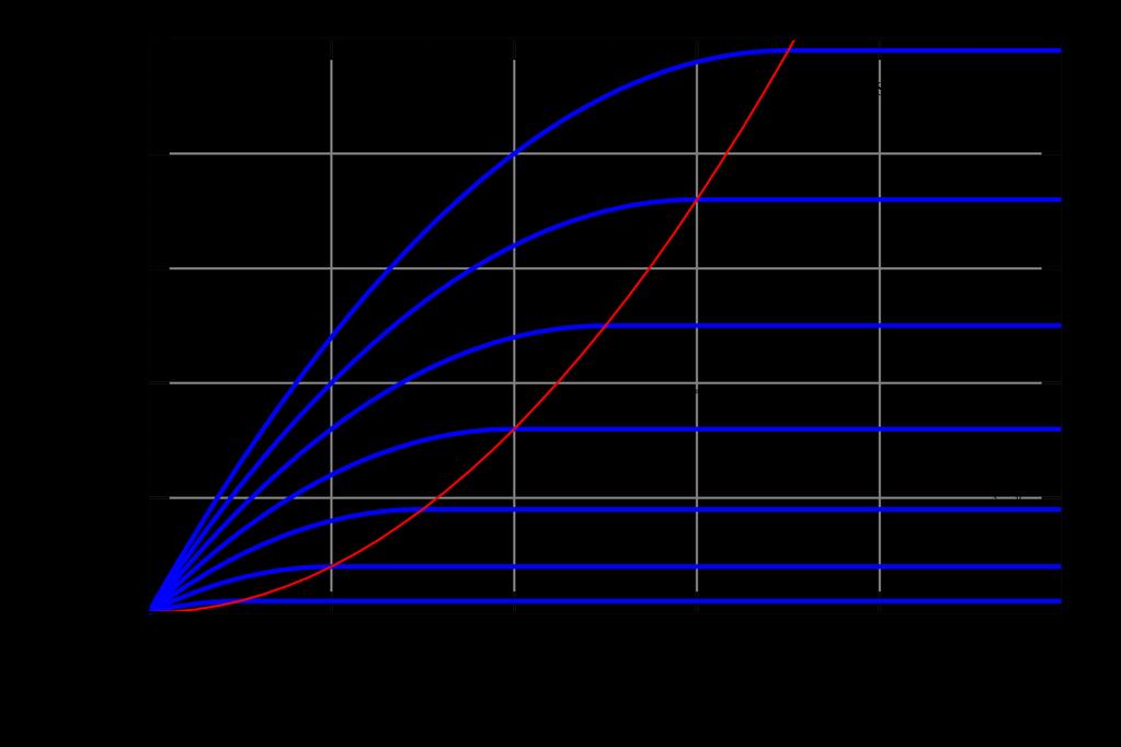
113 Enhancement Mode FET 7 V 6 V 5 V 4 V
1 Name: Student number: DEPARTMENT OF PHYSICS AND PHYSICAL OCEANOGRAPHY MEMORIAL UNIVERSITY OF NEWFOUNDLAND. Fall :00-11:00
 1 Name: DEPARTMENT OF PHYSICS AND PHYSICAL OCEANOGRAPHY MEMORIAL UNIVERSITY OF NEWFOUNDLAND Final Exam Physics 3000 December 11, 2012 Fall 2012 9:00-11:00 INSTRUCTIONS: 1. Answer all seven (7) questions.
Review Energy Bands Carrier Density & Mobility Carrier Transport Generation and Recombination
 Review Energy Bands Carrier Density & Mobility Carrier Transport Generation and Recombination The Metal-Semiconductor Junction: Review Energy band diagram of the metal and the semiconductor before (a)
Appendix 1: List of symbols
 Appendix 1: List of symbols Symbol Description MKS Units a Acceleration m/s 2 a 0 Bohr radius m A Area m 2 A* Richardson constant m/s A C Collector area m 2 A E Emitter area m 2 b Bimolecular recombination
Ion Implantation ECE723
 Ion Implantation Topic covered: Process and Advantages of Ion Implantation Ion Distribution and Removal of Lattice Damage Simulation of Ion Implantation Range of Implanted Ions Ion Implantation is the
Section 7: Diffusion. Jaeger Chapter 4. EE143 Ali Javey
 Section 7: Diffusion Jaeger Chapter 4 Surface Diffusion: Dopant Sources (a) Gas Source: AsH 3, PH 3, B 2 H 6 (b) Solid Source BN Si BN Si (c) Spin-on-glass SiO 2 +dopant oxide (d) Liquid Source. Fick s
Xing Sheng, 微纳光电子材料与器件工艺原理. Doping 掺杂. Xing Sheng 盛兴. Department of Electronic Engineering Tsinghua University
 微纳光电子材料与器件工艺原理 Doping 掺杂 Xing Sheng 盛兴 Department of Electronic Engineering Tsinghua University xingsheng@tsinghua.edu.cn 1 Semiconductor PN Junctions Xing Sheng, EE@Tsinghua LEDs lasers detectors solar
Semiconductor Physics fall 2012 problems
 Semiconductor Physics fall 2012 problems 1. An n-type sample of silicon has a uniform density N D = 10 16 atoms cm -3 of arsenic, and a p-type silicon sample has N A = 10 15 atoms cm -3 of boron. For each
Section 12: Intro to Devices
 Section 12: Intro to Devices Extensive reading materials on reserve, including Robert F. Pierret, Semiconductor Device Fundamentals Bond Model of Electrons and Holes Si Si Si Si Si Si Si Si Si Silicon
Section 12: Intro to Devices
 Section 12: Intro to Devices Extensive reading materials on reserve, including Robert F. Pierret, Semiconductor Device Fundamentals EE143 Ali Javey Bond Model of Electrons and Holes Si Si Si Si Si Si Si
Semiconductor Physical Electronics
 Semiconductor Physical Electronics Sheng S. Li Department of Electrical Engineering University of Florida Gainesville, Florida Plenum Press New York and London Contents CHAPTER 1. Classification of Solids
Fabrication Technology, Part I
 EEL5225: Principles of MEMS Transducers (Fall 2004) Fabrication Technology, Part I Agenda: Microfabrication Overview Basic semiconductor devices Materials Key processes Oxidation Thin-film Deposition Reading:
A semiconductor is an almost insulating material, in which by contamination (doping) positive or negative charge carriers can be introduced.
 positive or negative charge carriers can be introduced.") Semiconductor A semiconductor is an almost insulating material, in which by contamination (doping) positive or negative charge carriers can be introduced. Page 2 Semiconductor materials Page 3 Energy levels
Semiconductor A semiconductor is an almost insulating material, in which by contamination (doping) positive or negative charge carriers can be introduced. Page 2 Semiconductor materials Page 3 Energy levels
September 21, 2005, Wednesday
 , Wednesday Doping and diffusion I Faster MOSFET requires shorter channel P + Poly Al Al Motivation Requires shallower source, drain Al P + Poly Al source drain Shorter channel length; yes, but same source
Consider a uniformly doped PN junction, in which one region of the semiconductor is uniformly doped with acceptor atoms and the adjacent region is
 CHAPTER 7 The PN Junction Consider a uniformly doped PN junction, in which one region of the semiconductor is uniformly doped with acceptor atoms and the adjacent region is uniformly doped with donor atoms.
Chapter 7. The pn Junction
 Chapter 7 The pn Junction Chapter 7 PN Junction PN junction can be fabricated by implanting or diffusing donors into a P-type substrate such that a layer of semiconductor is converted into N type. Converting
MOS CAPACITOR AND MOSFET
 EE336 Semiconductor Devices 1 MOS CAPACITOR AND MOSFET Dr. Mohammed M. Farag Ideal MOS Capacitor Semiconductor Devices Physics and Technology Chapter 5 EE336 Semiconductor Devices 2 MOS Capacitor Structure
Electronic Devices & Circuits
 Electronic Devices & Circuits For Electronics & Communication Engineering By www.thegateacademy.com Syllabus Syllabus for Electronic Devices Energy Bands in Intrinsic and Extrinsic Silicon, Carrier Transport,
Schottky Rectifiers Zheng Yang (ERF 3017,
 ECE442 Power Semiconductor Devices and Integrated Circuits Schottky Rectifiers Zheng Yang (ERF 3017, email: yangzhen@uic.edu) Power Schottky Rectifier Structure 2 Metal-Semiconductor Contact The work function
Review of Semiconductor Fundamentals
 ECE 541/ME 541 Microelectronic Fabrication Techniques Review of Semiconductor Fundamentals Zheng Yang (ERF 3017, email: yangzhen@uic.edu) Page 1 Semiconductor A semiconductor is an almost insulating material,
DIFFUSION - Chapter 7
 DIFFUSION - Chapter 7 Doping profiles determine many short-channel characteristics in MOS devices. Resistance impacts drive current. Scaling implies all lateral and vertical dimensions scale by the same
EECS130 Integrated Circuit Devices
 EECS130 Integrated Circuit Devices Professor Ali Javey 10/02/2007 MS Junctions, Lecture 2 MOS Cap, Lecture 1 Reading: finish chapter14, start chapter16 Announcements Professor Javey will hold his OH at
collisions of electrons. In semiconductor, in certain temperature ranges the conductivity increases rapidly by increasing temperature
 1.9. Temperature Dependence of Semiconductor Conductivity Such dependence is one most important in semiconductor. In metals, Conductivity decreases by increasing temperature due to greater frequency of
Final Examination EE 130 December 16, 1997 Time allotted: 180 minutes
 Final Examination EE 130 December 16, 1997 Time allotted: 180 minutes Problem 1: Semiconductor Fundamentals [30 points] A uniformly doped silicon sample of length 100µm and cross-sectional area 100µm 2
ESE 372 / Spring 2013 / Lecture 5 Metal Oxide Semiconductor Field Effect Transistor
 Metal Oxide Semiconductor Field Effect Transistor V G V G 1 Metal Oxide Semiconductor Field Effect Transistor We will need to understand how this current flows through Si What is electric current? 2 Back
an introduction to Semiconductor Devices
 an introduction to Semiconductor Devices Donald A. Neamen Chapter 6 Fundamentals of the Metal-Oxide-Semiconductor Field-Effect Transistor Introduction: Chapter 6 1. MOSFET Structure 2. MOS Capacitor -
Semiconductor Physics Problems 2015
 Semiconductor Physics Problems 2015 Page and figure numbers refer to Semiconductor Devices Physics and Technology, 3rd edition, by SM Sze and M-K Lee 1. The purest semiconductor crystals it is possible
Quiz #1 Practice Problem Set
 Name: Student Number: ELEC 3908 Physical Electronics Quiz #1 Practice Problem Set? Minutes January 22, 2016 - No aids except a non-programmable calculator - All questions must be answered - All questions
Semiconductor Junctions
 8 Semiconductor Junctions Almost all solar cells contain junctions between different materials of different doping. Since these junctions are crucial to the operation of the solar cell, we will discuss
Metal Semiconductor Contacts
 Metal Semiconductor Contacts The investigation of rectification in metal-semiconductor contacts was first described by Braun [33-35], who discovered in 1874 the asymmetric nature of electrical conduction
Semiconductor Physics fall 2012 problems
 Semiconductor Physics fall 2012 problems 1. An n-type sample of silicon has a uniform density N D = 10 16 atoms cm -3 of arsenic, and a p-type silicon sample has N A = 10 15 atoms cm -3 of boron. For each
Fabrication and Characterization of Al/Al2O3/p-Si MOS Capacitors
 Fabrication and Characterization of Al/Al2O3/p-Si MOS Capacitors 6 MOS capacitors were fabricated on silicon substrates. ALD deposited Aluminum Oxide was used as dielectric material. Various electrical
Chapter 4: Bonding in Solids and Electronic Properties. Free electron theory
 Chapter 4: Bonding in Solids and Electronic Properties Free electron theory Consider free electrons in a metal an electron gas. regards a metal as a box in which electrons are free to move. assumes nuclei
ESE 570: Digital Integrated Circuits and VLSI Fundamentals
 ESE 570: Digital Integrated Circuits and VLSI Fundamentals Lec 4: January 23, 2018 MOS Transistor Theory, MOS Model Penn ESE 570 Spring 2018 Khanna Lecture Outline! CMOS Process Enhancements! Semiconductor
Ion Implantation. alternative to diffusion for the introduction of dopants essentially a physical process, rather than chemical advantages:
 Ion Implantation alternative to diffusion for the introduction of dopants essentially a physical process, rather than chemical advantages: mass separation allows wide varies of dopants dose control: diffusion
ESE 570: Digital Integrated Circuits and VLSI Fundamentals
 ESE 570: Digital Integrated Circuits and VLSI Fundamentals Lec 4: January 29, 2019 MOS Transistor Theory, MOS Model Penn ESE 570 Spring 2019 Khanna Lecture Outline! CMOS Process Enhancements! Semiconductor
MSE 310/ECE 340: Electrical Properties of Materials Fall 2014 Department of Materials Science and Engineering Boise State University
 MSE 310/ECE 340: Electrical Properties of Materials Fall 2014 Department of Materials Science and Engineering Boise State University Practice Final Exam 1 Read the questions carefully Label all figures
Sheng S. Li. Semiconductor Physical Electronics. Second Edition. With 230 Figures. 4) Springer
 Springer") Sheng S. Li Semiconductor Physical Electronics Second Edition With 230 Figures 4) Springer Contents Preface 1. Classification of Solids and Crystal Structure 1 1.1 Introduction 1 1.2 The Bravais Lattice
Sheng S. Li Semiconductor Physical Electronics Second Edition With 230 Figures 4) Springer Contents Preface 1. Classification of Solids and Crystal Structure 1 1.1 Introduction 1 1.2 The Bravais Lattice
KATIHAL FİZİĞİ MNT-510
 KATIHAL FİZİĞİ MNT-510 YARIİLETKENLER Kaynaklar: Katıhal Fiziği, Prof. Dr. Mustafa Dikici, Seçkin Yayıncılık Katıhal Fiziği, Şakir Aydoğan, Nobel Yayıncılık, Physics for Computer Science Students: With
Electronics The basics of semiconductor physics
 Electronics The basics of semiconductor physics Prof. Márta Rencz, Gergely Nagy BME DED September 16, 2013 The basic properties of semiconductors Semiconductors conductance is between that of conductors
Ion Implant Part 1. Saroj Kumar Patra, TFE4180 Semiconductor Manufacturing Technology. Norwegian University of Science and Technology ( NTNU )
") 1 Ion Implant Part 1 Chapter 17: Semiconductor Manufacturing Technology by M. Quirk & J. Serda Spring Semester 2014 Saroj Kumar Patra,, Norwegian University of Science and Technology ( NTNU ) 2 Objectives
1 Ion Implant Part 1 Chapter 17: Semiconductor Manufacturing Technology by M. Quirk & J. Serda Spring Semester 2014 Saroj Kumar Patra,, Norwegian University of Science and Technology ( NTNU ) 2 Objectives
ECE 340 Lecture 39 : MOS Capacitor II
 ECE 340 Lecture 39 : MOS Capacitor II Class Outline: Effects of Real Surfaces Threshold Voltage MOS Capacitance-Voltage Analysis Things you should know when you leave Key Questions What are the effects
Unit IV Semiconductors Engineering Physics
 Introduction A semiconductor is a material that has a resistivity lies between that of a conductor and an insulator. The conductivity of a semiconductor material can be varied under an external electrical
Lecture 04 Review of MOSFET
 ECE 541/ME 541 Microelectronic Fabrication Techniques Lecture 04 Review of MOSFET Zheng Yang (ERF 3017, email: yangzhen@uic.edu) What is a Transistor? A Switch! An MOS Transistor V GS V T V GS S Ron D
Introduction to Semiconductor Physics. Prof.P. Ravindran, Department of Physics, Central University of Tamil Nadu, India
 Introduction to Semiconductor Physics 1 Prof.P. Ravindran, Department of Physics, Central University of Tamil Nadu, India http://folk.uio.no/ravi/cmp2013 Review of Semiconductor Physics Semiconductor fundamentals
Thermal Oxidation of Si
 Thermal Oxidation of General Properties of O 2 Applications of thermal O 2 Deal-Grove Model of Oxidation Thermal O 2 is amorphous. Weight Density = 2.20 gm/cm 3 Molecular Density = 2.3E22 molecules/cm
Classification of Solids
 Classification of Solids Classification by conductivity, which is related to the band structure: (Filled bands are shown dark; D(E) = Density of states) Class Electron Density Density of States D(E) Examples
R. Ludwig and G. Bogdanov RF Circuit Design: Theory and Applications 2 nd edition. Figures for Chapter 6
 R. Ludwig and G. Bogdanov RF Circuit Design: Theory and Applications 2 nd edition Figures for Chapter 6 Free electron Conduction band Hole W g W C Forbidden Band or Bandgap W V Electron energy Hole Valence
Lecture 7: Extrinsic semiconductors - Fermi level
 Lecture 7: Extrinsic semiconductors - Fermi level Contents 1 Dopant materials 1 2 E F in extrinsic semiconductors 5 3 Temperature dependence of carrier concentration 6 3.1 Low temperature regime (T < T
MOSFET: Introduction
 E&CE 437 Integrated VLSI Systems MOS Transistor 1 of 30 MOSFET: Introduction Metal oxide semiconductor field effect transistor (MOSFET) or MOS is widely used for implementing digital designs Its major
CHAPTER 2: ENERGY BANDS & CARRIER CONCENTRATION IN THERMAL EQUILIBRIUM. M.N.A. Halif & S.N. Sabki
 CHAPTER 2: ENERGY BANDS & CARRIER CONCENTRATION IN THERMAL EQUILIBRIUM OUTLINE 2.1 INTRODUCTION: 2.1.1 Semiconductor Materials 2.1.2 Basic Crystal Structure 2.1.3 Basic Crystal Growth technique 2.1.4 Valence
Chapter 1 Overview of Semiconductor Materials and Physics
 Chapter 1 Overview of Semiconductor Materials and Physics Professor Paul K. Chu Conductivity / Resistivity of Insulators, Semiconductors, and Conductors Semiconductor Elements Period II III IV V VI 2 B
UConn ECE 4211, Semiconductor Devices and Nanostructures Lecture Week 1 January 17, 2017
 UConn ECE 411, Semiconductor Devices and Nanostructures Lecture Week 1 January 17, 017 Device Operation: One of the objectives of this course is to understand operation of carrier transport in semiconductor
Dopant Diffusion. (1) Predeposition dopant gas. (2) Drive-in Turn off dopant gas. dose control. Doped Si region
 Predeposition dopant gas. (2) Drive-in Turn off dopant gas. dose control. Doped Si region") Dopant Diffusion (1) Predeposition dopant gas dose control SiO Si SiO Doped Si region () Drive-in Turn off dopant gas or seal surface with oxide profile control (junction depth; concentration) SiO SiO
Dopant Diffusion (1) Predeposition dopant gas dose control SiO Si SiO Doped Si region () Drive-in Turn off dopant gas or seal surface with oxide profile control (junction depth; concentration) SiO SiO
MENA9510 characterization course: Capacitance-voltage (CV) measurements
 measurements") MENA9510 characterization course: Capacitance-voltage (CV) measurements 30.10.2017 Halvard Haug Outline Overview of interesting sample structures Ohmic and schottky contacts Why C-V for solar cells? The
MENA9510 characterization course: Capacitance-voltage (CV) measurements 30.10.2017 Halvard Haug Outline Overview of interesting sample structures Ohmic and schottky contacts Why C-V for solar cells? The
OPTI510R: Photonics. Khanh Kieu College of Optical Sciences, University of Arizona Meinel building R.626
 OPTI510R: Photonics Khanh Kieu College of Optical Sciences, University of Arizona kkieu@optics.arizona.edu Meinel building R.626 Announcements Homework #6 is assigned, due May 1 st Final exam May 8, 10:30-12:30pm
Semiconductor-Detectors
 Semiconductor-Detectors 1 Motivation ~ 195: Discovery that pn-- junctions can be used to detect particles. Semiconductor detectors used for energy measurements ( Germanium) Since ~ 3 years: Semiconductor
Make sure the exam paper has 9 pages (including cover page) + 3 pages of data for reference
 + 3 pages of data for reference") UNIVERSITY OF CALIFORNIA College of Engineering Department of Electrical Engineering and Computer Sciences Spring 2006 EE143 Midterm Exam #1 Family Name First name SID Signature Make sure the exam paper
UNIVERSITY OF CALIFORNIA College of Engineering Department of Electrical Engineering and Computer Sciences Spring 2006 EE143 Midterm Exam #1 Family Name First name SID Signature Make sure the exam paper
Session 6: Solid State Physics. Diode
 Session 6: Solid State Physics Diode 1 Outline A B C D E F G H I J 2 Definitions / Assumptions Homojunction: the junction is between two regions of the same material Heterojunction: the junction is between
Effective masses in semiconductors
 Effective masses in semiconductors The effective mass is defined as: In a solid, the electron (hole) effective mass represents how electrons move in an applied field. The effective mass reflects the inverse
Direct and Indirect Semiconductor
 Direct and Indirect Semiconductor Allowed values of energy can be plotted vs. the propagation constant, k. Since the periodicity of most lattices is different in various direction, the E-k diagram must
Charge Carriers in Semiconductor
 Charge Carriers in Semiconductor To understand PN junction s IV characteristics, it is important to understand charge carriers behavior in solids, how to modify carrier densities, and different mechanisms
EE 143 Microfabrication Technology Fall 2014
 EE 143 Microfabrication Technology Fall 2014 Prof. Clark T.-C. Nguyen Dept. of Electrical Engineering & Computer Sciences University of California at Berkeley Berkeley, CA 94720 EE 143: Microfabrication
n N D n p = n i p N A
 Summary of electron and hole concentration in semiconductors Intrinsic semiconductor: E G n kt i = pi = N e 2 0 Donor-doped semiconductor: n N D where N D is the concentration of donor impurity Acceptor-doped
EE 212 FALL ION IMPLANTATION - Chapter 8 Basic Concepts
 EE 212 FALL 1999-00 ION IMPLANTATION - Chapter 8 Basic Concepts Ion implantation is the dominant method of doping used today. In spite of creating enormous lattice damage it is favored because: Large range
Peak Electric Field. Junction breakdown occurs when the peak electric field in the PN junction reaches a critical value. For the N + P junction,
 Peak Electric Field Junction breakdown occurs when the peak electric field in the P junction reaches a critical value. For the + P junction, qa E ( x) ( xp x), s W dep 2 s ( bi Vr ) 2 s potential barrier
Current mechanisms Exam January 27, 2012
 Current mechanisms Exam January 27, 2012 There are four mechanisms that typically cause currents to flow: thermionic emission, diffusion, drift, and tunneling. Explain briefly which kind of current mechanisms
Modelling for Formation of Source/Drain Region by Ion Implantation and Diffusion Process for MOSFET Device
 Modelling for Formation of Source/Drain Region by Ion Implantation and Diffusion Process for MOSFET Device 1 Supratim Subhra Das 2 Ria Das 1,2 Assistant Professor, Mallabhum Institute of Technology, Bankura,
Lecture 1. OUTLINE Basic Semiconductor Physics. Reading: Chapter 2.1. Semiconductors Intrinsic (undoped) silicon Doping Carrier concentrations
 silicon Doping Carrier concentrations") Lecture 1 OUTLINE Basic Semiconductor Physics Semiconductors Intrinsic (undoped) silicon Doping Carrier concentrations Reading: Chapter 2.1 EE105 Fall 2007 Lecture 1, Slide 1 What is a Semiconductor? Low
Lecture 1 OUTLINE Basic Semiconductor Physics Semiconductors Intrinsic (undoped) silicon Doping Carrier concentrations Reading: Chapter 2.1 EE105 Fall 2007 Lecture 1, Slide 1 What is a Semiconductor? Low
For the following statements, mark ( ) for true statement and (X) for wrong statement and correct it.
 for true statement and (X) for wrong statement and correct it.") Benha University Faculty of Engineering Shoubra Electrical Engineering Department First Year communications. Answer all the following questions Illustrate your answers with sketches when necessary. The
Benha University Faculty of Engineering Shoubra Electrical Engineering Department First Year communications. Answer all the following questions Illustrate your answers with sketches when necessary. The
EE130: Integrated Circuit Devices
 EE130: Integrated Circuit Devices (online at http://webcast.berkeley.edu) Instructor: Prof. Tsu-Jae King (tking@eecs.berkeley.edu) TA s: Marie Eyoum (meyoum@eecs.berkeley.edu) Alvaro Padilla (apadilla@eecs.berkeley.edu)
! CMOS Process Enhancements. ! Semiconductor Physics. " Band gaps. " Field Effects. ! MOS Physics. " Cut-off. " Depletion.
 ESE 570: Digital Integrated Circuits and VLSI Fundamentals Lec 4: January 9, 019 MOS Transistor Theory, MOS Model Lecture Outline CMOS Process Enhancements Semiconductor Physics Band gaps Field Effects
PN Junction
 P Junction 2017-05-04 Definition Power Electronics = semiconductor switches are used Analogue amplifier = high power loss 250 200 u x 150 100 u Udc i 50 0 0 50 100 150 200 250 300 350 400 i,u dc i,u u
Semiconductor physics I. The Crystal Structure of Solids
 Lecture 3 Semiconductor physics I The Crystal Structure of Solids 1 Semiconductor materials Types of solids Space lattices Atomic Bonding Imperfection and doping in SOLIDS 2 Semiconductor Semiconductors
Semiconductors Reference: Chapter 4 Jaeger or Chapter 3 Ruska Recall what determines conductor, insulator and semiconductor Plot the electron energy
 Semiconductors Reference: Chapter 4 Jaeger or Chapter 3 Ruska Recall what determines conductor, insulator and semiconductor Plot the electron energy states of a material In some materials get the creation
Extensive reading materials on reserve, including
 Section 12: Intro to Devices Extensive reading materials on reserve, including Robert F. Pierret, Semiconductor Device Fundamentals EE143 Ali Javey Bond Model of Electrons and Holes Si Si Si Si Si Si Si
This is the 15th lecture of this course in which we begin a new topic, Excess Carriers. This topic will be covered in two lectures.
 Solid State Devices Dr. S. Karmalkar Department of Electronics and Communication Engineering Indian Institute of Technology, Madras Lecture - 15 Excess Carriers This is the 15th lecture of this course
1.9.5 Stoichiometry, Nonstoichiometry, and Defect Structures 75
 Chapter 1 Elementary Materials Science Concepts 3 1.1 Atomic Structure and Atomic Number 3 1.2 Atomic Mass and Mole 8 1.3 Bonding and Types of Solids 9 1.3.1 Molecules and General Bonding Principles 9
Chapter 12: Electrical Properties. RA l
 Charge carriers and conduction: Chapter 12: Electrical Properties Charge carriers include all species capable of transporting electrical charge, including electrons, ions, and electron holes. The latter
! CMOS Process Enhancements. ! Semiconductor Physics. " Band gaps. " Field Effects. ! MOS Physics. " Cut-off. " Depletion.
 ESE 570: Digital Integrated Circuits and VLSI Fundamentals Lec 4: January 3, 018 MOS Transistor Theory, MOS Model Lecture Outline! CMOS Process Enhancements! Semiconductor Physics " Band gaps " Field Effects!
Theory of Electrical Characterization of Semiconductors
 Theory of Electrical Characterization of Semiconductors P. Stallinga Universidade do Algarve U.C.E.H. A.D.E.E.C. OptoElectronics SELOA Summer School May 2000, Bologna (It) Overview Devices: bulk Schottky
Semiconductor Detectors are Ionization Chambers. Detection volume with electric field Energy deposited positive and negative charge pairs
 1 V. Semiconductor Detectors V.1. Principles Semiconductor Detectors are Ionization Chambers Detection volume with electric field Energy deposited positive and negative charge pairs Charges move in field
Figure 3.1 (p. 141) Figure 3.2 (p. 142)
 Figure 3.2 (p. 142)") Figure 3.1 (p. 141) Allowed electronic-energy-state systems for two isolated materials. States marked with an X are filled; those unmarked are empty. System 1 is a qualitative representation of a metal;
Figure 3.1 (p. 141) Allowed electronic-energy-state systems for two isolated materials. States marked with an X are filled; those unmarked are empty. System 1 is a qualitative representation of a metal;
ECE 442. Spring, Lecture -2
 ECE 442 Power Semiconductor Devices and Integrated circuits Spring, 2006 University of Illinois at Chicago Lecture -2 Semiconductor physics band structures and charge carriers 1. What are the types of
Introduction to Engineering Materials ENGR2000. Dr.Coates
 Introduction to Engineering Materials ENGR2000 Chapter 18: Electrical Properties Dr.Coates 18.2 Ohm s Law V = IR where R is the resistance of the material, V is the voltage and I is the current. l R A
Chap. 11 Semiconductor Diodes
 Chap. 11 Semiconductor Diodes Semiconductor diodes provide the best resolution for energy measurements, silicon based devices are generally used for charged-particles, germanium for photons. Scintillators
Energetic particles and their detection in situ (particle detectors) Part II. George Gloeckler
 Part II. George Gloeckler") Energetic particles and their detection in situ (particle detectors) Part II George Gloeckler University of Michigan, Ann Arbor, MI University of Maryland, College Park, MD Simple particle detectors Gas-filled
Energetic particles and their detection in situ (particle detectors) Part II George Gloeckler University of Michigan, Ann Arbor, MI University of Maryland, College Park, MD Simple particle detectors Gas-filled
Basic Physics of Semiconductors
 Basic Physics of Semiconductors Semiconductor materials and their properties PN-junction diodes Reverse Breakdown EEM 205 Electronics I Dicle University, EEE Dr. Mehmet Siraç ÖZERDEM Semiconductor Physics
2. Point Defects. R. Krause-Rehberg
 R. Krause-Rehberg 2. Point Defects (F-center in acl) 2.1 Introduction 2.2 Classification 2.3 otation 2.4 Examples 2.5 Peculiarities in Semiconductors 2.6 Determination of Structure and Concentration 2.7
Introduction to Semiconductor Devices
 Physics 233 Experiment 48 Introduction to Semiconductor Devices References 1. G.W. Neudeck, The PN Junction Diode, Addison-Wesley MA 1989 2. Background notes (Appendix A) 3. Specification sheet for Diode
Fundamentals of Semiconductor Physics
 Fall 2007 Fundamentals of Semiconductor Physics 万 歆 Zhejiang Institute of Modern Physics xinwan@zimp.zju.edu.cn http://zimp.zju.edu.cn/~xinwan/ Transistor technology evokes new physics The objective of
Semiconductor device structures are traditionally divided into homojunction devices
 0. Introduction: Semiconductor device structures are traditionally divided into homojunction devices (devices consisting of only one type of semiconductor material) and heterojunction devices (consisting
* motif: a single or repeated design or color
 Chapter 2. Structure A. Electronic structure vs. Geometric structure B. Clean surface vs. Adsorbate covered surface (substrate + overlayer) C. Adsorbate structure - how are the adsorbed molecules bound
ESE 570: Digital Integrated Circuits and VLSI Fundamentals
 ESE 570: Digital Integrated Circuits and VLSI Fundamentals Lec 4: January 24, 2017 MOS Transistor Theory, MOS Model Penn ESE 570 Spring 2017 Khanna Lecture Outline! Semiconductor Physics " Band gaps "
Hussein Ayedh. PhD Studet Department of Physics
 Hussein Ayedh PhD Studet Department of Physics OUTLINE Introduction Semiconductors Basics DLTS Theory DLTS Requirements Example Summary Introduction Energetically "deep trapping levels in semiconductor
Introductory Nanotechnology ~ Basic Condensed Matter Physics ~
 Introductory Nanotechnology ~ Basic Condensed Matter Physics ~ Atsufumi Hirohata Department of Electronics Quick Review over the Last Lecture Classic model : Dulong-Petit empirical law c V, mol 3R 0 E
Lecture 2. Introduction to semiconductors Structures and characteristics in semiconductors
 Lecture 2 Introduction to semiconductors Structures and characteristics in semiconductors Semiconductor p-n junction Metal Oxide Silicon structure Semiconductor contact Literature Glen F. Knoll, Radiation
Lecture 2. Semiconductor Physics. Sunday 4/10/2015 Semiconductor Physics 1-1
 Lecture 2 Semiconductor Physics Sunday 4/10/2015 Semiconductor Physics 1-1 Outline Intrinsic bond model: electrons and holes Charge carrier generation and recombination Intrinsic semiconductor Doping:
PN Junction and MOS structure
 PN Junction and MOS structure Basic electrostatic equations We will use simple one-dimensional electrostatic equations to develop insight and basic understanding of how semiconductor devices operate Gauss's
Introduction to Semiconductor Devices
 Physics 233 Experiment 48 Introduction to Semiconductor Devices References 1. G.W. Neudeck, The PN Junction Diode, Addison-Wesley MA 1989 2. Background notes (Appendix A) 3. Specification sheet for Diode
Self-study problems and questions Processing and Device Technology, FFF110/FYSD13
 Self-study problems and questions Processing and Device Technology, FFF110/FYSD13 Version 2016_01 In addition to the problems discussed at the seminars and at the lectures, you can use this set of problems