Semiconductors and its Properties. Anurag Srivastava
|
|
|
- Jonah Clifton Harrell
- 6 years ago
- Views:
Transcription
1 Semiconductors and its Properties Anurag Srivastava

2 Basic characteristics of semiconductors
3 Something about the history: 1833 M. Faraday: For AgS decreasing ρ with increasing T 1873 W. Smith: Photoconductivity of Se 1874 F. Braun: Rectifying properties of PbS 1948 Bardeen & Brattain: Bipolar transistor

4 The most usual semiconductors are the elemental ones, Si and Ge (and diamond C). They are tetrahedrally bonded, and thus, fourfold coordinated with sp 3 -hybridization. Semiconductors are typically: - stoichiometric: elemental, binary, tertiary, quaternary,... - crystalline - small band gap materials semiconducting - covalently bonded (mainly) There are also semiconducting organic, magnetic and ferroelectric materials. Some high Tc superconductors are semiconducting in N-state.
5 Semiconductors Semiconductors constitute a large class of substances which have resistivities lying between those of insulators and conductors. The resistivity of semiconductors varies in wide limits, i.e., 10 4 to 10 4 Ω-m and is reduced to a very great extent with an increase in temperature
6 Semiconductors The most typical and extensively employed semiconductors whose electrical properties have been well investigated, are Germanium (Ge),Silicon (Si) and Tellurium (Te). The study of their electrical properties reveals that Semiconductors have negative temperature Coefficient of resistance, i.e., the resistance of semiconductor decreases with increase in temperature and vice versa The resistivity of semiconductors lies between that of a good insulator and of a metal conductor, i.e., lying in the range 10 4 to 10 4 Ω-m. The electrical conductivity of a semiconductor is very much affected when a suitable impurity, e.g., Arsenic, Gallium, Indium etc. is added to it. This property of semiconductors is most important.
7 Semiconductors As compared to electronic valves, semiconductor devices offer the following advantages: (i) low weight and small size (ii) no power for the filament (iii) Long service life (thousands of hours) (iv) mechanical ruggedness (v) low power losses and (vi) Low supply voltages.
8 Semiconductors At the same time semiconductor devices suffer from a number of disadvantages: deterioration in performance with time (ageing); higher noise level than in electronic valves Unsuitability of most transistors for use at frequencies over tens of megahertz; low input resistance as compared with vacuum triodes; inability to handle large power deterioration in performance after exposure to radioactive emissions.
9 R & D has reduced the demerits There are semiconductor rectifiers for currents of thousands of amperes. Replacement of Germanium with Silicon makes crystal diodes and transistors suitable for operation at temperatures upto 125 C. There are transistors for operation at hundreds of megahertz and more, and also microwave devices such as gunn diode, tunnel diode.
10 How semiconductor works? To understand how semiconductors work, one must have a good knowledge of atomic structure. The smallest particle that an element can be reduced to and still retain its properties is called an atom. There are a number of different subatomic particles, but only three of these are of interest in basic electronics the proton, the neutron and the electron. An, atom has the same number of electrons and protons, and so it is electrically neutral. If an atom does have more electrons, it is called a negative ion. If it has more protons, it is called a positive ion.
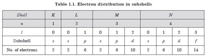
11 quantum numbers To understand the location and energy of each electron in an atom, one must have the knowledge of four quantum numbers: (i) Principal Quantum Number (n). This characterises the average distance of an electron from the nucleus and corresponds to the principal energy level in which electron resides. n can have positive integer values starting from 1, i.e. n = 1, 2, 3,.... The principal energy levels or shells having different values of n are designated by the letters K, L, M, N and so on. The maximum numbers of the electrons that can be accommodated in a shell corresponding to n is equal to 2n 22
12 (ii) Azimuthal Quantum Number (l). This is also called as orbital angular momentum quantum number and gives a measure of the angular momentum of an electron in the orbit. Physically, l indicates the shape of the classical orbit. For a given value of n, l can take all positive integer values from o to (n l). The particular l value defines the subshell, and the sub shells with l = 0, 1, 2, 3,... are designated as s, p, d, f, g,... respectively.
13 (iii) Magnetic Quantum Number (m l ). This is also called as orbital magnetic number and this determines the preferred orientation of the orbitals in space with respect to an applied magnetic field. We know that the magnetic moment of an electron due to its orbital motion gives rise to a magnetic field which can interact with an external magnetic field. The electrons orient themselves in certain preferred region of space around the nucleus under the influence of the external field. For a given value of l, can take integer values between ml 1 to + 1 including 0, i.e. total allowed values of are ml (2l + 1).
14 (iv) Spin Quantum Number (m s ). Electron is spinning about its own axis in the atom. The spin of the electron produces a spin magnetic moment which can either parallel or antiparallel to the surrounding magnetic field. For an electron there are two spin states. Spin quantum number is concerned with the spinning of the electron about its own axis. Thus m can take only two possible states, +½ or ½.
15 Pauli Exclusion Principle. This states that in an atom no two electrons can exist in the same quantum state, i.e. in an atom there cannot be two electrons with the same value of all the four quantum numbers. With the help of this principle, one can write the configuration of electrons. All the electrons with the same value of n constitute a shell and a shell can have a maximum of 2n 2 electrons.
16
17
18 Atomic structures of H, B, Si, P and Ge atoms.
19 The electrons in the inner shells of an atom do not normally leave the atom. But the electrons which are in the outermost shell, so called valence shell do not always remain confined to the same atom. Some of these valence electrons move in a random manner and may travel from one atom to another in a crystal lattice. These electrons are called as free electrons. It is due to the presence of these free electrons in a material, that electrical conduction is possible. The electrons in the inner orbits of the atom remain bound to the nucleus and are, therefore, called bound electrons.
20 chemical stability The tendency of an atom to give up its valence electrons depends on chemical stability. When an atom is stable, it resists giving up electrons, and when it is unstable, it tends to give up electrons. The level of stability is determined by the number of valence electrons, because the atom strives to have its outermost or valence shell completely filled.

21 Band formation
22 Classification of solids
23 Semiconductors Classification
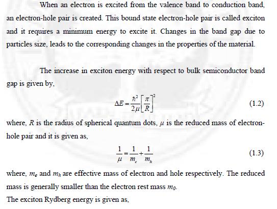
24 Exciton:
25 The exciton Rydberg energy is given as,
26 quantum confinement effect The tuning of fundamental properties such as optical and vibrational properties of nanostructured semiconductor material is possible when the size of the nanostructured semiconductor material approaches the exciton Bohr radius. Though significant variation in the fundamental properties is observed when the size is less than the exciton Bohr radius. This is due to the confinement of charge carriers and phonons within the nanoparticles. This is called quantum confinement effect. Efros and Efros (1982) introduced three regimes of quantum confinement, depending on the ratio of the nanocrystallite radius R to the Bohr radius of the electrons, holes and electron-hole pair.
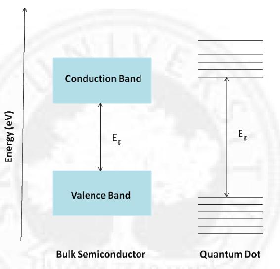
27
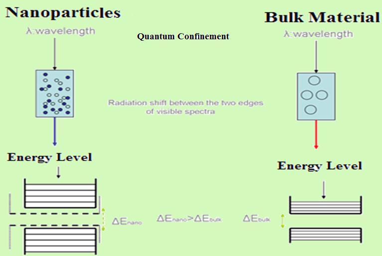
28 Quantum Confinement Surface to volume ratio
29 Semiconducting Materials Besides Elemental, Compund and Diluted Magnetic Semiconductors. Organic semiconductors: Semiconductor like properties are also found in "organic compounds" like polydiacetylene (CH2)n with conjugate carbon chains, fullerenes, nanotubes, BN nanotubes, etc. Organic molecules can easily be tailored at the molecular level and "tuned" for applications. However, these are not used too much, yet, but they seem promising materials for nonlinear optics (NLO), for example. Magnetic Semiconductors Strong magnetooptical effect allows the material to be used in optical modulators. Their Faraday rotation can be up to six orders of magnitude higher than that of nonmagnetic semiconductors. Magnetic field can also be used to cause the metal to semiconductor transition, a phenomenon also called colossal magnetoresistance. Other... Ferroelectric and complex inorganic materials... for NLO
30 Types of Semiconductor Materials The silicon doped with extra electrons is called an N type semiconductor. N is for negative, which is the charge of an electron. Silicon doped with material missing electrons that produce locations called holes is called P type semiconductor. P is for positive, which is the charge of a hole. A presentation of esyst.org
31 Current Flow in N-type Semiconductors The DC voltage source has a positive terminal that attracts the free electrons in the semiconductor and pulls them away from their atoms leaving the atoms charged positively. Electrons from the negative terminal of the supply enter the semiconductor material and are attracted by the positive charge of the atoms missing one of their electrons. Current (electrons) flows from the positive terminal to the negative terminal. A presentation of esyst.org
32 Current Flow in P-type Semiconductors Electrons from the negative supply terminal are attracted to the positive holes and fill them. The positive terminal of the supply pulls the electrons from the holes leaving the holes to attract more electrons. Current (electrons) flows from the negative terminal to the positive terminal. Inside the semiconductor current flow is actually by the movement of the holes from positive to negative. A presentation of esyst.org
33

34 Diamond In the diamond structure, the carbon atoms are arranged on an fcc-type lattice with a total of 16 electrons per primitive cell. The valence band and 7 lower bands are full, leaving no electrons in the conduction band.

35 Diamond Electrons may be thermally activated to jump a gap. At room temperature, k B T is only ev. To jump the energy gap, the electron requires very high temperatures. So, diamond is an excellent insulator. ρ = m
36 Graphite/Graphene ρ = 9 -m
 chance for a few electrons to be thermally excited from valence band to conduction")
37 Silicon Silicon has the diamond structure. There are 14 electrons per primitive cell. Gap is only 1.12 ev, however. Now there is a small (but finite) chance for a few electrons to be thermally excited from valence band to conduction band.

38 Silicon }1.12 ev
39 Effective Mass(m e ) Revisited An electron moving in the solid under the influence of the crystal potential is subjected to an electric field. We expect an external field to accelerate the electron, increasing E and k and change the electron s state. If this external field is much weaker than the internal field, the effect the latter is to modify the mass of carriers in such a way that the carriers respond to the applied field with this modified mass obeying classical mechanics. This modified mass is termed as effective mass of carriers and is usually different from electron mass (m 0 ) in vacuum.
40 Effective Mass Revisited m e d 2 dk This relates the curvature of the band to the effective mass. One can show that a free electron band gives an effective mass equal to the rest mass of an electron. Electrons in a crystal are accelerated in response to an external force just as though they were free electrons with effective mass m e. Usually, m e < m 0. 1
41 Effective Mass Revisited
42 Effective Mass Revisited Material Electron Effective Mass Hole Effective Mass Group IV Si (4.2 K) Ge Groups III-IV GaAs InSb Groups II-VI ZnO 0., ZnSe in multiples of the free electron mass m 0 = kg
43 Experimental Measurement Traditionally effective masses were measured using cyclotron resonance, a method in which microwave absorption of a semiconductor immersed in a magnetic field goes through a sharp peak when the microwave frequency equals the cyclotron frequency. In recent years effective masses have more commonly been determined through measurement of band structures using techniques such as angleresolved photoemission or, most directly, the de Haas-van Alphen effect. Effective masses can also be estimated using the coefficient g of the linear term in the low-temperature electronic specific heat at constant volume C v. The specific heat depends on the effective mass through the density of states at the Fermi level and as such is a measure of degeneracy as well as band curvature.
44 Electrons & Holes
45 Electrons & Holes For the electrons occupying the vacant states, d 2 dk (Negative!) and the electrons will move in same direction as electric field (wrong way!) 0 In a semiconductor, there are two charge carriers: Electrons (conduction band) negative mass negative charge Holes (valence band) positive mass, positive charge
46 Carrier Concentration To calculate the carrier concentrations in energy bands we need to know the following parameters: The distribution of energy states or levels as a function of energy within the energy band, D(). The probability of each of these states being occupied by an electron, f(). n f ( ) D( ) d c v p 1 f ( ) D( ) d
47 A band is shown for a one-dimensional crystal. The square represents an initially empty state in an otherwise filled band. When an electric field is applied, the states represented by arrows successsively become empty as electrons make transitions.

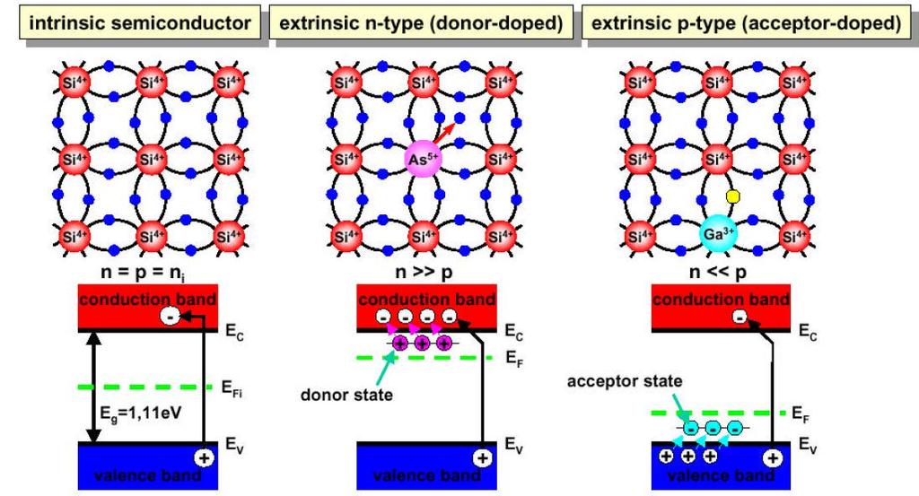
48 The band is completely filled except for a state marked by a square. Except for the electron represented as a circle, each electron can be paired with another, so the sum of their crystal momentum vanishes. The total crystal momentum for the band and the crystal momentum of the hole are both ħk.

49 The empty state and the unpaired electron for two times are shown when an electric field is applied. The change in momentum is in the direction of the field.
50 Conduction Band Carrier Concentration D( ) n f ( ) D( ) d 0 dn( ) 1 de 2 2m e 2 3 3/ 2 For >> F, the Boltzmann distribution approximates the F-D distribution: f ( ) 1 e 1 ( F )/ k B T e ( F )/ k B T e ( c )/ kbt which is valid for the tail end of the distribution. e ( cf )/ kbt
51 Conduction Band Carrier Concentration ( c F )/ kt B c/ kt B n e D( ) e d 0 N C 3/2 m 2 ekbt 2 2 n N C e / k T F c B

52 Conduction Band Carrier Concentration
53 Valence Band Carrier Concentration The hole distribution is related to the electron distribution, since a hole is the absence of an electron. f h 1 e f e F 1 / k B T 1 1 / kbt 1 / e F e F (as long as F kbt The holes near the top of the valence band behave like particles with effective mass m h ; and the density of states is 3/ 2 1 2mh D( ) 2 2 v 2 3/ 2 v m hkbt 2 p 1 f ( ) D( ) d 2 e 2 k 1 B T ) / kt v F B
54 Equilibrium Relation Multiply n and p together: np 4 k B T m The product is constant at a given temperature. It is also independent of any impurity concentration at a given temperature. This is because any impurity that adds electrons, necessarily fills holes. This is important in practice, since we could reduce the total carrier concentration n + p in an impure crystal via the controlled introduction of suitable impurities such reduction is called compensation. h m e 3/2 e / T g k B
55 Intrinsic Semiconductors n i p n v F F c v c B k B T F v v k B T c F c N N T k e N e N ln / / v c B v c F N N T k ln F c v
56 Extrinsic Semiconductors Extrinsic semiconductors: we can add impurities to make a material semiconducting (or to change the properties of the gap). There are 2 types of extrinsic semiconductors: p-type and n-type These are materials which have mostly hole carriers (p) or electron carriers (n). These give you ways of modifying the band gap energies (important for electronics, detectors, etc).
57 Extrinsic Semiconductors: n type Add a small amount of phosporus (P: 3s 2 3p 3 ) to Silicon (Si: 3s 2 3p 2 ) (generally, a group V element to a group IV host) P replaces a Si atom and it donates an electron to the conduction band (P is called the donor atom). The periodic potential is disrupted and we get a localized energy level, D. This is an n-type semiconductor more electrons around that can be mobile; and the Fermi energy is closer to the conduction band.
. Therefore, by doping Si crystal with phosphorus, we increase the free electron concentration.")
58 Extrinsic Semiconductors: n type Phosphorus provides an extra electron. C D = 45 mev So, its easy for the donor electrons to enter the conduction band at room temperature. This means that at room temperature n N D. This is called complete ionization (only true if n i << N D ). Therefore, by doping Si crystal with phosphorus, we increase the free electron concentration. At low temperature, these extra electrons get trapped at the donor sites (no longer very mobile) - the dopant is frozen out.

59 Extrinsic Semiconductors: p type Next suppose Si atom is replaced with Boron (B: 2s 2 2p) to Silicon (Si: 3s 2 3p 2 ). Again, we have a perturbed lattice and a localized E-level created. Boron is missing an electron and accepts an electron from valence band, creating a hole. Therefore doping with B increases hole concentration. We call this p-type doping, the electron concentration n is reduced. F moves closer to V. c F v A
60 Extrinsic Semiconductors
61 Extrinsic Semiconductors Boron in Silicon
62 Mass Action Law Valid for both intrinsic and extrinsic semiconductors. It is important in devices to control n and p concentrations and to suppress the influence of the intrinsic concentration. These equations are important in establishing upper limits in semiconductor operating temperature. We generally require n i << (minimum doping density) and, practically, this means we need doping concentrations above cm 3.
63 Semiconductors
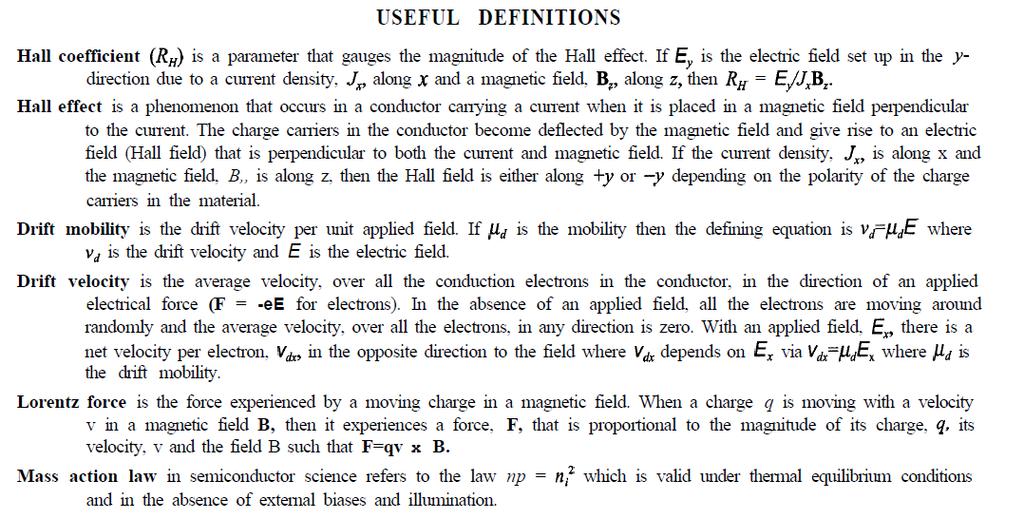
64 The Hall Effects

65 Discovery Observed in 1879 Edwin Herbert Hall Discovered 18 years before the electron Via Wikimedia Commons (public domain) The Hall effect was discovered in 1879 by Edwin Hall while he was working on his doctoral degree at Johns Hopkins University in Baltimore, Maryland. His measurements of the tiny effect produced in the apparatus he used were an experimental tour de force, accomplished 18 years before the electron was discovered and published under the name "On a New Action of the Magnet on Electric Currents". 65
66 Hall effect in Metals For a simple metal where there is only one type of charge carrier (electrons) the Hall voltage V H can be derived by using the Lorentz force and seeing that in the steady-state condition charges are not moving in the y-axis direction because the magnetic force on each electron in the y-axis direction is cancelled by a y- axis electrical force due to the buildup of charges.
67 Lorentz Force
68 Principles Mobile charges pressed to one side from Lorentz force, immobile charges unaltered Creates internal electric potential, known as Hall voltage. For simple metals, V H = Note: t refers to the thickness of the metal along the direction of the B- field 68
69 Concept: The Hall effect is due to the nature of the current in a conductor. Current consists of the movement of many small charge carriers, typically electrons, holes, ions (see Electromigration) or all three. When a magnetic field is present, these charges experience a force, called the Lorentz force. When such a magnetic field is absent, the charges follow approximately straight, 'line of sight' paths between collisions with impurities, phonons, etc. However, when a magnetic field with a perpendicular component is applied, their paths between collisions are curved so that moving charges accumulate on one face of the material. This leaves equal and opposite charges exposed on the other face, where there is a scarcity of mobile charges. The result is an asymmetric distribution of charge density across the Hall element, arising from a force that is perpendicular to both the 'line of sight' path and the applied magnetic field. The separation of charge establishes an electric field that opposes the migration of further charge, so a steady electrical potential is established for as long as the charge is flowing.

70 A Visual Representation Hall Effect measurement setup for electrons. Initially, the electrons follow the curved arrow, due to the magnetic force. At some distance from the current-introducing contacts, electrons pile up on the left side and deplete from the right side, which creates an electric field ξ y in the direction of the assigned V H. V H is negative for some semi-conductors where "holes" appear to flow. In steady-state, ξ y will be strong enough to exactly cancel out the magnetic force, so that the electrons follow the straight arrow (dashed). Richard Beck - Physics 141A,
71 Hall effect in semiconductors When a current-carrying semiconductor is kept in a magnetic field, the charge carriers of the semiconductor experience a force in a direction perpendicular to both the magnetic field and the current. At equilibrium, a voltage appears at the semiconductor edges. The simple formula for the Hall coefficient given above becomes more complex in semiconductors where the carriers are generally both electrons and holes which may be present in different concentrations and have different mobilities. For moderate magnetic fields the Hall coefficient is
72 Hall Coefficient Magnitude parameter: In metals: In semiconductors: 72
73 achievement Classical Picture: only electrons moving in same average direction in both hole (p-type) and electron (n-type) conductivity Opposite sign indicates that electrons in valence bands move in opposite direction than previously thought 73
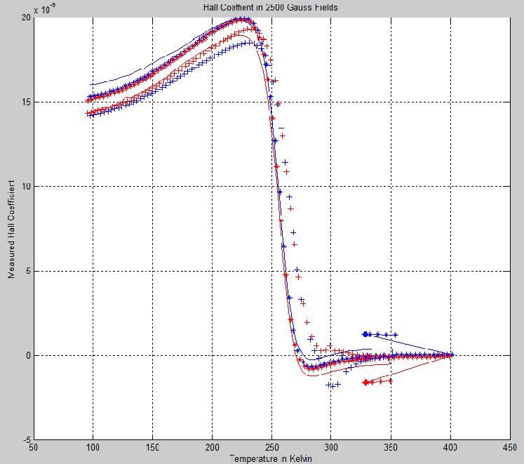
74 Applications Measurement can tell about charge carrier mobility and concentration. Conversely, knowing the above allows for sensitive measurement of an external B-field. Resistant to outside contaminants unlike optical, electromechanical testing. 74

75 Hall Probes Via LessEMF.com Via the NDT Resource Center 75
76 Rotation Sensing Hall Effect sensors capable of switching very fast, does not distort like capacitative or inductive sensors Contactless sensing 76

77 In Cars Used expansively in rotating systems Anti-lock brakes, motor feedback, ignition Via Power Systems Design, Ltd. Via Draper,


78 Hall Effect thruster In Space Trap electrons in a magnetic field, electrons ionize propellant, creates thrust 78
79 New Discoveries QuantumHall Effect Spin Hall Effect Anomalous Hall Effect 79
80 Quantum Hall Effect For a two-dimensional electron system which can be produced in a MOSFET, in the presence of large magnetic field strength and low temperature, one can observe the quantum Hall effect, in which the Hall conductance σ undergoes quantum Hall transitions to take on the quantized values. Quantization of normal Hall Effect Seen at low temperature, high magnetic field Very precise, magnitude determined by Landau levels and electron interaction 80
81 Spin Hall Effect Separation of electron spins in currentcarrying object, no magnetic field needed. Predicted in 1971, observed in 2004 via emission of circularly polarized light. Universal, present in metals and semiconductors at high and low temperature. 81

82 Anamolous (extraordinary) Hall Effect Ferromagnetic materials have internal magnetic field Much larger than normal Hall Effect, but not well understood. Via Toyosaki et al

83 Personal Experiments Aluminum-doped Germanium 1 sq cm chip Van Der Pauw configuration 83
84 Hall Coefficients 84

85 Extrapolated Carrier Mobility Clear temperature dependence! Has to do with electron energy 85
86 NOTATIONS
87
Resistance (R) Temperature (T)
 Temperature (T)") CHAPTER 1 Physical Properties of Elements and Semiconductors 1.1 Introduction Semiconductors constitute a large class of substances which have resistivities lying between those of insulators and conductors.
CHAPTER 1 Physical Properties of Elements and Semiconductors 1.1 Introduction Semiconductors constitute a large class of substances which have resistivities lying between those of insulators and conductors.
Atoms? All matters on earth made of atoms (made up of elements or combination of elements).
.") Chapter 1 Atoms? All matters on earth made of atoms (made up of elements or combination of elements). Atomic Structure Atom is the smallest particle of an element that can exist in a stable or independent
Chapter 1 Atoms? All matters on earth made of atoms (made up of elements or combination of elements). Atomic Structure Atom is the smallest particle of an element that can exist in a stable or independent
Chapter 1 Overview of Semiconductor Materials and Physics
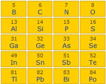
 Chapter 1 Overview of Semiconductor Materials and Physics Professor Paul K. Chu Conductivity / Resistivity of Insulators, Semiconductors, and Conductors Semiconductor Elements Period II III IV V VI 2 B
EXTRINSIC SEMICONDUCTOR
 EXTRINSIC SEMICONDUCTOR In an extrinsic semiconducting material, the charge carriers originate from impurity atoms added to the original material is called impurity [or] extrinsic semiconductor. This Semiconductor
EE301 Electronics I , Fall
 EE301 Electronics I 2018-2019, Fall 1. Introduction to Microelectronics (1 Week/3 Hrs.) Introduction, Historical Background, Basic Consepts 2. Rewiev of Semiconductors (1 Week/3 Hrs.) Semiconductor materials
Lecture 2. Semiconductor Physics. Sunday 4/10/2015 Semiconductor Physics 1-1
 Lecture 2 Semiconductor Physics Sunday 4/10/2015 Semiconductor Physics 1-1 Outline Intrinsic bond model: electrons and holes Charge carrier generation and recombination Intrinsic semiconductor Doping:
Electro - Principles I
 Electro - Principles I Page 10-1 Atomic Theory It is necessary to know what goes on at the atomic level of a semiconductor so the characteristics of the semiconductor can be understood. In many cases a
Introduction to Semiconductor Physics. Prof.P. Ravindran, Department of Physics, Central University of Tamil Nadu, India
 Introduction to Semiconductor Physics 1 Prof.P. Ravindran, Department of Physics, Central University of Tamil Nadu, India http://folk.uio.no/ravi/cmp2013 Review of Semiconductor Physics Semiconductor fundamentals
Lecture 1. OUTLINE Basic Semiconductor Physics. Reading: Chapter 2.1. Semiconductors Intrinsic (undoped) silicon Doping Carrier concentrations
 silicon Doping Carrier concentrations") Lecture 1 OUTLINE Basic Semiconductor Physics Semiconductors Intrinsic (undoped) silicon Doping Carrier concentrations Reading: Chapter 2.1 EE105 Fall 2007 Lecture 1, Slide 1 What is a Semiconductor? Low
Lecture 1 OUTLINE Basic Semiconductor Physics Semiconductors Intrinsic (undoped) silicon Doping Carrier concentrations Reading: Chapter 2.1 EE105 Fall 2007 Lecture 1, Slide 1 What is a Semiconductor? Low
Processing of Semiconducting Materials Prof. Pallab Banerji Department of Material Science Indian Institute of Technology, Kharagpur
 Processing of Semiconducting Materials Prof. Pallab Banerji Department of Material Science Indian Institute of Technology, Kharagpur Lecture - 4 Doping in Semiconductors Good morning. Let us start with
The Semiconductor in Equilibrium
 Lecture 6 Semiconductor physics IV The Semiconductor in Equilibrium Equilibrium, or thermal equilibrium No external forces such as voltages, electric fields. Magnetic fields, or temperature gradients are
CLASS 1 & 2 REVISION ON SEMICONDUCTOR PHYSICS. Reference: Electronic Devices by Floyd
 CLASS 1 & 2 REVISION ON SEMICONDUCTOR PHYSICS Reference: Electronic Devices by Floyd 1 ELECTRONIC DEVICES Diodes, transistors and integrated circuits (IC) are typical devices in electronic circuits. All
A semiconductor is an almost insulating material, in which by contamination (doping) positive or negative charge carriers can be introduced.
 positive or negative charge carriers can be introduced.") Semiconductor A semiconductor is an almost insulating material, in which by contamination (doping) positive or negative charge carriers can be introduced. Page 2 Semiconductor materials Page 3 Energy levels
Semiconductor A semiconductor is an almost insulating material, in which by contamination (doping) positive or negative charge carriers can be introduced. Page 2 Semiconductor materials Page 3 Energy levels
Basic Semiconductor Physics
 6 Basic Semiconductor Physics 6.1 Introduction With this chapter we start with the discussion of some important concepts from semiconductor physics, which are required to understand the operation of solar
ELECTRONIC DEVICES AND CIRCUITS SUMMARY
 ELECTRONIC DEVICES AND CIRCUITS SUMMARY Classification of Materials: Insulator: An insulator is a material that offers a very low level (or negligible) of conductivity when voltage is applied. Eg: Paper,
Ch. 2: Energy Bands And Charge Carriers In Semiconductors
 Ch. 2: Energy Bands And Charge Carriers In Semiconductors Discrete energy levels arise from balance of attraction force between electrons and nucleus and repulsion force between electrons each electron
Electronic Devices & Circuits
 Electronic Devices & Circuits For Electronics & Communication Engineering By www.thegateacademy.com Syllabus Syllabus for Electronic Devices Energy Bands in Intrinsic and Extrinsic Silicon, Carrier Transport,
EECS130 Integrated Circuit Devices
 EECS130 Integrated Circuit Devices Professor Ali Javey 8/30/2007 Semiconductor Fundamentals Lecture 2 Read: Chapters 1 and 2 Last Lecture: Energy Band Diagram Conduction band E c E g Band gap E v Valence
electronics fundamentals
 electronics fundamentals circuits, devices, and applications THOMAS L. FLOYD DAVID M. BUCHLA Lesson 1: Diodes and Applications Semiconductors Figure 1-1 The Bohr model of an atom showing electrons in orbits
Semiconductor Physics and Devices Chapter 3.
 Introduction to the Quantum Theory of Solids We applied quantum mechanics and Schrödinger s equation to determine the behavior of electrons in a potential. Important findings Semiconductor Physics and
Electronics The basics of semiconductor physics
 Electronics The basics of semiconductor physics Prof. Márta Rencz, Gergely Nagy BME DED September 16, 2013 The basic properties of semiconductors Semiconductors conductance is between that of conductors
Introduction to Electronics and Semiconductor
 Introduction to Electronics and Semiconductor 1 Chapter Objectives To study and understand basic electronics. To study and understand semiconductor principles. 2 Definition Electronics is the branch of
smal band gap Saturday, April 9, 2011
 small band gap upper (conduction) band empty small gap valence band filled 2s 2p 2s 2p hybrid (s+p)band 2p no gap 2s (depend on the crystallographic orientation) extrinsic semiconductor semi-metal electron
Conductivity and Semi-Conductors
 Conductivity and Semi-Conductors J = current density = I/A E = Electric field intensity = V/l where l is the distance between two points Metals: Semiconductors: Many Polymers and Glasses 1 Electrical Conduction
Chapter 4: Bonding in Solids and Electronic Properties. Free electron theory
 Chapter 4: Bonding in Solids and Electronic Properties Free electron theory Consider free electrons in a metal an electron gas. regards a metal as a box in which electrons are free to move. assumes nuclei
Engineering 2000 Chapter 8 Semiconductors. ENG2000: R.I. Hornsey Semi: 1
 Engineering 2000 Chapter 8 Semiconductors ENG2000: R.I. Hornsey Semi: 1 Overview We need to know the electrical properties of Si To do this, we must also draw on some of the physical properties and we
Lecture 7: Extrinsic semiconductors - Fermi level
 Lecture 7: Extrinsic semiconductors - Fermi level Contents 1 Dopant materials 1 2 E F in extrinsic semiconductors 5 3 Temperature dependence of carrier concentration 6 3.1 Low temperature regime (T < T
Minimal Update of Solid State Physics
 Minimal Update of Solid State Physics It is expected that participants are acquainted with basics of solid state physics. Therefore here we will refresh only those aspects, which are absolutely necessary
Microscopic Ohm s Law
 Microscopic Ohm s Law Outline Semiconductor Review Electron Scattering and Effective Mass Microscopic Derivation of Ohm s Law 1 TRUE / FALSE 1. Judging from the filled bands, material A is an insulator.
EE143 Fall 2016 Microfabrication Technologies. Evolution of Devices
 EE143 Fall 2016 Microfabrication Technologies Prof. Ming C. Wu wu@eecs.berkeley.edu 511 Sutardja Dai Hall (SDH) 1-1 Evolution of Devices Yesterday s Transistor (1947) Today s Transistor (2006) 1-2 1 Why
Classification of Solids
 Classification of Solids Classification by conductivity, which is related to the band structure: (Filled bands are shown dark; D(E) = Density of states) Class Electron Density Density of States D(E) Examples
ECE 442. Spring, Lecture -2
 ECE 442 Power Semiconductor Devices and Integrated circuits Spring, 2006 University of Illinois at Chicago Lecture -2 Semiconductor physics band structures and charge carriers 1. What are the types of
CLASS 12th. Semiconductors
 CLASS 12th Semiconductors 01. Distinction Between Metals, Insulators and Semi-Conductors Metals are good conductors of electricity, insulators do not conduct electricity, while the semiconductors have
Semiconductor physics I. The Crystal Structure of Solids
 Lecture 3 Semiconductor physics I The Crystal Structure of Solids 1 Semiconductor materials Types of solids Space lattices Atomic Bonding Imperfection and doping in SOLIDS 2 Semiconductor Semiconductors
Chemistry Instrumental Analysis Lecture 8. Chem 4631
 Chemistry 4631 Instrumental Analysis Lecture 8 UV to IR Components of Optical Basic components of spectroscopic instruments: stable source of radiant energy transparent container to hold sample device
Semiconductor Physics
 Semiconductor Physics Motivation Is it possible that there might be current flowing in a conductor (or a semiconductor) even when there is no potential difference supplied across its ends? Look at the
CME 300 Properties of Materials. ANSWERS: Homework 9 November 26, As atoms approach each other in the solid state the quantized energy states:
 CME 300 Properties of Materials ANSWERS: Homework 9 November 26, 2011 As atoms approach each other in the solid state the quantized energy states: are split. This splitting is associated with the wave
ELECTRONIC I Lecture 1 Introduction to semiconductor. By Asst. Prof Dr. Jassim K. Hmood
 ELECTRONIC I Lecture 1 Introduction to semiconductor By Asst. Prof Dr. Jassim K. Hmood SOLID-STATE ELECTRONIC MATERIALS Electronic materials generally can be divided into three categories: insulators,
HALL EFFECT IN SEMICONDUCTORS
 Warsaw University of Technology Faculty of Physics Physics Laboratory I P Andrzej Kubiaczyk 30 HALL EFFECT IN SEMICONDUCTORS 1. ackground 1.1. Electron motion in electric and magnetic fields A particle
Mat E 272 Lecture 25: Electrical properties of materials
 Mat E 272 Lecture 25: Electrical properties of materials December 6, 2001 Introduction: Calcium and copper are both metals; Ca has a valence of +2 (2 electrons per atom) while Cu has a valence of +1 (1
DO PHYSICS ONLINE ELECTRIC CURRENT FROM IDEAS TO IMPLEMENTATION ATOMS TO TRANSISTORS ELECTRICAL PROPERTIES OF SOLIDS
 DO PHYSICS ONLINE FROM IDEAS TO IMPLEMENTATION 9.4.3 ATOMS TO TRANSISTORS ELECTRICAL PROPERTIES OF SOLIDS ELECTRIC CURRENT Different substances vary considerably in their electrical properties. It is a
KATIHAL FİZİĞİ MNT-510
 KATIHAL FİZİĞİ MNT-510 YARIİLETKENLER Kaynaklar: Katıhal Fiziği, Prof. Dr. Mustafa Dikici, Seçkin Yayıncılık Katıhal Fiziği, Şakir Aydoğan, Nobel Yayıncılık, Physics for Computer Science Students: With
EXTRINSIC SEMICONDUCTOR
 EXTRINSIC SEMICONDUCTOR EXTRINSIC SEMICONDUCTOR A semiconductor in which the impurity atoms are added by doping process is called Extrinsic semiconductor. The addition of impurities increases the carrier
Introduction to Engineering Materials ENGR2000. Dr.Coates
 Introduction to Engineering Materials ENGR2000 Chapter 18: Electrical Properties Dr.Coates 18.2 Ohm s Law V = IR where R is the resistance of the material, V is the voltage and I is the current. l R A
First-Hand Investigation: Modeling of Semiconductors
 perform an investigation to model the behaviour of semiconductors, including the creation of a hole or positive charge on the atom that has lost the electron and the movement of electrons and holes in
Lecture 2 Electrons and Holes in Semiconductors
 EE 471: Transport Phenomena in Solid State Devices Spring 2018 Lecture 2 Electrons and Holes in Semiconductors Bryan Ackland Department of Electrical and Computer Engineering Stevens Institute of Technology
Review of Semiconductor Fundamentals
 ECE 541/ME 541 Microelectronic Fabrication Techniques Review of Semiconductor Fundamentals Zheng Yang (ERF 3017, email: yangzhen@uic.edu) Page 1 Semiconductor A semiconductor is an almost insulating material,
FREQUENTLY ASKED QUESTIONS February 21, 2017
 FREQUENTLY ASKED QUESTIONS February 21, 2017 Content Questions How do you place a single arsenic atom with the ratio 1 in 100 million? Sounds difficult to get evenly spread throughout. Yes, techniques
1 Review of semiconductor materials and physics
 Part One Devices 1 Review of semiconductor materials and physics 1.1 Executive summary Semiconductor devices are fabricated using specific materials that offer the desired physical properties. There are
Carrier Mobility and Hall Effect. Prof.P. Ravindran, Department of Physics, Central University of Tamil Nadu, India
 Carrier Mobility and Hall Effect 1 Prof.P. Ravindran, Department of Physics, Central University of Tamil Nadu, India http://folk.uio.no/ravi/semi2013 calculation Calculate the hole and electron densities
SOLID STATE PHYSICS. Second Edition. John Wiley & Sons. J. R. Hook H. E. Hall. Department of Physics, University of Manchester
 SOLID STATE PHYSICS Second Edition J. R. Hook H. E. Hall Department of Physics, University of Manchester John Wiley & Sons CHICHESTER NEW YORK BRISBANE TORONTO SINGAPORE Contents Flow diagram Inside front
Ga and P Atoms to Covalent Solid GaP
 Ga and P Atoms to Covalent Solid GaP Band Gaps in Binary Group III-V Semiconductors Mixed Semiconductors Affect of replacing some of the As with P in GaAs Band Gap (ev) (nm) GaAs 1.35 919 (IR) GaP 2.24
Chapter 12: Semiconductors
 Chapter 12: Semiconductors Bardeen & Shottky January 30, 2017 Contents 1 Band Structure 4 2 Charge Carrier Density in Intrinsic Semiconductors. 6 3 Doping of Semiconductors 12 4 Carrier Densities in Doped
SEMICONDUCTOR PHYSICS
 SEMICONDUCTOR PHYSICS by Dibyendu Chowdhury Semiconductors The materials whose electrical conductivity lies between those of conductors and insulators, are known as semiconductors. Silicon Germanium Cadmium
SEMICONDUCTORS. Conductivity lies between conductors and insulators. The flow of charge in a metal results from the
 SEMICONDUCTORS Conductivity lies between conductors and insulators The flow of charge in a metal results from the movement of electrons Electros are negatively charged particles (q=1.60x10⁻¹⁹ C ) The outermost
Semiconductors. Semiconductors also can collect and generate photons, so they are important in optoelectronic or photonic applications.
 Semiconductors Semiconducting materials have electrical properties that fall between true conductors, (like metals) which are always highly conducting and insulators (like glass or plastic or common ceramics)
Semiconductor Physics. Lecture 3
 Semiconductor Physics Lecture 3 Intrinsic carrier density Intrinsic carrier density Law of mass action Valid also if we add an impurity which either donates extra electrons or holes the number of carriers
Unit IV Semiconductors Engineering Physics
 Introduction A semiconductor is a material that has a resistivity lies between that of a conductor and an insulator. The conductivity of a semiconductor material can be varied under an external electrical
David J. Starling Penn State Hazleton PHYS 214
 Being virtually killed by a virtual laser in a virtual space is just as effective as the real thing, because you are as dead as you think you are. -Douglas Adams, Mostly Harmless David J. Starling Penn
Chapter Two. Energy Bands and Effective Mass
 Chapter Two Energy Bands and Effective Mass Energy Bands Formation At Low Temperature At Room Temperature Valence Band Insulators Metals Effective Mass Energy-Momentum Diagrams Direct and Indirect Semiconduction
3C3 Analogue Circuits
 Department of Electronic & Electrical Engineering Trinity College Dublin, 2014 3C3 Analogue Circuits Prof J K Vij jvij@tcd.ie Lecture 1: Introduction/ Semiconductors & Doping 1 Course Outline (subject
Semiconductors 1. Explain different types of semiconductors in detail with necessary bond diagrams. Intrinsic semiconductors:
 Semiconductors 1. Explain different types of semiconductors in detail with necessary bond diagrams. There are two types of semi conductors. 1. Intrinsic semiconductors 2. Extrinsic semiconductors Intrinsic
ECE 250 Electronic Devices 1. Electronic Device Modeling
 ECE 250 Electronic Devices 1 ECE 250 Electronic Device Modeling ECE 250 Electronic Devices 2 Introduction to Semiconductor Physics You should really take a semiconductor device physics course. We can only
SEMICONDUCTOR BEHAVIOR AND THE HALL EFFECT
 5 Feb 14 Semi.1 SEMICONDUCTOR BEHAVIOR AND THE HALL EFFECT The object of this experiment is to study various properties of n- and p-doped germanium crystals. The temperature dependence of the electrical
ITT Technical Institute ET215 Devices I Unit 1
 ITT Technical Institute ET215 Devices I Unit 1 Chapter 1 Chapter 2, Sections 2.1-2.4 Chapter 1 Basic Concepts of Analog Circuits Recall ET115 & ET145 Ohms Law I = V/R If voltage across a resistor increases
EECS143 Microfabrication Technology
 EECS143 Microfabrication Technology Professor Ali Javey Introduction to Materials Lecture 1 Evolution of Devices Yesterday s Transistor (1947) Today s Transistor (2006) Why Semiconductors? Conductors e.g
Materials Science. Atomic Structures and Bonding
 Materials Science Atomic Structures and Bonding 1 Atomic Structure Fundamental concepts Each atom consists of a nucleus composed of protons and neutrons which are encircled by electrons. Protons and electrons
Course overview. Me: Dr Luke Wilson. The course: Physics and applications of semiconductors. Office: E17 open door policy
 Course overview Me: Dr Luke Wilson Office: E17 open door policy email: luke.wilson@sheffield.ac.uk The course: Physics and applications of semiconductors 10 lectures aim is to allow time for at least one
MTLE-6120: Advanced Electronic Properties of Materials. Intrinsic and extrinsic semiconductors. Reading: Kasap:
 MTLE-6120: Advanced Electronic Properties of Materials 1 Intrinsic and extrinsic semiconductors Reading: Kasap: 5.1-5.6 Band structure and conduction 2 Metals: partially filled band(s) i.e. bands cross
From Last Time Important new Quantum Mechanical Concepts. Atoms and Molecules. Today. Symmetry. Simple molecules.
 Today From Last Time Important new Quantum Mechanical Concepts Indistinguishability: Symmetries of the wavefunction: Symmetric and Antisymmetric Pauli exclusion principle: only one fermion per state Spin
Lecture (02) Introduction to Electronics II, PN Junction and Diodes I
 Introduction to Electronics II, PN Junction and Diodes I") Lecture (02) Introduction to Electronics II, PN Junction and Diodes I By: Dr. Ahmed ElShafee ١ Agenda Current in semiconductors/conductors N type, P type semiconductors N Type Semiconductor P Type Semiconductor
Lecture (02) Introduction to Electronics II, PN Junction and Diodes I By: Dr. Ahmed ElShafee ١ Agenda Current in semiconductors/conductors N type, P type semiconductors N Type Semiconductor P Type Semiconductor
ADVANCED UNDERGRADUATE LABORATORY EXPERIMENT 20. Semiconductor Resistance, Band Gap, and Hall Effect
 ADVANCED UNDERGRADUATE LABORATORY EXPERIMENT 20 Semiconductor Resistance, Band Gap, and Hall Effect Revised: November 1996 by David Bailey March 1990 by John Pitre & Taek-Soon Yoon Introduction Solid materials
Calculating Band Structure
 Calculating Band Structure Nearly free electron Assume plane wave solution for electrons Weak potential V(x) Brillouin zone edge Tight binding method Electrons in local atomic states (bound states) Interatomic
Semiconductor Detectors
 Semiconductor Detectors Summary of Last Lecture Band structure in Solids: Conduction band Conduction band thermal conductivity: E g > 5 ev Valence band Insulator Charge carrier in conductor: e - Charge
Note that it is traditional to draw the diagram for semiconductors rotated 90 degrees, i.e. the version on the right above.
 5 Semiconductors The nearly free electron model applies equally in the case where the Fermi level lies within a small band gap (semiconductors), as it does when the Fermi level lies within a band (metal)
LECTURE 23. MOS transistor. 1 We need a smart switch, i.e., an electronically controlled switch. Lecture Digital Circuits, Logic
 LECTURE 23 Lecture 16-20 Digital Circuits, Logic 1 We need a smart switch, i.e., an electronically controlled switch 2 We need a gain element for example, to make comparators. The device of our dreams
Chapter 2. Semiconductor Fundamentals
 hapter Semiconductor Fundamentals.0 Introduction There are altogether 9 types of natural occurring elements, of which only few types are important in semiconductor physics and technology. They are the
Semiconductors. SEM and EDAX images of an integrated circuit. SEM EDAX: Si EDAX: Al. Institut für Werkstoffe der ElektrotechnikIWE
 SEM and EDAX images of an integrated circuit SEM EDAX: Si EDAX: Al source: [Cal 99 / 605] M&D-.PPT, slide: 1, 12.02.02 Classification semiconductors electronic semiconductors mixed conductors ionic conductors
CHAPTER 2: ENERGY BANDS & CARRIER CONCENTRATION IN THERMAL EQUILIBRIUM. M.N.A. Halif & S.N. Sabki
 CHAPTER 2: ENERGY BANDS & CARRIER CONCENTRATION IN THERMAL EQUILIBRIUM OUTLINE 2.1 INTRODUCTION: 2.1.1 Semiconductor Materials 2.1.2 Basic Crystal Structure 2.1.3 Basic Crystal Growth technique 2.1.4 Valence
Free Electron Model for Metals
 Free Electron Model for Metals Metals are very good at conducting both heat and electricity. A lattice of in a sea of electrons shared between all nuclei (moving freely between them): This is referred
Metals: the Drude and Sommerfeld models p. 1 Introduction p. 1 What do we know about metals? p. 1 The Drude model p. 2 Assumptions p.
 Metals: the Drude and Sommerfeld models p. 1 Introduction p. 1 What do we know about metals? p. 1 The Drude model p. 2 Assumptions p. 2 The relaxation-time approximation p. 3 The failure of the Drude model
Carriers Concentration in Semiconductors - V. Prof.P. Ravindran, Department of Physics, Central University of Tamil Nadu, India
 Carriers Concentration in Semiconductors - V 1 Prof.P. Ravindran, Department of Physics, Central University of Tamil Nadu, India http://folk.uio.no/ravi/semi2013 Motion and Recombination of Electrons and
collisions of electrons. In semiconductor, in certain temperature ranges the conductivity increases rapidly by increasing temperature
 1.9. Temperature Dependence of Semiconductor Conductivity Such dependence is one most important in semiconductor. In metals, Conductivity decreases by increasing temperature due to greater frequency of
Determination of properties in semiconductor materials by applying Matlab
 Determination of properties in semiconductor materials by applying Matlab Carlos Figueroa. 1, Raúl Riera A. 2 1 Departamento de Ingeniería Industrial. Universidad de Sonora A.P. 5-088, Hermosillo, Sonora.
Chapter 3 Properties of Nanostructures
 Chapter 3 Properties of Nanostructures In Chapter 2, the reduction of the extent of a solid in one or more dimensions was shown to lead to a dramatic alteration of the overall behavior of the solids. Generally,
EE 346: Semiconductor Devices
 EE 346: Semiconductor Devices Lecture - 5 02/01/2017 Tewodros A. Zewde 1 The One-Electron Atom The potential function is due to the coulomb attraction between the proton and electron and is given by where
Bohr s Model, Energy Bands, Electrons and Holes
 Dual Character of Material Particles Experimental physics before 1900 demonstrated that most of the physical phenomena can be explained by Newton's equation of motion of material particles or bodies and
Session 5: Solid State Physics. Charge Mobility Drift Diffusion Recombination-Generation
 Session 5: Solid State Physics Charge Mobility Drift Diffusion Recombination-Generation 1 Outline A B C D E F G H I J 2 Mobile Charge Carriers in Semiconductors Three primary types of carrier action occur
Diamond. Covalent Insulators and Semiconductors. Silicon, Germanium, Gray Tin. Chem 462 September 24, 2004
 Covalent Insulators and Chem 462 September 24, 2004 Diamond Pure sp 3 carbon All bonds staggered- ideal d(c-c) - 1.54 Å, like ethane Silicon, Germanium, Gray Tin Diamond structure Si and Ge: semiconductors
Review of Semiconductor Physics. Lecture 3 4 Dr. Tayab Din Memon
 Review of Semiconductor Physics Lecture 3 4 Dr. Tayab Din Memon 1 Electronic Materials The goal of electronic materials is to generate and control the flow of an electrical current. Electronic materials
Basic cell design. Si cell
 Basic cell design Si cell 1 Concepts needed to describe photovoltaic device 1. energy bands in semiconductors: from bonds to bands 2. free carriers: holes and electrons, doping 3. electron and hole current:
V = IR or R = V I. R = ρ l A
 Metals and Semiconductors Ram Seshadri MRL 2031, x6129, seshadri@mrl.ucsb.edu Electrical resistance and Ohm s Law: If an electric current I (units of A, Ampère) flows through a conductor with resistance
ECE440 Nanoelectronics. Lecture 07 Atomic Orbitals
 ECE44 Nanoelectronics Lecture 7 Atomic Orbitals Atoms and atomic orbitals It is instructive to compare the simple model of a spherically symmetrical potential for r R V ( r) for r R and the simplest hydrogen
Unit III Free Electron Theory Engineering Physics
 . Introduction The electron theory of metals aims to explain the structure and properties of solids through their electronic structure. The electron theory is applicable to all solids i.e., both metals
Chap. 1 (Introduction), Chap. 2 (Components and Circuits)
, Chap. 2 (Components and Circuits)") CHEM 455 The class describes the principles and applications of modern analytical instruments. Emphasis is placed upon the theoretical basis of each type of instrument, its optimal area of application,
CHEM 455 The class describes the principles and applications of modern analytical instruments. Emphasis is placed upon the theoretical basis of each type of instrument, its optimal area of application,
Concept of Core IENGINEERS- CONSULTANTS LECTURE NOTES SERIES ELECTRONICS ENGINEERING 1 YEAR UPTU. Page 1
 Concept of Core Conductivity of conductor and semiconductor can also be explained by concept of Core. Core: Core is a part of an atom other than its valence electrons. Core consists of all inner shells
Electrical Properties
 Electrical Properties Electrical Conduction R Ohm s law V = IR I l Area, A V where I is current (Ampere), V is voltage (Volts) and R is the resistance (Ohms or ) of the conductor Resistivity Resistivity,
Lecture 18: Semiconductors - continued (Kittel Ch. 8)
") Lecture 18: Semiconductors - continued (Kittel Ch. 8) + a - Donors and acceptors J U,e e J q,e Transport of charge and energy h E J q,e J U,h Physics 460 F 2006 Lect 18 1 Outline More on concentrations
Lecture 18: Semiconductors - continued (Kittel Ch. 8) + a - Donors and acceptors J U,e e J q,e Transport of charge and energy h E J q,e J U,h Physics 460 F 2006 Lect 18 1 Outline More on concentrations
Advantages / Disadvantages of semiconductor detectors
 Advantages / Disadvantages of semiconductor detectors Semiconductor detectors have a high density (compared to gas detector) large energy loss in a short distance diffusion effect is smaller than in gas
EE 446/646 Photovoltaic Devices I. Y. Baghzouz
 EE 446/646 Photovoltaic Devices I Y. Baghzouz What is Photovoltaics? First used in about 1890, the word has two parts: photo, derived from the Greek word for light, volt, relating to electricity pioneer