DIGITAL LOGIC DESIGN
|
|
|
- Lynette Waters
- 6 years ago
- Views:
Transcription

1 DIGITAL LOGIC DESIGN
2 NUMBERS SYSTEMS AND CODES
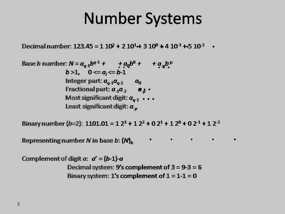
3 Any number in one base system can be converted into another base system Types 1) decimal to any base 2) Any base to decimal 3) Any base to Any base
4
5
6
7
8
9
10
11 Complements arc used in digital computers to simplify the subtraction operation and for log- ical manipulation They are two types of complements 1) Diminished radix complement (r n - 1)-N {r is the base of num system} 2) Radix Complement (r n - 1)-N+1
12 If the base = 10 The 9's complement of is = If the base = 2 The 1's complemcnt of is
13 the 10's complement of is the 1's complement of is
14 Discard end carry for r s complement Using 10's complement subtract M = 's complement of N = Sum = Discard end carry for 10 s complement Answer = 69282

15 X - Y = X = 's comp of Y = Sum = Add End-around carry = + 1 X - Y =
16
17
18
19

20
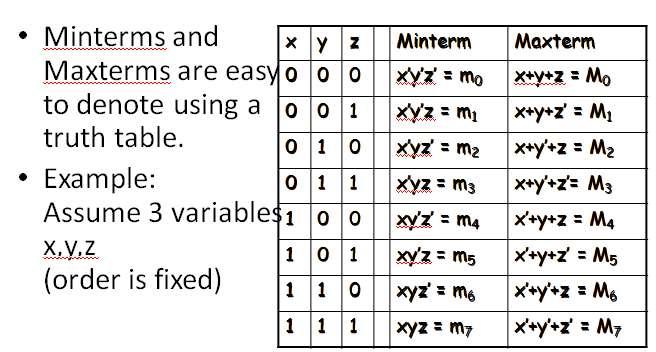
21 No communication channel or storage device is completely error-free As the number of bits per area or the transmission rate increases, more errors occur. Impossible to detect or correct 100% of the errors
22 - 3 Types of Error Detection/Correction Methods - Cyclic Redundancy Check (CRC) - Hamming Codes - Reed-Solomon (RS) = ^ ^ ^ Code word information error-checking bits/ bits parity bits/ syndrome/ redundant bits
23 One of the most effective codes for errorrecovery Used in situations where random errors are likely to occur Error detection and correction increases in proportion to the number of parity bits (errorchecking bits) added to the end of the information bits code word = information bits + parity bits Hamming distance: the number of bit positions in which two code words differ * * * Minimum Hamming distance or D(min) : determines its error detecting and correcting capability. Hamming codes can always detect D(min) 1 errors, but can only correct half of those errors.
24 EX. Data Parity Code Bits Bit Word * * * 011* 111
25 - Single parity bit can only detect error, not correct it - Error-correcting codes require more than a single parity bit EX Minimum Hamming distance = 3 Can detect up to 2 errors and correct 1 error
26 1. Let the information byte F = The sender and receiver agree on an arbitrary binary pattern P. Let P = Shift F to the left by 1 less than the number of bits in P. Now, F = Let F be the dividend and P be the divisor. Perform modulo 2 division. 5. After performing the division, we ignore the quotient. We got 100 for the remainder, which becomes the actual CRC checksum. 6. Add the remainder to F, giving the message M: = = M
27 7. M is decoded and checked by the message receiver using the reverse process Remainder
28 We need to consider formal techniques for the simplification of Boolean functions. Identical functions will have exactly the same canonical form. Minterms and Maxterms Sum-of-Minterms and Product-of- Maxterms Product and Sum terms Sum-of-Products (SOP) and Product-of-Sums (POS)
29 Literal: A variable or its complement Product term: literals connected by Sum term: literals connected by + Minterm: a product term in which all the variables appear exactly once, either complemented or uncomplemented Maxterm: a sum term in which all the variables appear exactly once, either complemented or uncomplemented
30
31 Any Boolean function F( ) can be expressed as a unique sum of minterms and a unique product of maxterms (under a fixed variable ordering). In other words, every function F() has two canonical forms: Canonical Sum-Of-Products (sum of minterms) Canonical Product-Of-Sums (product of maxterms)
32 Canonical Sum-Of-Products: The minterms included are those m j such that F( ) = 1 in row j of the truth table for F( ). Canonical Product-Of-Sums: The maxterms included are those M j such that F( ) = 0 in row j of the truth table for F( ).

33
34 Replace with (or vice versa) and replace those j s that appeared in the original form with those that do not. Example: f 1 (a,b,c) = a b c + a bc + ab c + abc = m 1 + m 2 + m 4 + m 6 = (1,2,4,6) = (0,3,5,7) = (a+b+c) (a+b +c ) (a +b+c ) (a +b +c )
35 Expand non-canonical terms by inserting equivalent of 1 in each missing variable x: (x + x ) = 1 Remove duplicate minterms f 1 (a,b,c) = a b c + bc + ac = a b c + (a+a )bc + a(b+b )c = a b c + abc + a bc + abc + ab c = a b c + abc + a bc + ab c
36 Expand noncanonical terms by adding 0 in terms of missing variables (e.g., xx = 0) and using the distributive law Remove duplicate maxterms f 1 (a,b,c) = (a+b+c) (b +c ) (a +c ) = (a+b+c) (aa +b +c ) (a +bb +c ) = (a+b+c) (a+b +c ) (a +b +c ) (a +b+c ) (a +b +c ) = (a+b+c) (a+b +c ) (a +b +c ) (a +b+c )

37
38 Formal logic: In formal logic, a statement (proposition) is a declarative sentence that is either true(1) or false (0). It is easier to communicate with computers using formal logic. Boolean variable: Takes only two values either true (1) or false (0). They are used as basic units of formal logic.
39 Boolean function: Mapping from Boolean variables to a Boolean value. Truth table: Represents relationship between a Boolean function and its binary variables. It enumerates all possible combinations of arguments and the corresponding function values.

40 Boolean algebra: Deals with binary variables and logic operations operating on those variables. Logic diagram: Composed of graphic symbols for logic gates. A simple circuit sketch that represents inputs and outputs of Boolean functions.
41 Refer to the hardware to implement Boolean operators. The most basic gates are
42
43 Postulate 1 (Definition): A Boolean algebra is a closed algebraic system containing a set K of two or more elements and the two operators and + which refer to logical AND and logical OR
44 (1) x + 0 = x (2) x 0 = 0 (3) x + 1 = 1 (4) x 1 = 1 (5) x + x = x (6) x x = x (7) x + x = x (8) x x = 0
45 (9) x + y = y + x (10) xy = yx (11) x + ( y + z ) = ( x + y ) + z (12) x (yz) = (xy) z (13) x ( y + z ) = xy + xz (14) x + yz = ( x + y )( x + z) (15) ( x + y ) = x y (16) ( xy ) = x + y (17) (x ) = x
46 Examples: (a) a + ab = a(1+b)=a (b) a(a + b) = a.a +ab=a+ab=a(1+b)=a. (c) a + a'b = (a + a')(a + b)=1(a + b) =a+b (d) a(a' + b) = a. a' +ab=0+ab=ab
47 (a) (a + b)' = a'b' (b) (ab)' = a' + b' Generalized DeMorgan's Theorem (a) (a + b + z)' = a'b' z' (b) (a.b z)' = a' + b' + z
48 F = ab + c d F =?? F = ab + c d + b d F =??
49 Show that: (a(b + z(x + a')))' =a' + b' (z' + x') (a(b + z(x + a')))' = a' + (b + z(x + a'))' = a' + b' (z(x + a'))' = a' + b' (z' + (x + a')') = a' + b' (z' + x'(a')') = a' + b' (z' + x'a) =a +b' z' + b'x'a =(a + b'x'a) + b' z' =(a + b'x )(a +a ) + b' z' = a + b'x + b' z = a' + b' (z' + x')
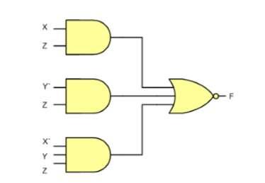
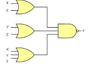
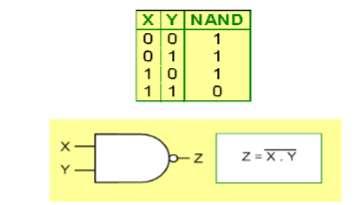
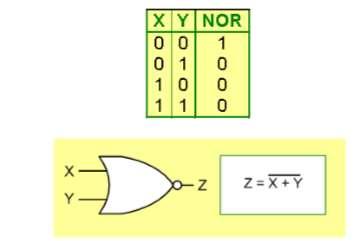
50 NAND-AND AND-NOR NOR-OR OR-NAND
51
52
53
54
55 The objectives of this lesson are to learn about: 1. Universal gates - NAND and NOR. 2. How to implement NOT, AND, and OR gate using NAND gates only. 3. How to implement NOT, AND, and OR gate using NOR gates only. 4. Equivalent gates.
56
57
58
59
60
61
62 BCD is a code for the decimal digits 0-9 Excess-3 is also a code for the decimal digits
63 Inputs: a BCD input, A,B,C,D with A as the most significant bit and D as the least significant bit. Outputs: an Excess-3 output W,X,Y,Z that corresponds to the BCD input. Internal operation circuit to do the conversion in combinational logic.
64 Excess-3 code is easily formed by adding a binary 3 to the binary or BCD for the digit. There are 16 possible inputs for both BCD and Excess-3. It can be assumed that only valid BCD inputs will appear so the six combinations not used can be treated as don t cares.
65 Lay out K-maps for each output, W X Y Z A step in the digital circuit design process.
66 Where are the Minterms located on a K-Map?
67 W(A,B,C,D) = Σm(5,6,7,8,9) +d(10,11,12,13,14,15) X(A,B,C,D) = Σm(1,2,3,4,9) +d(10,11,12,13,14,15) Y(A,B,C,D) = Σm(0,3,4,7,8) +d(10,11,12,13,14,15) Z(A,B,C,D) = Σm(0,2,4,6,8) +d(10,11,12,13,14,15)
68 W minimization Find W = A + BC + BD
69 X minimization Find X = BC D +B C+B D
70 Y minimization Find Y = CD + C D
71 Z minimization Find Z = D
72 Specification Digital readouts on many digital products often use LED seven-segment displays. Each digit is created by lighting the appropriate segments. The segments are labeled a,b,c,d,e,f,g The decoder takes a BCD input and outputs the correct code for the seven-segment display.
73 Input: A 4-bit binary value that is a BCD coded input. Outputs: 7 bits, a through g for each of the segments of the display. Operation: Decode the input to activate the correct segments.
74 Construct a truth table
75 Create a K-map for each output and get A = A C+A BD+B C D +AB C B = A B +A C D +A CD+AB C C = A B+A D+B C D +AB C D = A CD +A B C+B C D +AB C +A BC D E = A CD +B C D F = A BC +A C D +A BD +AB C G = A CD +A B C+A BC +AB C
76 Karnaugh Maps for Simplification 76
77 Boolean algebra helps us simplify expressions and circuits Karnaugh Map: A graphical technique for simplifying a Boolean expression into either form: minimal sum of products (MSP) minimal product of sums (MPS) Goal of the simplification. There are a minimal number of product/sum terms Each term has a minimal number of literals Circuit-wise, this leads to a minimal two-level implementation 77
78 A two-variable function has four possible minterms. We can rearrange these minterms into a Karnaugh map x y minterm 0 0 x y 0 1 x y 1 0 xy 1 1 xy X Y x y x y 1 xy xy Now we can easily see which minterms contain common literals Minterms on the left and right sides contain y and y respectively Minterms in the top and bottom rows contain x and x respectively X Y x y x y 1 xy xy Y Y X x y x y X xy xy 78
79 Imagine a two-variable sum of minterms: x y + x y Both of these Minterms appear in the top row of a Karnaugh map, which means that they both contain the literal x x y Y x y X xy xy x y + x y = x (y + y) [ Distributive ] = x 1 [ y + y = 1 ] = x [ x 1 = x ] What happens if you simplify this expression using Boolean algebra? 79
80 Another example expression is x y + xy Both minterms appear in the right side, where y is uncomplemented Thus, we can reduce x y + xy to just y x y Y x y X xy xy How about x y + x y + xy? We have x y + x y in the top row, corresponding to x There s also x y + xy in the right side, corresponding to y This whole expression can be reduced to x + y x y Y x y X xy xy 80
81 For a three-variable expression with inputs x, y, z, the arrangement of minterms is more tricky: YZ x y z x y z x yz x yz X 1 xy z xy z xyz xyz Y x y z x y z x yz x yz X xy z xy z xyz xyz Z YZ m 0 m 1 m 3 m 2 X 1 m4 m 5 m 7 m 6 Another way to label the K-map (use whichever you like): Y m 0 m 1 m 3 m 2 X m 4 m 5 m 7 m 6 Z 81
82 With this ordering, any group of 2, 4 or 8 adjacent squares on the map contains common literals that can be factored out Y x y z x y z x yz x yz X xy z xy z xyz xyz Z x y z + x yz = x z(y + y) = x z 1 = x z Adjacency includes wrapping around the left and right sides: Y x y z + xy z + x yz + xyz = z (x y + xy + x y + xy) x y z x y z x yz x yz = z (y (x + x) + y(x + x)) X xy z xy z xyz xyz = z (y +y) Z = z We ll use this property of adjacent squares to do our simplifications. 82
83 We can fill in the K-map directly from a truth table The output in row i of the table goes into square m i of the K-map Remember that the rightmost columns of the K-map are switched x y z f(x,y,z) Y X Z Y m 0 m 1 m 3 m 2 X m 4 m 5 m 7 m 6 Z 83
84 You can find the minimal SoP expression Each rectangle corresponds to one product term The product is determined by finding the common literals in that rectangle Y Y X Z x y z x y z x yz x yz X xy z xy z xyz xyz Z y z xy F(x,y,z)= y z + xy 84
85 The most difficult step is grouping together all the 1s in the K-map Make rectangles around groups of one, two, four or eight 1s All of the 1s in the map should be included in at least one rectangle Do not include any of the 0s Each group corresponds to one product term Y X Z 85
86 Make as few rectangles as possible, to minimize the number of products in the final expression. Make each rectangle as large as possible, to minimize the number of literals in each term. Rectangles can be overlapped, if that makes them larger. 86
 0 0 0 0 0 0 1 1 0 1 0 0 0 1 1 0 1 0 0 0")
87 Let s consider simplifying f(x,y,z) = xy + y z + xz You should convert the expression into a sum of minterms form, The easiest way to do this is to make a truth table for the function, and then read off the minterms You can either write out the literals or use the minterm shorthand Here is the truth table and sum of minterms for our example: x y z f(x,y,z) f(x,y,z) = x y z + xy z + xyz + xyz = m 1 + m 5 + m 6 + m 7 87
88 You can also convert the expression to a sum of minterms with Boolean algebra Apply the distributive law in reverse to add in missing variables. Very few people actually do this, but it s occasionally useful. xy + y z + xz = (xy 1) + (y z 1) + (xz 1) = (xy (z + z)) + (y z (x + x)) + (xz (y + y)) = (xyz + xyz) + (x y z + xy z) + (xy z + xyz) = xyz + xyz + x y z + xy z = m 1 + m 5 + m 6 + m 7 expression The resulting expression is larger than the original one! But having all the individual minterms makes it easy to combine them together with the K-map In both cases, we re actually unsimplifying our example 88
89 In our example, we can write f(x,y,z) in two equivalent ways f(x,y,z) = x y z + xy z + xyz + xyz Y x y z x y z x yz x yz X xy z xy z xyz xyz Z f(x,y,z) = m 1 + m 5 + m 6 + m 7 In either case, the resulting K-map is shown below Y m 0 m 1 m 3 m 2 X m 4 m 5 m 7 m 6 Z Y X Z 89
90 Simplify the sum of minterms m 1 + m 3 + m 5 + m 6 Y X Z Y m 0 m 1 m 3 m 2 X m 4 m 5 m 7 m 6 Z 90
91 Here is the filled in K-map, with all groups shown The magenta and green groups overlap, which makes each of them as large as possible Minterm m 6 is in a group all by its lonesome The final MSP here is x z + y z + xyz Y X Z 91
92 There may not necessarily be a unique MSP. The K-map below yields two valid and equivalent MSPs, because there are two possible ways to include minterm m 7 Y X Z Y X Z y z + yz + xy Y X Z y z + yz + xz Remember that overlapping groups is possible, as shown above 92
93 We can do four-variable expressions too! The minterms in the third and fourth columns, and in the third and fourth rows, are switched around. Again, this ensures that adjacent squares have common literals Grouping minterms is similar to the three-variable case, but: You can have rectangular groups of 1, 2, 4, 8 or 16 minterms You can wrap around all four sides 93
94 Y w x y z w x y z w x yz w x yz w xy z w xy z w xyz w xyz W wxy z wxy z wxyz wxyz wx y z wx y z wx yz wx yz Z X Y m 0 m 1 m 3 m 2 m 4 m 5 m 7 m 6 m 12 m 13 m 15 m 14 X W m8 m 9 m 11 m 10 Z 94

95 The expression is already a sum of minterms, so here s the K-map: Y X W Y m 0 m 1 m 3 m 2 m 4 m 5 m 7 m 6 m 12 m 13 m 15 m 14 X W m8 m 9 m 11 m 10 Z Z We can make the following groups, resulting in the MSP x z + xy z Y X W Z w x y z w x y z w x yz w x yz w xy z w xy z w xyz w xyz wxy z wxy z wxyz wxyz W wx y z wx y z wx yz wx yz Z Y X 95

96 W V= 0 V= 1Y Y m 16 m 17 m 19 m 8 m 20 m 21 m 23 m 22 X X m 28 m 29 m 31 m W 30 m24 m 25 m 27 m 26 Z m 0 m 1 m 3 m 2 m 4 m 5 m 7 m 6 m 12 m 13 m 15 m 14 m 8 m 9 m 11 m 10 Z 96
97 V= 0 V= 1 f = XZ Σm(4,6,12,14,20,22,28,30) + V W Y Σm(0,1,4,5) + W Y Z Σm(0,4,16,20) + VWXY Σm(30,31) + V WX YZ m11 97
98 Maxterms are grouped to find minimal PoS expression yz x 0 1 x +y+z x+y+z x+y +z x+y +z x +y+z x +y+z x +y +z x +y +z 98
99 F(W,X,Y,Z)= M(0,1,2,4,5) x 0 1 x +y+z x+y+z x+y +z x+y +z x +y+z x +y+z yz x +y +z 11 x +y +z 10 F(W,X,Y,Z)= Y. (X + Z) x yz
100 F(W,X,Y,Z)= Σm(0,1,2,5,8,9,10) = M(3,4,6,7,11,12,13,14,15) F(W,X,Y,Z)= (W + X )(Y + Z )(X + Z) Or, F(W,X,Y,Z)= X Y + X Z + W Y Z Which one is the minimal one? 10 0
101 F(W,X,Y,Z)= M(0,2,3,4,5,6) = Σm(1,7,8,9,10,11,12,13,14,15) 1 1 F(W,X,Y,Z)= W + XYZ + X Y Z
102 You don t always need all 2 n input combinations in an n-variable function If you can guarantee that certain input combinations never occur If some outputs aren t used in the rest of the circuit We mark don t-care outputs in truth tables and K-maps with Xs. x y z f(x,y,z) X X Within a K-map, each X can be considered as either 0 or 1. You should pick the interpretation that allows for the most simplification. 10 2
103 Find a MSP for f(w,x,y,z) = m(0,2,4,5,8,14,15), d(w,x,y,z) = m(7,10,13) This notation means that input combinations wxyz = 0111, 1010 and 1101 (corresponding to minterms m 7, m 10 and m 13 ) are unused. Y x 0 X 0 x 1 1 W x Z 10 3
104 Find a MSP for: f(w,x,y,z) = m(0,2,4,5,8,14,15), d(w,x,y,z) = m(7,10,13) Y x x 1 1 X W 1 x Z f(w,x,y,z)= x z + w xy + wxy 10 4
105 K-maps are an alternative to algebra for simplifying expressions The result is a MSP/MPS, which leads to a minimal two-level circuit It s easy to handle don t-care conditions K-maps are really only good for manual simplification of small expressions... Things to keep in mind: Remember the correct order of minterms/maxterms on the K-map When grouping, you can wrap around all sides of the K-map, and your groups can overlap Make as few rectangles as possible, but make each of them as large as possible. This leads to fewer, but simpler, product terms There may be more than one valid solution 10 5
106 UNIT 3
107 A process with 5 steps Specification Formulation Optimization Technology mapping Verification 1 st three steps and last best illustrated by example
108 Fundamental circuits that are the base building blocks of most larger digital circuits They are reusable and are common to many systems. Examples of functional logic circuits Decoders Encoders Code converters Multiplexers
109 Multiplexers Selectors for routing data to the processor, memory, I/O Multiplexers route the data to the correct bus or port. Decoders are used for selecting things like a bank of memory and then the address within the bank. This is also the function needed to decode the instruction to determine the operation to perform. Encoders are used in various components such as keyboards.
110 DESIGN OF SEQUENTIAL CIRCUITS
111 In this chapter you will learn about: Logic circuits that can store information Flip-flops, which store a single bit Registers, which store multiple bits Shift registers, which shift the contents of a register Counters of various types

112 Sensor Reset Set Memory element On Off Alarm Alarm turned on when On/Off = 1 Alarm turned off when On/Off = 0 Once triggered, alarm stays on until manually reset The circuit requires a memory element
113 Basic latch is a feedback connection of two NOR gates or two NAND gates It can store one bit of information It can be set to 1 using the S input and reset to 0 using the R input.
114 A B A feedback loop with even number of inverters If A = 0, B = 1 or when A = 1, B = 0 This circuit is not useful due to the lack of a mechanism for changing its state
115 Reset Set Q
116 Gated latch is a basic latch that includes input gating and a control signal The latch retains its existing state when the control input is equal to 0 Its state may be changed when the control signal is equal to 1. In our discussion we referred to the control input as the clock We consider two types of gated latches: Gated SR latch uses the S and R inputs to set the latch to 1 or reset it to 0, respectively. Gated D latch uses the D input to force the latch into a state that has the same logic value as the D input.
117
118
119 Setup Time t su The minimum time that the input signal must be stable prior to the edge of the clock signal. Hold Time t h The minimum time that the input signal must be stable after the edge of the clock signal. t su t h Clk D Q
120 A flip-flop is a storage element based on the gated latch principle It can have its output state changed only on the edge of the controlling clock signal
121 We consider two types: Edge-triggered flip-flop is affected only by the input values present when the active edge of the clock occurs Master-slave flip-flop is built with two gated latches The master stage is active during half of the clock cycle, and the slave stage is active during the other half. The output value of the flip-flop changes on the edge of the clock that activates the transfer into the slave stage.
122 D Master D Q Q m Slave D Q Q s Q Clock Clk Q Clk Q Q (a) Circuit Clock D Q m Q = Q s (b) Timing diagram D Q Q (c) Graphical symbol
123 D Q Clock Q Graphical symbol

124 Comparison of Level-Sensitive and Edge-Triggered D Storage Elements

125
126
127

128
 D flip-flop (Delay) JK")
129 SR flip-flop (Set, Reset) T flip-flop (Toggle) D flip-flop (Delay) JK flip-flop
130 Previous State -> Present State S R 0 -> 0 0 X 0 -> > > 1 X 0 Previous State -> Present State T 0 -> > > > 1 0
131 Previous State -> Present State D 0 -> > > > 1 1 Previous State -> Present State J K 0 -> 0 0 X 0 -> 1 1 X 1 -> 0 X 1 1 -> 1 X 0
132 S R 0->0 0 X 0-> > >1 X 0 CLK S R Q T 0->0 0 0->1 1 1->0 1 1->1 0 CLK T Q
133 D 0->0 0 0->1 1 1->0 0 1->1 1 CLK D Q J K 0->0 0 X 0->1 1 X 1->0 X 1 1->1 X 0 CLK J K Q
134 Procedure uses excitation tables Method: to realize a type A flipflop using a type B flipflop: 1. Start with the K-map or state-table for the A-flipflop. 2. Express B-flipflop inputs as a function of the inputs and present state of A-flipflop such that the required state transitions of A-flipflop are reallized. x Q g CL x Q y h CL y Type B Type A 1. Find Q + = f(g,h,q) for type A (using type A state-table) 2. Compute x = f1(g,h,q) and y=f2(g,h,q) to realize Q +.
135 Example: Use JK-FF to realize D-FF 1) Start transition table for D-FF 2) Create K-maps to express J and K as functions of inputs (D, Q) 3) Fill in K-maps with appropriate values for J and K to cause the same state transition as in the D-FF transition table D Q Q + J K X X X X 0 State-Table e.g. when D=Q=0, then Q + = 0 the same transition Q-->Q + is realize with J=0, K=X Q D Q Q R X X X S X J 0 1 X X D Q 0 1 K X X 1 0 X T X 1 0 D J = D K = D
136 Example: Implement JK-FF using a D-FF J K Q Q+ D T J K J K Clk D DFF C T T-FF Q Q JK Q 0 J JK Q 0 J Clk C K K d= jq + Kq t= jq + kq
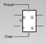
137 PRESET and CLEAR: asynchronous, level-sensitive inputs used to initialize a flipflop. PRESET, CLEAR: active low inputs Clk PRESET T Q CLEAR PRESET = 0 --> Q = 1 CLEAR = 0 --> Q = 0 LogicWorks Simulation SET 1 0 D S Q 0 1 T Q CRQ Clk 1 0 CLR Clk CLR SET T Q
138 Counters are a specific type of sequential circuit. Like registers, the state, or the flip-flop values themselves, serves as the output. The output value increases by one on each clock cycle. After the largest value, the output wraps around back to 0. Using two bits, we d get something like this: Present State Next State A B A B
139 Counters can act as simple clocks to keep track of time. You may need to record how many times something has happened. How many bits have been sent or received? How many steps have been performed in some computation? All processors contain a program counter, or PC. Programs consist of a list of instructions that are to be executed one after another (for the most part). The PC keeps track of the instruction currently being executed. The PC increments once on each clock cycle, and the next program instruction is then executed.
140 Let s try to design a slightly different two-bit counter: Again, the counter outputs will be 00, 01, 10 and 11. Now, there is a single input, X. When X=0, the counter value should increment on each clock cycle. But when X=1, the value should decrement on successive cycles. We ll need two flip-flops again. Here are the four possible states:
141 Here s the complete state diagram and state table for this circuit Present State Inputs Next State Q 1 Q 0 X Q 1 Q
142 If we use D flip-flops, then the D inputs will just be the same as the desired next states. Equations for the D flip-flop inputs are shown at the right. Why does D 0 = Q 0 make sense? Present State Inputs Next State Q 1 Q 0 X Q 1 Q Q Q X D 1 = Q 1 Q 0 X Q Q X D 0 = Q 0
143 Here are some D Flip Flop devices from LogicWorks. They have both normal and complemented outputs, so we can access Q0 directly without using an inverter. (Q1 is not needed in this example.) This circuit counts normally when Reset = 1. But when Reset is 0, the flip-flop outputs are cleared to 00 immediately. There is no three-input XOR gate in LogicWorks so we ve used a four-input version instead, with one of the inputs connected to 0.
144 If we use JK flip-flops instead, then we have to compute the JK inputs for each flip-flop. Look at the present and desired next state, and use the excitation table on the right. Q(t) Q(t+1) J K x x 1 0 x x 0 Present State Inputs Next State Flip flop inputs Q 1 Q 0 X Q 1 Q 0 J 1 K 1 J 0 K x 1 x x 1 x x x x x x 0 1 x x 1 1 x x 1 x x 0 x 1
145 Present State Inputs Next State Flip flop inputs Q 1 Q 0 X Q 1 Q 0 J 1 K 1 J 0 K x 1 x x 1 x x x x x x 0 1 x x 1 1 x x 1 x x 0 x 1 We can then find equations for all four flip-flop inputs, in terms of the present state and inputs. Here, it turns out J 1 = K 1 and J 0 = K 0. J 1 = K 1 = Q 0 X + Q 0 X J 0 = K 0 = 1
146 Here is the counter again, but using JK Flip Flop n.i. RS devices instead. The direct inputs R and S are noninverted, or active-high. So this version of the circuit counts normally when Reset = 0, but initializes to 00 when Reset is 1.
147 This counter is called asynchronous because not all flip flops are hooked to the same clock. Look at the waveform of the output, Q, in the timing diagram. It resembles a clock as well. If the period of the clock is T, then what is the period of Q, the output of the flip flop? It's 2T! We have a way to create a clock that runs twice as slow. We feed the clock into a T flip flop, where T is hardwired to 1. The output will be a clock who's period is twice as long.
148 If the clock has period T. Q0 has period 2T. Q1 period is 4T With n flip flops the period is 2 n.
149

150 This is called as a ripple counter due to the way the FFs respond one after another in a kind of rippling effect.
151 To eliminate the "ripple" effects, use a common clock for each flip-flop and a combinational circuit to generate the next state. For an up-counter, use an incrementer => Incrementer A3 A2 A1 A0 S3 S2 S1 S0 D3 D2 D1 D0 Q3 Q2 Q1 Q0 Clock

152 Internal details => Internal Logic Incrementer XOR complements each bit AND chain causes complement of a bit if all bits toward LSB from it equal 1 Count Enable Forces all outputs of AND chain to 0 to hold the state Carry Out Added as part of incrementer Connect to Count Enable of additional 4-bit counters to form larger counters
153 Use the sequential logic model to design a synchronous BCD counter with D flip-flops State Table => Input combinations 1010 through 1111 are don t cares Current State Q8 Q4 Q2 Q1 Next State Q8 Q4 Q2 Q
154 Use K-Maps to two-level optimize the next state equations and manipulate into forms containing XOR gates: D1 = Q1 D2 = Q2 + Q1Q8 D4 = Q4 + Q1Q2 D8 = Q8 + (Q1Q8 + Q1Q2Q4) Y = Q1Q8 The logic diagram can be drawn from these equations An asynchronous or synchronous reset should be added What happens if the counter is perturbed by a power disturbance or other interference and it enters a state other than 0000 through 1001?
155 Find the actual values of the six next states for the don t care combinations from the equations Find the overall state diagram to assess behavior for the don t care states (states in decimal) Present State Next State Q8 Q4 Q2 Q1 Q8 Q4 Q2 Q
156 For the BCD counter design, if an invalid state is entered, return to a valid state occurs within two clock cycles Is this adequate?!
157
158 The examples shown so far have all had 2 n states, and used n flip-flops. But sometimes you may have unused, leftover states. For example, here is a state table and diagram for a counter that repeatedly counts from 0 (000) to 5 (101). What should we put in the table for the two unused states? Present State Next State Q 2 Q 1 Q 0 Q 2 Q 1 Q ??? 1 1 1???
, its behavior Q 2 Q 1 will Qdepend 0 Q 2 on Qexactly 1 Q 0 what the don t cares were filled in with.")
159 To get the simplest possible circuit, you can fill in don t cares for the next states. This will also result in don t cares for the flip-flop inputs, which can simplify the hardware. If Present the circuit State somehow Next ends State up in one of the unused states (110 or 111), its behavior Q 2 Q 1 will Qdepend 0 Q 2 on Qexactly 1 Q 0 what the don t cares were filled in with x x x x x x 011
160 To get the safest possible circuit, you can explicitly fill in next states for the unused states 110 and 111. This guarantees that even if the circuit somehow enters an unused state, it will eventually end up in a valid state. This is called a self-starting counter. Present State Next State Q 2 Q 1 Q 0 Q 2 Q 1 Q
161 There are a couple of different counters available in LogicWorks. The simplest one, the Counter-4 Min, just increments once on each clock cycle. This is a four-bit counter, with values ranging from 0000 to The only input is the clock signal.
162 More complex counters are also possible. The full-featured LogicWorks Counter-4 device below has several functions. It can increment or decrement, by setting the UP input to 1 or 0. You can immediately (asynchronously) clear the counter to 0000 by setting CLR = 1. You can specify the counter s next output by setting D 3 -D 0 to any four-bit value and clearing LD. The active-low EN input enables or disables the counter. When the counter is disabled, it continues to output the same value without incrementing, decrementing, loading, or clearing. The counter out CO is normally 1, but becomes 0 when the counter reaches its maximum value, 1111.
163 As you might expect by now, we can use these general counters to build other counters. Here is an 8-bit counter made from two 4-bit counters. The bottom device represents the least significant four bits, while the top counter represents the most significant four bits. When the bottom counter reaches 1111 (i.e., when CO = 0), it enables the top counter for one cycle. Other implementation notes: The counters share clock and clear signals.
164 We can also make a counter that starts at some value besides In the diagram below, when CO=0 the LD signal forces the next state to be loaded from D 3 -D 0. The result is this counter wraps from 1111 to 0110 (instead of 0000).
165 We can also make a circuit that counts up to only 1100, instead of Here, when the counter value reaches 1100, the NAND gate forces the counter to load, so the next state becomes 0000.
166 Counters serve many purposes in sequential logic design. There are lots of variations on the basic counter. Some can increment or decrement. An enable signal can be added. The counter s value may be explicitly set. There are also several ways to make counters. You can follow the sequential design principles to build counters from scratch. You could also modify or combine existing counter devices.
167 Creating a sequential circuit to address a design need.
168 Steps in the design process for sequential circuits State Diagrams and State Tables Examples
169 Steps in Design of a Sequential Circuit 1. Specification A description of the sequential circuit. Should include a detailing of the inputs, the outputs, and the operation. Possibly assumes that you have knowledge of digital system basics. 2. Formulation: Generate a state diagram and/or a state table from the statement of the problem. 3. State Assignment: From a state table assign binary codes to the states. 4. Flip-flop Input Equation Generation: Select the type of flip-flop for the circuit and generate the needed input for the required state transitions
170 5. Output Equation Generation: Derive output logic equations for generation of the output from the inputs and current state. 6. Optimization: Optimize the input and output equations. Today, CAD systems are typically used for this in real systems. 7. Technology Mapping: Generate a logic diagram of the circuit using ANDs, ORs, Inverters, and F/Fs. 8. Verification: Use a HDL to verify the design.
171 Sequential machines are typically classified as either a Mealy machine or a Moore machine implementation. Moore machine: The outputs of the circuit depend only upon the current state of the circuit. Mealy machine: The outputs of the circuit depend upon both the current state of the circuit and the inputs.

172 The specification: The circuit will have one input, X, and one output, Z. The output Z will be 0 except when the input sequence 1101 are the last 4 inputs received on X. In that case it will be a 1.
173 Create states and meaning for them. State A the last input was a 0 and previous inputs unknown. Can also be the reset state. State B the last input was a 1 and the previous input was a 0. The start of a new sequence possibly. Capture this in a state diagram
174 Capture this in a state diagram Circles represent the states Lines and arcs represent the transition between state. The notation Input/Output on the line or arc specifies the input that causes this transition and the output for this change of state.
175 Add a state C State C Have detected the input sequence 11 which is the start of the sequence.
176 Add a state D State D have detected the 3 rd input in the start of a sequence, a 0, now having 110. From State D, if the next input is a 1 the sequence has been detected and a 1 is output.
177 The previous diagram was incomplete. In each state the next input could be a 0 or a 1. This must be included.
178 The state table This can be done directly from the state diagram. Now need to do a state assignment
179 Will select a gray encoding For this state A will be encoded 00, state B 01, state C 11 and state D 10
180 Generate the equations for the flip-flop inputs Generate the D 0 equation Generate the D 1 equation
181 The next step is to generate the equation for the output Z and what is needed to generate it. Create a K-map from the truth table.
182 The circuit has 2 D type F/Fs

183 UNIT 5
184 Data Storage (Volatile) Locations (Address) Byte or Word Data input Address Read Write Memory unit 16 x 8 Data output 18 4 / 18
185 Data Storage (Volatile) Locations (Address) Byte or Word m Data input 10 Address lines 1024 locations = 1 K k Address Read Write Memory unit 2 k x m m Data output 18 5 / 18
186 Memory Cell Select Input BC Output Select Read/Write Input S Q Output R Q Read/Write 18 6 / 18
187 Memory Array AddressL ines Memory Enable Read/Write I 1 I 0 2 x 4 Decoder E Input Data BC BC BC BC BC BC BC BC BC BC BC BC BC BC BC BC 18 7 / 18
188 k Address Memory Enable ROM 2 k x m m Data output 18 8 / 18
189 Conventional Symbol Array Logic Symbol 18 9 / 18
190 8 x 4 ROM AddressL ines Memory Enable 3 x 8 Decoder I 2 I 1 I 0 E Output Data 19 0 / 18
191 8 x 4 ROM Address Data A 2 A 1 A x 8 Decoder I 2 I 1 I 0 E D 3 D 2 D 1 D / 18
192 Mask Programmed ROM Programmed during manufacturing Programmable Read-Only Memory (PROM) Blow out fuses to produce 0 Erasable Programmable ROM (EPROM) Erase all data by Ultra Violet exposure Electrically Erasable PROM (EEPROM) Erase the required data using an electrical signal 19 2 / 18
193 Boolean Functions: Sums-of-Products AND-plane followed by OR-plane Y 7 Y 6 Y 5 Y 4 Y 3 Y 2 Y 1 Y 0 I 2 I 1 I / 18
194 PROM Inputs PAL Fixed AND array (Decoder) Programmable OR array Outputs Inputs PLA Programmable AND array Fixed OR array Outputs Inputs Programmable AND array Programmable OR array Outputs 19 4 / 18
195 Example w(a,b,c,d) = (2,12,13) x(a,b,c,d) = (7,8,9,10,11,12,13,14,15) F 1 w y(a,b,c,d) = (0,2,3,4,5,6,7,8,10,11,15) A I 1 z(a,b,c,d) = (1,2,8,12,13) Simplify: 4 5 F 2 x w = ABC + A B CD x = A + BCD y = A B + CD + B D B I 2 z = ABC + A B CD + AC D + A B C D = w + AC D + A B C D C I F 3 y F 4 z 12 D I / 18
196 A B C I 1 I 2 I 3 Example: F 1 = AB + AC + A BC F 2 = (AC + BC) 0 1 F 1 F / 18
197 Basic Macrocell Logic CLK OE D Q ENB Q 19 7 / 18
198 The following memory units are specified by the number of words times the number of bits per word. How many address lines and input-output lines are needed in each case? (a) 4K 16, (b) 2G 8, (c) 16M 32, (d) 256K 64. Give the number of bytes stored in the memories listed in Problem 7-1. Word number 723 in a memory of contains the binary equivalent of 3,451. List the 10-bit address and the 16-bit memory content of the word / 18
199 Specify the size of a ROM (number of words and number of bits per word) that will accommodate the truth table for the following combinational circuit components: (a) a binary multiplier that multiplies two 4-bit, (b) a 4-bit adder-subtractor, (c) a quadruple 2-to-1-line multiplexers with common select and enable inputs, and (d) a BCD-to-seven-segment decoder with an enable input / 18
200 Tabulate the truth table for an 8 4 ROM that implements the Boolean functions A(x,y,z) = (1,2,4,6) B(x,y,z) = (0,1,6,7) C(x,y,z) = (2,6) D(x,y,z) = (1,2,3,5,7) 20 0 / 18
Counters. We ll look at different kinds of counters and discuss how to build them
 Counters We ll look at different kinds of counters and discuss how to build them These are not only examples of sequential analysis and design, but also real devices used in larger circuits 1 Introducing
( c) Give logic symbol, Truth table and circuit diagram for a clocked SR flip-flop. A combinational circuit is defined by the function
 Give logic symbol, Truth table and circuit diagram for a clocked SR flip-flop. A combinational circuit is defined by the function") Question Paper Digital Electronics (EE-204-F) MDU Examination May 2015 1. (a) represent (32)10 in (i) BCD 8421 code (ii) Excess-3 code (iii) ASCII code (b) Design half adder using only NAND gates. ( c)
Question Paper Digital Electronics (EE-204-F) MDU Examination May 2015 1. (a) represent (32)10 in (i) BCD 8421 code (ii) Excess-3 code (iii) ASCII code (b) Design half adder using only NAND gates. ( c)
KUMARAGURU COLLEGE OF TECHNOLOGY COIMBATORE
 Estd-1984 KUMARAGURU COLLEGE OF TECHNOLOGY COIMBATORE 641 006 QUESTION BANK UNIT I PART A ISO 9001:2000 Certified 1. Convert (100001110.010) 2 to a decimal number. 2. Find the canonical SOP for the function
Department of Electrical & Electronics EE-333 DIGITAL SYSTEMS
 Department of Electrical & Electronics EE-333 DIGITAL SYSTEMS 1) Given the two binary numbers X = 1010100 and Y = 1000011, perform the subtraction (a) X -Y and (b) Y - X using 2's complements. a) X = 1010100
Boolean Algebra and Digital Logic 2009, University of Colombo School of Computing
 IT 204 Section 3.0 Boolean Algebra and Digital Logic Boolean Algebra 2 Logic Equations to Truth Tables X = A. B + A. B + AB A B X 0 0 0 0 3 Sum of Products The OR operation performed on the products of
Reg. No. Question Paper Code : B.E./B.Tech. DEGREE EXAMINATION, NOVEMBER/DECEMBER Second Semester. Computer Science and Engineering
 Sp 6 Reg. No. Question Paper Code : 27156 B.E./B.Tech. DEGREE EXAMINATION, NOVEMBER/DECEMBER 2015. Second Semester Computer Science and Engineering CS 6201 DIGITAL PRINCIPLES AND SYSTEM DESIGN (Common
DHANALAKSHMI COLLEGE OF ENGINEERING, CHENNAI DEPARTMENT OF COMPUTER SCIENCE AND ENGINEERING CS6201 DIGITAL PRINCIPLES AND SYSTEM DESIGN
 DHANALAKSHMI COLLEGE OF ENGINEERING, CHENNAI DEPARTMENT OF COMPUTER SCIENCE AND ENGINEERING CS6201 DIGITAL PRINCIPLES AND SYSTEM DESIGN UNIT I : BOOLEAN ALGEBRA AND LOGIC GATES PART - A (2 MARKS) Number
Fundamentals of Boolean Algebra
 UNIT-II 1 Fundamentals of Boolean Algebra Basic Postulates Postulate 1 (Definition): A Boolean algebra is a closed algebraic system containing a set K of two or more elements and the two operators and
 vidyarthiplus.com vidyarthiplus.com vidyarthiplus.com ANNA UNIVERSITY- COMBATORE B.E./ B.TECH. DEGREE EXAMINATION - JUNE 2009. ELECTRICAL & ELECTONICS ENGG. - FOURTH SEMESTER DIGITAL LOGIC CIRCUITS PART-A
Synchronous Sequential Logic
 1 IT 201 DIGITAL SYSTEMS DESIGN MODULE4 NOTES Synchronous Sequential Logic Sequential Circuits - A sequential circuit consists of a combinational circuit and a feedback through the storage elements in
LOGIC CIRCUITS. Basic Experiment and Design of Electronics
 Basic Experiment and Design of Electronics LOGIC CIRCUITS Ho Kyung Kim, Ph.D. hokyung@pusan.ac.kr School of Mechanical Engineering Pusan National University Outline Combinational logic circuits Output
ECEN 248: INTRODUCTION TO DIGITAL SYSTEMS DESIGN. Week 9 Dr. Srinivas Shakkottai Dept. of Electrical and Computer Engineering
 ECEN 248: INTRODUCTION TO DIGITAL SYSTEMS DESIGN Week 9 Dr. Srinivas Shakkottai Dept. of Electrical and Computer Engineering TIMING ANALYSIS Overview Circuits do not respond instantaneously to input changes
Digital Logic Appendix A
 Digital Logic Appendix A Boolean Algebra Gates Combinatorial Circuits Sequential Circuits 1 Boolean Algebra George Boole ideas 1854 Claude Shannon, apply to circuit design, 1938 Describe digital circuitry
Boolean Algebra. Digital Logic Appendix A. Postulates, Identities in Boolean Algebra How can I manipulate expressions?
 Digital Logic Appendix A Gates Combinatorial Circuits Sequential Circuits Other operations NAND A NAND B = NOT ( A ANDB) = AB NOR A NOR B = NOT ( A ORB) = A + B Truth tables What is the result of the operation
CHAPTER1: Digital Logic Circuits Combination Circuits
 CS224: Computer Organization S.KHABET CHAPTER1: Digital Logic Circuits Combination Circuits 1 PRIMITIVE LOGIC GATES Each of our basic operations can be implemented in hardware using a primitive logic gate.
Contents. Chapter 3 Combinational Circuits Page 1 of 36
 Chapter 3 Combinational Circuits Page of 36 Contents Combinational Circuits...2 3. Analysis of Combinational Circuits...3 3.. Using a Truth Table...3 3..2 Using a Boolean Function...6 3.2 Synthesis of
MC9211 Computer Organization
 MC92 Computer Organization Unit : Digital Fundamentals Lesson2 : Boolean Algebra and Simplification (KSB) (MCA) (29-2/ODD) (29 - / A&B) Coverage Lesson2 Introduces the basic postulates of Boolean Algebra
Digital Logic Design. Combinational Logic
 Digital Logic Design Combinational Logic Minterms A product term is a term where literals are ANDed. Example: x y, xz, xyz, A minterm is a product term in which all variables appear exactly once, in normal
EE40 Lec 15. Logic Synthesis and Sequential Logic Circuits
 EE40 Lec 15 Logic Synthesis and Sequential Logic Circuits Prof. Nathan Cheung 10/20/2009 Reading: Hambley Chapters 7.4-7.6 Karnaugh Maps: Read following before reading textbook http://www.facstaff.bucknell.edu/mastascu/elessonshtml/logic/logic3.html
Common Number Systems
 Number Systems Common Number Systems System Base Symbols Used by humans? Used in computers? Decimal 10 0, 1, 9 Yes No Binary 2 0, 1 No Yes Octal 8 0, 1, 7 No No Hexadecimal 16 0, 1, 9, A, B, F No No Conversion
Vidyalankar S.E. Sem. III [CMPN] Digital Logic Design and Analysis Prelim Question Paper Solution
![Vidyalankar S.E. Sem. III [CMPN] Digital Logic Design and Analysis Prelim Question Paper Solution](/thumbs/90/103673562.jpg "Vidyalankar S.E. Sem. III [CMPN] Digital Logic Design and Analysis Prelim Question Paper Solution") . (a) (i) ( B C 5) H (A 2 B D) H S.E. Sem. III [CMPN] Digital Logic Design and Analysis Prelim Question Paper Solution ( B C 5) H (A 2 B D) H = (FFFF 698) H (ii) (2.3) 4 + (22.3) 4 2 2. 3 2. 3 2 3. 2 (2.3)
. (a) (i) ( B C 5) H (A 2 B D) H S.E. Sem. III [CMPN] Digital Logic Design and Analysis Prelim Question Paper Solution ( B C 5) H (A 2 B D) H = (FFFF 698) H (ii) (2.3) 4 + (22.3) 4 2 2. 3 2. 3 2 3. 2 (2.3)
Boolean Algebra. Digital Logic Appendix A. Boolean Algebra Other operations. Boolean Algebra. Postulates, Identities in Boolean Algebra
 Digital Logic Appendix A Gates Combinatorial Circuits Sequential Circuits George Boole ideas 1854 Claude Shannon, apply to circuit design, 1938 (piirisuunnittelu) Describe digital circuitry function programming
Chapter 2 Boolean Algebra and Logic Gates
 Ch1: Digital Systems and Binary Numbers Ch2: Ch3: Gate-Level Minimization Ch4: Combinational Logic Ch5: Synchronous Sequential Logic Ch6: Registers and Counters Switching Theory & Logic Design Prof. Adnan
LOGIC CIRCUITS. Basic Experiment and Design of Electronics. Ho Kyung Kim, Ph.D.
 Basic Experiment and Design of Electronics LOGIC CIRCUITS Ho Kyung Kim, Ph.D. hokyung@pusan.ac.kr School of Mechanical Engineering Pusan National University Digital IC packages TTL (transistor-transistor
ELECTRONICS & COMMUNICATION ENGINEERING PROFESSIONAL ETHICS AND HUMAN VALUES
 EC 216(R-15) Total No. of Questions :09] [Total No. of Pages : 02 II/IV B.Tech. DEGREE EXAMINATIONS, DECEMBER- 2016 First Semester ELECTRONICS & COMMUNICATION ENGINEERING PROFESSIONAL ETHICS AND HUMAN
S.Y. Diploma : Sem. III [DE/ED/EI/EJ/EN/ET/EV/EX/IC/IE/IS/IU/MU] Principles of Digital Techniques
![S.Y. Diploma : Sem. III [DE/ED/EI/EJ/EN/ET/EV/EX/IC/IE/IS/IU/MU] Principles of Digital Techniques](/thumbs/82/86792063.jpg "S.Y. Diploma : Sem. III [DE/ED/EI/EJ/EN/ET/EV/EX/IC/IE/IS/IU/MU] Principles of Digital Techniques") S.Y. Diploma : Sem. III [DE/ED/EI/EJ/EN/ET/EV/EX/IC/IE/IS/IU/MU] Principles of Digital Techniques Time: 3 Hrs.] Prelim Question Paper Solution [Marks : 100 Q.1(a) Attempt any SIX of the following : [12]
S.Y. Diploma : Sem. III [DE/ED/EI/EJ/EN/ET/EV/EX/IC/IE/IS/IU/MU] Principles of Digital Techniques Time: 3 Hrs.] Prelim Question Paper Solution [Marks : 100 Q.1(a) Attempt any SIX of the following : [12]
Number System conversions
 Number System conversions Number Systems The system used to count discrete units is called number system. There are four systems of arithmetic which are often used in digital electronics. Decimal Number
Show that the dual of the exclusive-or is equal to its compliment. 7
 Darshan Institute of ngineering and Technology, Rajkot, Subject: Digital lectronics (2300) GTU Question ank Unit Group Questions Do as directed : I. Given that (6)0 = (00)x, find the value of x. II. dd
Chapter 2 Combinational Logic Circuits
 Logic and Computer Design Fundamentals Chapter 2 Combinational Logic Circuits Part 1 Gate Circuits and Boolean Equations Charles Kime & Thomas Kaminski 2008 Pearson Education, Inc. (Hyperlinks are active
SAU1A FUNDAMENTALS OF DIGITAL COMPUTERS
 SAU1A FUNDAMENTALS OF DIGITAL COMPUTERS Unit : I - V Unit : I Overview Fundamentals of Computers Characteristics of Computers Computer Language Operating Systems Generation of Computers 2 Definition of
CHAPTER 7. Exercises 17/ / /2 2 0
 CHAPTER 7 Exercises E7. (a) For the whole part, we have: Quotient Remainders 23/2 /2 5 5/2 2 2/2 0 /2 0 Reading the remainders in reverse order, we obtain: 23 0 = 0 2 For the fractional part we have 2
Combinational Logic Design Combinational Functions and Circuits
 Combinational Logic Design Combinational Functions and Circuits Overview Combinational Circuits Design Procedure Generic Example Example with don t cares: BCD-to-SevenSegment converter Binary Decoders
DIGITAL LOGIC CIRCUITS
 DIGITAL LOGIC CIRCUITS Introduction Logic Gates Boolean Algebra Map Specification Combinational Circuits Flip-Flops Sequential Circuits Memory Components Integrated Circuits Digital Computers 2 LOGIC GATES
UNIVERSITI TENAGA NASIONAL. College of Information Technology
 UNIVERSITI TENAGA NASIONAL College of Information Technology BACHELOR OF COMPUTER SCIENCE (HONS.) FINAL EXAMINATION SEMESTER 2 2012/2013 DIGITAL SYSTEMS DESIGN (CSNB163) January 2013 Time allowed: 3 hours
Digital Electronics Circuits 2017
 JSS SCIENCE AND TECHNOLOGY UNIVERSITY Digital Electronics Circuits (EC37L) Lab in-charge: Dr. Shankraiah Course outcomes: After the completion of laboratory the student will be able to, 1. Simplify, design
 / M Morris Mano Digital Design Ahmad_911@hotmailcom / / / / wwwuqucscom Binary Systems Introduction - Digital Systems - The Conversion Between Numbering Systems - From Binary To Decimal - Octet To Decimal
A B D 1 Y D 2 D 3. Truth table for 4 to 1 MUX: A B Y 0 0 D D D D 3
 . What is a multiplexer? esign a 4 to multiplexer using logic gates. Write the truth table and explain its working principle. Answer: is a circuit with many inputs but only one output. esigning of 4 to
ELEC Digital Logic Circuits Fall 2014 Sequential Circuits (Chapter 6) Finite State Machines (Ch. 7-10)
 Finite State Machines (Ch. 7-10)") ELEC 2200-002 Digital Logic Circuits Fall 2014 Sequential Circuits (Chapter 6) Finite State Machines (Ch. 7-10) Vishwani D. Agrawal James J. Danaher Professor Department of Electrical and Computer Engineering
ELEC 2200-002 Digital Logic Circuits Fall 2014 Sequential Circuits (Chapter 6) Finite State Machines (Ch. 7-10) Vishwani D. Agrawal James J. Danaher Professor Department of Electrical and Computer Engineering
Unit 2 Session - 6 Combinational Logic Circuits
 Objectives Unit 2 Session - 6 Combinational Logic Circuits Draw 3- variable and 4- variable Karnaugh maps and use them to simplify Boolean expressions Understand don t Care Conditions Use the Product-of-Sums
Design of Sequential Circuits
 Design of Sequential Circuits Seven Steps: Construct a state diagram (showing contents of flip flop and inputs with next state) Assign letter variables to each flip flop and each input and output variable
Chap 2. Combinational Logic Circuits
 Overview 2 Chap 2. Combinational Logic Circuits Spring 24 Part Gate Circuits and Boolean Equations Binary Logic and Gates Boolean Algebra Standard Forms Part 2 Circuit Optimization Two-Level Optimization
Review for Test 1 : Ch1 5
 Review for Test 1 : Ch1 5 October 5, 2006 Typeset by FoilTEX Positional Numbers 527.46 10 = (5 10 2 )+(2 10 1 )+(7 10 0 )+(4 10 1 )+(6 10 2 ) 527.46 8 = (5 8 2 ) + (2 8 1 ) + (7 8 0 ) + (4 8 1 ) + (6 8
Lecture 5: NAND, NOR and XOR Gates, Simplification of Algebraic Expressions
 EE210: Switching Systems Lecture 5: NAND, NOR and XOR Gates, Simplification of Algebraic Expressions Prof. YingLi Tian Feb. 15, 2018 Department of Electrical Engineering The City College of New York The
Systems I: Computer Organization and Architecture
 Systems I: Computer Organization and Architecture Lecture 6 - Combinational Logic Introduction A combinational circuit consists of input variables, logic gates, and output variables. The logic gates accept
II. COMBINATIONAL LOGIC DESIGN. - algebra defined on a set of 2 elements, {0, 1}, with binary operators multiply (AND), add (OR), and invert (NOT):
, add (OR), and invert (NOT):") ENGI 386 Digital Logic II. COMBINATIONAL LOGIC DESIGN Combinational Logic output of digital system is only dependent on current inputs (i.e., no memory) (a) Boolean Algebra - developed by George Boole
ENGI 386 Digital Logic II. COMBINATIONAL LOGIC DESIGN Combinational Logic output of digital system is only dependent on current inputs (i.e., no memory) (a) Boolean Algebra - developed by George Boole
DIGITAL LOGIC CIRCUITS
 DIGITAL LOGIC CIRCUITS Digital logic circuits BINARY NUMBER SYSTEM electronic circuits that handle information encoded in binary form (deal with signals that have only two values, and ) Digital. computers,
Chapter 7 Logic Circuits
 Chapter 7 Logic Circuits Goal. Advantages of digital technology compared to analog technology. 2. Terminology of Digital Circuits. 3. Convert Numbers between Decimal, Binary and Other forms. 5. Binary
ECEN 248: INTRODUCTION TO DIGITAL SYSTEMS DESIGN. Week 7 Dr. Srinivas Shakkottai Dept. of Electrical and Computer Engineering
 ECEN 248: INTRODUCTION TO DIGITAL SYSTEMS DESIGN Week 7 Dr. Srinivas Shakkottai Dept. of Electrical and Computer Engineering SEQUENTIAL CIRCUITS: LATCHES Overview Circuits require memory to store intermediate
Review for B33DV2-Digital Design. Digital Design
 Review for B33DV2 The Elements of Modern Behaviours Design Representations Blocks Waveforms Gates Truth Tables Boolean Algebra Switches Rapid Prototyping Technologies Circuit Technologies TTL MOS Simulation
211: Computer Architecture Summer 2016
 211: Computer Architecture Summer 2016 Liu Liu Topic: Storage Project3 Digital Logic - Storage: Recap - Review: cache hit rate - Project3 - Digital Logic: - truth table => SOP - simplification: Boolean
Part 1: Digital Logic and Gates. Analog vs. Digital waveforms. The digital advantage. In real life...
 Part 1: Digital Logic and Gates Analog vs Digital waveforms An analog signal assumes a continuous range of values: v(t) ANALOG A digital signal assumes discrete (isolated, separate) values Usually there
UNIT II COMBINATIONAL CIRCUITS:
 UNIT II COMBINATIONAL CIRCUITS: INTRODUCTION: The digital system consists of two types of circuits, namely (i) (ii) Combinational circuits Sequential circuits Combinational circuit consists of logic gates
Week-I. Combinational Logic & Circuits
 Week-I Combinational Logic & Circuits Overview Binary logic operations and gates Switching algebra Algebraic Minimization Standard forms Karnaugh Map Minimization Other logic operators IC families and
INSTITUTEOFAERONAUTICALENGINEERING (Autonomous) Dundigal, Hyderabad
 Dundigal, Hyderabad") INSTITUTEOFAERONAUTICALENGINEERING (Autonomous) Dundigal, Hyderabad - 50004 COMPUTER SCIENCE AND ENGINEERING TUTORIAL QUESTION BANK Course Name Course Code Class Branch DIGITAL LOGIC DESIGN A040 II B.
INSTITUTEOFAERONAUTICALENGINEERING (Autonomous) Dundigal, Hyderabad - 50004 COMPUTER SCIENCE AND ENGINEERING TUTORIAL QUESTION BANK Course Name Course Code Class Branch DIGITAL LOGIC DESIGN A040 II B.
Unit II Chapter 4:- Digital Logic Contents 4.1 Introduction... 4
 Unit II Chapter 4:- Digital Logic Contents 4.1 Introduction... 4 4.1.1 Signal... 4 4.1.2 Comparison of Analog and Digital Signal... 7 4.2 Number Systems... 7 4.2.1 Decimal Number System... 7 4.2.2 Binary
Karnaugh Maps Objectives
 Karnaugh Maps Objectives For Karnaugh Maps of up to 5 variables Plot a function from algebraic, minterm or maxterm form Obtain minimum Sum of Products and Product of Sums Understand the relationship between
UNIT 4 MINTERM AND MAXTERM EXPANSIONS
 UNIT 4 MINTERM AND MAXTERM EXPANSIONS Spring 2 Minterm and Maxterm Expansions 2 Contents Conversion of English sentences to Boolean equations Combinational logic design using a truth table Minterm and
Section 3: Combinational Logic Design. Department of Electrical Engineering, University of Waterloo. Combinational Logic
 Section 3: Combinational Logic Design Major Topics Design Procedure Multilevel circuits Design with XOR gates Adders and Subtractors Binary parallel adder Decoders Encoders Multiplexers Programmed Logic
Fundamentals of Computer Systems
 Fundamentals of Computer Systems Review for the Final Stephen A. Edwards Columbia University Summer 25 The Final 2 hours 8 problems Closed book Simple calculators are OK, but unnecessary One double-sided
Functions. Computers take inputs and produce outputs, just like functions in math! Mathematical functions can be expressed in two ways:
 Boolean Algebra (1) Functions Computers take inputs and produce outputs, just like functions in math! Mathematical functions can be expressed in two ways: An expression is finite but not unique f(x,y)
ELC224C. Karnaugh Maps
 KARNAUGH MAPS Function Simplification Algebraic Simplification Half Adder Introduction to K-maps How to use K-maps Converting to Minterms Form Prime Implicants and Essential Prime Implicants Example on
ELCT201: DIGITAL LOGIC DESIGN
 ELCT2: DIGITAL LOGIC DESIGN Dr. Eng. Haitham Omran, haitham.omran@guc.edu.eg Dr. Eng. Wassim Alexan, wassim.joseph@guc.edu.eg Lecture 2 Following the slides of Dr. Ahmed H. Madian ذو الحجة 438 ه Winter
PART-A. 2. Expand ASCII and BCD ASCII American Standard Code for Information Interchange BCD Binary Coded Decimal
 PART-A 1. What is radix? Give the radix for binary, octal, decimal and hexadecimal Radix is the total number of digits used in a particular number system Binary - 2 (0,1) Octal - 8 (0 to 7) Decimal - 10
Chapter 2 Combinational Logic Circuits
 Logic and Computer Design Fundamentals Chapter 2 Combinational Logic Circuits Part 2 Circuit Optimization Goal: To obtain the simplest implementation for a given function Optimization is a more formal
Digital Logic: Boolean Algebra and Gates. Textbook Chapter 3
 Digital Logic: Boolean Algebra and Gates Textbook Chapter 3 Basic Logic Gates XOR CMPE12 Summer 2009 02-2 Truth Table The most basic representation of a logic function Lists the output for all possible
MAHARASHTRA STATE BOARD OF TECHNICAL EDUCATION (Autonomous) (ISO/IEC Certified)
 (ISO/IEC Certified)") WINTER 17 EXAMINATION Subject Name: Digital Techniques Model Answer Subject Code: 17333 Important Instructions to examiners: 1) The answers should be examined by key words and not as word-to-word as given
WINTER 17 EXAMINATION Subject Name: Digital Techniques Model Answer Subject Code: 17333 Important Instructions to examiners: 1) The answers should be examined by key words and not as word-to-word as given
on candidate s understanding. 7) For programming language papers, credit may be given to any other program based on equivalent concept.
 For programming language papers, credit may be given to any other program based on equivalent concept.") WINTER 17 EXAMINATION Subject Name: Digital Techniques Model Answer Subject Code: 17333 Important Instructions to examiners: 1) The answers should be examined by key words and not as word-to-word as given
WINTER 17 EXAMINATION Subject Name: Digital Techniques Model Answer Subject Code: 17333 Important Instructions to examiners: 1) The answers should be examined by key words and not as word-to-word as given
Logic Design. Chapter 2: Introduction to Logic Circuits
 Logic Design Chapter 2: Introduction to Logic Circuits Introduction Logic circuits perform operation on digital signal Digital signal: signal values are restricted to a few discrete values Binary logic
Adders, subtractors comparators, multipliers and other ALU elements
 CSE4: Components and Design Techniques for Digital Systems Adders, subtractors comparators, multipliers and other ALU elements Adders 2 Circuit Delay Transistors have instrinsic resistance and capacitance
Philadelphia University Student Name: Student Number:
 Philadelphia University Student Name: Student Number: Faculty of Engineering Serial Number: Final Exam, Second Semester: 2015/2016 Dept. of Computer Engineering Course Title: Logic Circuits Date: 08/06/2016
MAHARASHTRA STATE BOARD OF TECHNICAL EDUCATION (Autonomous) (ISO/IEC Certified) State any two Boolean laws. (Any 2 laws 1 mark each)
 (ISO/IEC Certified) State any two Boolean laws. (Any 2 laws 1 mark each)") Subject Code: 17333 Model Answer Page 1/ 27 Important Instructions to examiners: 1) The answers should be examined by key words and not as word-to-word as given in the model answer scheme. 2) The model
Subject Code: 17333 Model Answer Page 1/ 27 Important Instructions to examiners: 1) The answers should be examined by key words and not as word-to-word as given in the model answer scheme. 2) The model
The Design Procedure. Output Equation Determination - Derive output equations from the state table
 The Design Procedure Specification Formulation - Obtain a state diagram or state table State Assignment - Assign binary codes to the states Flip-Flop Input Equation Determination - Select flipflop types
Sequential vs. Combinational
 Sequential Circuits Sequential vs. Combinational Combinational Logic: Output depends only on current input TV channel selector (-9) inputs system outputs Sequential Logic: Output depends not only on current
EECS150 - Digital Design Lecture 19 - Combinational Logic Circuits : A Deep Dive
 EECS150 - Digital Design Lecture 19 - Combinational Logic Circuits : A Deep Dive March 30, 2010 John Wawrzynek Spring 2010 EECS150 - Lec19-cl1 Page 1 Boolean Algebra I (Representations of Combinational
Logic. Combinational. inputs. outputs. the result. system can
 Digital Electronics Combinational Logic Functions Digital logic circuits can be classified as either combinational or sequential circuits. A combinational circuit is one where the output at any time depends
Fundamentals of Computer Systems
 Fundamentals of Computer Systems Review for the Midterm Stephen A. Edwards Columbia University Spring 22 The Midterm 75 minutes 4 5 problems Closed book Simple calculators are OK, but unnecessary One double-sided
Review: Additional Boolean operations
 Review: Additional Boolean operations Operation: NAND (NOT-AND) NOR (NOT-OR) XOR (exclusive OR) Expressions: (xy) = x + y (x + y) = x y x y = x y + xy Truth table: x y (xy) x y (x+y) x y x y 0 0 1 0 1
CS470: Computer Architecture. AMD Quad Core
 CS470: Computer Architecture Yashwant K. Malaiya, Professor malaiya@cs.colostate.edu AMD Quad Core 1 Architecture Layers Building blocks Gates, flip-flops Functional bocks: Combinational, Sequential Instruction
EC-121 Digital Logic Design
 EC-121 Digital Logic Design Lecture 2 [Updated on 02-04-18] Boolean Algebra and Logic Gates Dr Hashim Ali Spring 2018 Department of Computer Science and Engineering HITEC University Taxila!1 Overview What
CPE/EE 422/522. Chapter 1 - Review of Logic Design Fundamentals. Dr. Rhonda Kay Gaede UAH. 1.1 Combinational Logic
 CPE/EE 422/522 Chapter - Review of Logic Design Fundamentals Dr. Rhonda Kay Gaede UAH UAH Chapter CPE/EE 422/522. Combinational Logic Combinational Logic has no control inputs. When the inputs to a combinational
Lecture 2 Review on Digital Logic (Part 1)
") Lecture 2 Review on Digital Logic (Part 1) Xuan Silvia Zhang Washington University in St. Louis http://classes.engineering.wustl.edu/ese461/ Grading Engagement 5% Review Quiz 10% Homework 10% Labs 40%
Lecture 2 Review on Digital Logic (Part 1) Xuan Silvia Zhang Washington University in St. Louis http://classes.engineering.wustl.edu/ese461/ Grading Engagement 5% Review Quiz 10% Homework 10% Labs 40%
S.Y. Diploma : Sem. III [CO/CM/IF/CD/CW] Digital Techniques
![S.Y. Diploma : Sem. III [CO/CM/IF/CD/CW] Digital Techniques](/thumbs/90/103932933.jpg "S.Y. Diploma : Sem. III [CO/CM/IF/CD/CW] Digital Techniques") S.Y. Diploma : Sem. III [CO/CM/IF/CD/CW] Digital Techniques Time: 3 Hrs.] Prelim Question Paper Solution [Marks : 100 Q.1(a) Attempt any SIX of the following : [12] Q.1(a) (i) Derive AND gate and OR gate
S.Y. Diploma : Sem. III [CO/CM/IF/CD/CW] Digital Techniques Time: 3 Hrs.] Prelim Question Paper Solution [Marks : 100 Q.1(a) Attempt any SIX of the following : [12] Q.1(a) (i) Derive AND gate and OR gate
Signals and Systems Digital Logic System
 Signals and Systems Digital Logic System Prof. Wonhee Kim Chapter 2 Design Process for Combinational Systems Step 1: Represent each of the inputs and outputs in binary Step 1.5: If necessary, break the
E&CE 223 Digital Circuits & Systems. Lecture Transparencies (Boolean Algebra & Logic Gates) M. Sachdev
 M. Sachdev") E&CE 223 Digital Circuits & Systems Lecture Transparencies (Boolean Algebra & Logic Gates) M. Sachdev 4 of 92 Section 2: Boolean Algebra & Logic Gates Major topics Boolean algebra NAND & NOR gates Boolean
E&CE 223 Digital Circuits & Systems Lecture Transparencies (Boolean Algebra & Logic Gates) M. Sachdev 4 of 92 Section 2: Boolean Algebra & Logic Gates Major topics Boolean algebra NAND & NOR gates Boolean
Lecture 6: Gate Level Minimization Syed M. Mahmud, Ph.D ECE Department Wayne State University
 Lecture 6: Gate Level Minimization Syed M. Mahmud, Ph.D ECE Department Wayne State University Original Source: Aby K George, ECE Department, Wayne State University Contents The Map method Two variable
Why digital? Overview. Number Systems. Binary to Decimal conversion
 Why digital? Overview It has the following advantages over analog. It can be processed and transmitted efficiently and reliably. It can be stored and retrieved with greater accuracy. Noise level does not
Adders, subtractors comparators, multipliers and other ALU elements
 CSE4: Components and Design Techniques for Digital Systems Adders, subtractors comparators, multipliers and other ALU elements Instructor: Mohsen Imani UC San Diego Slides from: Prof.Tajana Simunic Rosing
Minimization techniques
 Pune Vidyarthi Griha s COLLEGE OF ENGINEERING, NSIK - 4 Minimization techniques By Prof. nand N. Gharu ssistant Professor Computer Department Combinational Logic Circuits Introduction Standard representation
Chapter 4: Combinational Logic Solutions to Problems: [1, 5, 9, 12, 19, 23, 30, 33]
![Chapter 4: Combinational Logic Solutions to Problems: [1, 5, 9, 12, 19, 23, 30, 33]](/thumbs/81/84077758.jpg "Chapter 4: Combinational Logic Solutions to Problems: [1, 5, 9, 12, 19, 23, 30, 33]") Chapter 4: Combinational Logic Solutions to Problems: [, 5, 9, 2, 9, 23, 3, 33] Problem: 4- Consider the combinational circuit shown in Fig. P4-. (a) Derive the Boolean expressions for T through T 4. Evaluate
Chapter 4: Combinational Logic Solutions to Problems: [, 5, 9, 2, 9, 23, 3, 33] Problem: 4- Consider the combinational circuit shown in Fig. P4-. (a) Derive the Boolean expressions for T through T 4. Evaluate
Contents. Chapter 2 Digital Circuits Page 1 of 30
 Chapter 2 Digital Circuits Page 1 of 30 Contents Contents... 1 2 Digital Circuits... 2 2.1 Binary Numbers... 2 2.2 Binary Switch... 4 2.3 Basic Logic Operators and Logic Expressions... 5 2.4 Truth Tables...
Different encodings generate different circuits
 FSM State Encoding Different encodings generate different circuits no easy way to find best encoding with fewest logic gates or shortest propagation delay. Binary encoding: K states need log 2 K bits i.e.,
Lecture 6: Manipulation of Algebraic Functions, Boolean Algebra, Karnaugh Maps
 EE210: Switching Systems Lecture 6: Manipulation of Algebraic Functions, Boolean Algebra, Karnaugh Maps Prof. YingLi Tian Feb. 21/26, 2019 Department of Electrical Engineering The City College of New York
Let s now begin to formalize our analysis of sequential machines Powerful methods for designing machines for System control Pattern recognition Etc.
 Finite State Machines Introduction Let s now begin to formalize our analysis of sequential machines Powerful methods for designing machines for System control Pattern recognition Etc. Such devices form
CHW 261: Logic Design
 CHW 26: Logic Design Instructors: Prof. Hala Zayed Dr. Ahmed Shalaby http://www.bu.edu.eg/staff/halazayed4 http://bu.edu.eg/staff/ahmedshalaby4# Slide Digital Fundamentals Digital Concepts Slide 2 What?
EE 209 Spiral 1 Exam Solutions Name:
 EE 29 Spiral Exam Solutions Name:.) Answer the following questions as True or False a.) A 4-to- multiplexer requires at least 4 select lines: true / false b.) An 8-to- mux and no other logic can be used
WORKBOOK. Try Yourself Questions. Electrical Engineering Digital Electronics. Detailed Explanations of
 27 WORKBOOK Detailed Eplanations of Try Yourself Questions Electrical Engineering Digital Electronics Number Systems and Codes T : Solution Converting into decimal number system 2 + 3 + 5 + 8 2 + 4 8 +
CHAPTER III BOOLEAN ALGEBRA
 CHAPTER III- CHAPTER III CHAPTER III R.M. Dansereau; v.. CHAPTER III-2 BOOLEAN VALUES INTRODUCTION BOOLEAN VALUES Boolean algebra is a form of algebra that deals with single digit binary values and variables.
Digital Electronics Sequential Logic
 /5/27 igital Electronics Sequential Logic r. I. J. Wassell Sequential Logic The logic circuits discussed previously are known as combinational, in that the output depends only on the condition of the latest
CSC9R6 Computer Design. Practical Digital Logic
 CSC9R6 Computer Design Practical Digital Logic 1 References (for this part of CSC9R6) Hamacher et al: Computer Organization App A. In library Floyd: Digital Fundamentals Ch 1, 3-6, 8-10 web page: www.prenhall.com/floyd/
ELCT201: DIGITAL LOGIC DESIGN
 ELCT201: DIGITAL LOGIC DESIGN Dr. Eng. Haitham Omran, haitham.omran@guc.edu.eg Dr. Eng. Wassim Alexan, wassim.joseph@guc.edu.eg Lecture 6 Following the slides of Dr. Ahmed H. Madian محرم 1439 ه Winter