Supplementary Information for Preferential Scattering by Interfacial. Charged Defects for Enhanced Thermoelectric Performance in Few-layered
|
|
|
- Cecily Boyd
- 6 years ago
- Views:
Transcription
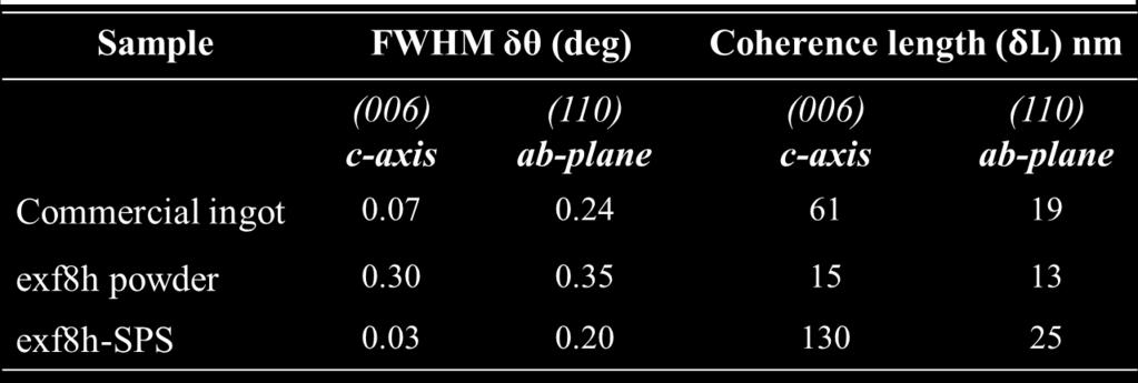
1 Supplementary Information for Preferential Scattering by Interfacial Charged Defects for Enhanced Thermoelectric Performance in Few-layered n-type Bi 2 Te 3 Pooja Puneet, 1 Ramakrishna Podila, 1,2 Mehmet Karakaya, 1 Song Zhu, 1 Jian He, 1,* Terry M. Tritt, 1 Mildred S. Dresselhaus, 3 and Apparao M. Rao 1,2,* Affiliations: 1. Department of Physics and Astronomy, Clemson University, Clemson, South Carolina, SC USA 2. Center for Optical Materials Science and Engineering Technologies, Clemson University, Clemson, SC USA 3. Department of Physics and Electrical Engineering, Massachusetts Institute of Technology, Cambridge, Massachusetts 02139, USA Correspondence to: arao@g.clemson.edu and jianhe@clemson.edu X-ray diffraction- All samples used in this study exhibited a x-ray diffraction (XRD) pattern (Fig. S1) that was consistent with single phase of Bi 2 Te 2.7 Se 0.3 (JCPDS card no ). Pristine Bi 2 Te 3 exhibits!3! symmetry but it is often more convenient to view the structure as a hexagonal crystallographic unit cell. The crystallographic unit cell of Bi 2 Te 3 is shown in Fig. S2 with the basal plane and c-axis directions. As expected, we found that the full width at half maximum intensity (FWHM) (!") (0,0,6) peak broadened due to the formation of few-layer nanosheets. The FWHM was obtained after subtracting the instrumental broadening. We estimated the coherence length (δl) for our samples along the in-plane [00l] and cross-plane [hk0] directions from the XRD data using Equation 1: 1
 direction. Figure S1: (a) Powder x-ray diffraction patterns of the commercial ingot, exf8h and exf8h-sps samples (see text).")
2 !" =!!!", (Eq. 1)!h!"!!" =!!!!"#$.!". As shown in Table S1, the average values for δl showed a significant increase for the exf8h-sps sample along the (0,0,6) direction while!" did not change significantly along the (1,1,0) direction. Figure S1: (a) Powder x-ray diffraction patterns of the commercial ingot, exf8h and exf8h-sps samples (see text). In panels (b) and (c) the (0,0,6) peak is suppressed in exf8h samples due to exfoliation, whereas more pronounced (0,0,6) and (1,1,0) peaks are evident in the exf8h-sps sample indicating the improvement in coherence length. Table S1: FWHM and coherence length calculated from powder XRD data. 2
3 3


4 Figure S2: Hexagonal crystallographic unit cell of Bi 2 Te 3. The indices represent the bonding environment of Te atoms. Te 1 represents van der Waal bonding whereas Te 2 represents ioniccovalent type of bonding with Bi atoms. 4
 and resistivity (ρ) in order to obtain correct ZT values.")
 can result in a higher but inaccurate ZT. To ensure the uniformity in measurements, we adhered to a protocol we developed previously Ref.")
5 Thermal conductivity- The thermal conductivity (κ) measurements are very critical in the determination of ZT. It is important to measure κ in the same direction as thermopower (α) and resistivity (ρ) in order to obtain correct ZT values. Particularly, in case of Bi 2 Te 3, the high anisotropy can result in miscalculated ZT values. As shown in Fig. S3, measuring κ along the SPS direction (open squares) can result in a higher but inaccurate ZT. To ensure the uniformity in measurements, we adhered to a protocol we developed previously Ref. 21 for measuring κ in the same direction as ρ and α. Figure S3: Anisotropy in the transport measurements along SPS direction (open symbols) and normal to SPS direction (solid symbols) directions is shown in (a). Electrical transport properties are measured in the direction normal to SPS direction and high temperature κ is measured in SPS direction of the pellet; the effect of anisotropy on the κ Total (b) and ZT values (c) of exf8h samples is shown. 5
, electronic (κ e ), and bipolar (κ B ) to the total thermal conductivity")
 and the")

6 Figure S4: Separation of various contributing thermal conductivities: lattice (κ L ), electronic (κ e ), and bipolar (κ B ) to the total thermal conductivity (κ T ) are shown for the commercial n-type Bi 2 Te 3 ingot. The solid symbols represent data for total thermal conductivity (κ T ) and the open symbols represent (κ T- κ e ). Table S2: Contributions from lattice, electronic and bipolar thermal conductivities to the total thermal conductivity κ T at 300 K and 450 K. 6


7 Figure S5: The bipolar thermal conductivity (κ B ) was estimated from κ T as explained earlier in the results and discussions section. The temperature dependence of bipolar thermal conductivity (κ B ) shows a shift in the onset for bipolar contributions to higher temperature for the exf8h-sps samples. The contribution of κ B below the onset T is close to zero. A corresponding shift in the ZT peak position confirmed that the shift in bipolar effects resulted in higher ZT values at high temperatures. 7
8 Effects of exfoliation time- To elucidate the effects of exfoliation time, we exfoliated bulk n- type Bi 2 Te 3 for 3, 5, and 8h. As shown in Fig. S6, we observed a weak influence of exfoliation time on the TE properties of CE-SPS processed n-type Bi 2 Te 3. Furthermore, AFM measurements (Fig. S7) showed that the thickness of exfoliated samples does not vary for exfoliations times greater than 3h, consistent the trends observed in TE properties. Figure S6: The effect of exfoliation time (followed by a SPS treatment) on the transport properties: α (a), ρ (b) and the power factor α 2 T/ρ (c) as a function of temperature. 8
9 Figure S7: The average thickness of exfoliated n-type Bi 2 Te 3 decreases rapidly with increasing exfoliation time (from 0 to 3 h, and 3 to 5 h) and eventually plateaus at ~50 nm when exfoliation time exceeds 8 h. The inset shows the change in the intensity of the 760 cm -1 Raman peak (cf. Fig. 5) as a function of exfoliation time. It is evident that the saturation in the Raman peak intensity correlates with the observed lack of change in the layer thickness at extended exfoliation times. 9
SUPPLEMENTARY INFORMATION
 Supplementary Methods Materials Synthesis The In 4 Se 3-δ crystal ingots were grown by the Bridgeman method. The In and Se elements were placed in an evacuated quartz ampoule with an excess of In (5-10
Supporting Information
 Supporting Information Cellulose Fiber-based Hierarchical Porous Bismuth Telluride for High-Performance Flexible and Tailorable Thermoelectrics Qun Jin a,b, Wenbo Shi c,d, Yang Zhao a,c, Jixiang Qiao a,c,
Synthesis and Characterization of Exfoliated Graphite (EG) and to Use it as a Reinforcement in Zn-based Metal Matrix Composites
 and to Use it as a Reinforcement in Zn-based Metal Matrix Composites") Synthesis and Characterization of Exfoliated Graphite (EG) and to Use it as a Reinforcement in Zn-based Metal Matrix Composites Here H 2 SO 4 was used as an intercalant and H 2 O 2 as an oxidant. Expandable
Synthesis and Characterization of Exfoliated Graphite (EG) and to Use it as a Reinforcement in Zn-based Metal Matrix Composites Here H 2 SO 4 was used as an intercalant and H 2 O 2 as an oxidant. Expandable
Supporting Information
 Copyright WILEY-VCH Verlag GmbH & Co. KGaA, 69469 Weinheim, Germany, 2015. Supporting Information for Adv. Mater., DOI: 10.1002/adma.201502134 Stable Metallic 1T-WS 2 Nanoribbons Intercalated with Ammonia
Supporting Information
 Supporting Information Enhanced thermoelectricity in High-temperature β-phase Copper (I) Selenides embedded with Cu 2 Te nanoclusters Sajid Butt, a,b, * Wei Xu, c,f, * Muhammad U. Farooq, d Guang K. Ren,
Supplementary Figure 1 Characterization of the synthesized BP crystal (a) Optical microscopic image of bulk BP (scale bar: 100 μm).
 Optical microscopic image of bulk BP (scale bar: 100 μm).") Supplementary Figure 1 Characterization of the synthesized BP crystal (a) Optical microscopic image of bulk BP (scale bar: 100 μm). Inset shows as-grown bulk BP specimen (scale bar: 5 mm). (b) Unit cell
Supplementary Figure 1 Characterization of the synthesized BP crystal (a) Optical microscopic image of bulk BP (scale bar: 100 μm). Inset shows as-grown bulk BP specimen (scale bar: 5 mm). (b) Unit cell
a b c Supplementary Figure S1
 a b c Supplementary Figure S1 AFM measurements of MoS 2 nanosheets prepared from the electrochemical Liintercalation and exfoliation. (a) AFM measurement of a typical MoS 2 nanosheet, deposited on Si/SiO
Supplementary Figure S1: Number of Fermi surfaces. Electronic dispersion around Γ a = 0 and Γ b = π/a. In (a) the number of Fermi surfaces is even,
 the number of Fermi surfaces is even,") Supplementary Figure S1: Number of Fermi surfaces. Electronic dispersion around Γ a = 0 and Γ b = π/a. In (a) the number of Fermi surfaces is even, whereas in (b) it is odd. An odd number of non-degenerate
Supplementary Figure S1: Number of Fermi surfaces. Electronic dispersion around Γ a = 0 and Γ b = π/a. In (a) the number of Fermi surfaces is even, whereas in (b) it is odd. An odd number of non-degenerate
Anisotropy in Thermoelectric Properties of CsBi 4 Te 6
 Mat. Res. Soc. Symp. Proc. Vol. 793 24 Materials Research Society S6.1.1 Anisotropy in Thermoelectric Properties of CsBi 4 Te 6 Duck-Young Chung 1, S. D. Mahanti 2, Wei Chen 3, Citrad Uher 3, Mercouri
Thickness-Dependent and Magnetic- Field-Driven Suppression of Antiferromagnetic Order in Thin V5S8 Single Crystals
 Supporting Information for: Thickness-Dependent and Magnetic- Field-Driven Suppression of Antiferromagnetic Order in Thin V5S8 Single Crystals Will J. Hardy, # Jiangtan Yuan, # Hua Guo, Panpan Zhou, Jun
CHAPTER 3. OPTICAL STUDIES ON SnS NANOPARTICLES
 42 CHAPTER 3 OPTICAL STUDIES ON SnS NANOPARTICLES 3.1 INTRODUCTION In recent years, considerable interest has been shown on semiconducting nanostructures owing to their enhanced optical and electrical
Rotational symmetry breaking in the topological superconductor SrxBi2Se3 probed by uppercritical
 UvA-DARE (Digital Academic Repository) Rotational symmetry breaking in the topological superconductor SrxBi2Se3 probed by uppercritical field experiments Pan, Y.; Nikitin, A.; Araizi Kanoutas, G.; Huang,
Supplementary Materials for
 advances.sciencemag.org/cgi/content/full/2/1/e151117/dc1 Supplementary Materials for Quantum Hall effect in a bulk antiferromagnet EuMni2 with magnetically confined two-dimensional Dirac fermions Hidetoshi
Thermoelectric Oxide Materials For Electric Power Generation
 Thermoelectric Oxide Materials For Electric Power Generation Kunihito Koumoto Nagoya University, Graduate School of Engineering CREST, Japan Science and Technology Agency 1. Thermoelectric Energy Conversion
SUPPLEMENTARY NOTE 1: ANISOTROPIC MAGNETORESISTANCE PHE-
 SUPPLEMENTARY NOTE 1: ANISOTROPIC MAGNETORESISTANCE PHE- NOMENOLOGY In the main text we introduce anisotropic magnetoresistance (AMR) in analogy to ferromagnets where non-crystalline and crystalline contributions
Supplementary Information. for. Controlled Scalable Synthesis of Uniform, High-Quality Monolayer and Fewlayer
 Supplementary Information for Controlled Scalable Synthesis of Uniform, High-Quality Monolayer and Fewlayer MoS 2 Films Yifei Yu 1, Chun Li 1, Yi Liu 3, Liqin Su 4, Yong Zhang 4, Linyou Cao 1,2 * 1 Department
SUPPLEMENTARY INFORMATION. Lamuel David, Romil Bhandavat and Gurpreet Singh*
 SUPPLEMENTARY INFORMATION MoS 2 /graphene Composite Paper For Sodium-Ion Battery Electrodes Lamuel David, Romil Bhandavat and Gurpreet Singh* Mechanical and Nuclear Engineering Department, Kansas State
Supplementary for Disorder Dependent Valley Properties in Monolayer WSe 2
 Supplementary for Disorder Dependent Valley Properties in Monolayer WSe 2 Kha Tran 1, Akshay Singh 1,*, Joe Seifert 1, Yiping Wang 1, Kai Hao 1, Jing-Kai Huang 2, Lain-Jong Li 2, Takashi Taniguchi 4, Kenji
Tunable Dirac Fermion Dynamics in Topological Insulators
 Supplementary information for Tunable Dirac Fermion Dynamics in Topological Insulators Chaoyu Chen 1, Zhuojin Xie 1, Ya Feng 1, Hemian Yi 1, Aiji Liang 1, Shaolong He 1, Daixiang Mou 1, Junfeng He 1, Yingying
Semester Length Glass Courses and Glass Schools
 Lehigh University Lehigh Preserve US-Japan Winter School Semester Length Glass Courses and Glass Schools Winter 1-1-2008 Special lecture, Part 1: Nature-guided nanotechnology for chemical tectonics of
Arnab Pariari & Prabhat Mandal Saha Institute of Nuclear Physics, 1/AF Bidhannagar, Calcutta , India
 Supplementary information for Coexistence of topological Dirac fermions on the surface and three-dimensional Dirac cone state in the bulk of ZrTe 5 single crystal Arnab Pariari & Prabhat Mandal Saha Institute
Supplementary Figure 1: Spin noise spectra of 55 Mn in bulk sample at BL =10.5 mt, before subtraction of the zero-frequency line. a, Contour plot of
 1 Supplementary Figure 1: Spin noise spectra of 55 Mn in bulk sample at BL =10.5 mt, before subtraction of the zero-frequency line. a, Contour plot of the spin noise spectra calculated with Eq. (2) for
Supplementary Figures
 Supplementary Figures Supplementary Figure 1: Region mapping. a Pristine and b Mn-doped Bi 2 Te 3. Arrows point at characteristic defects present on the pristine surface which have been used as markers
Supplementary Information
 Supplementary Information Supplementary Figure S1: Structure and composition of Teflon tape. (a) XRD spectra of original Teflon tape and Teflon tape subjected to annealing at 150 o C under Ar atmosphere.
Supplementary Figures
 Supplementary Figures Supplementary Figure 1 Measured versus calculated optical transitions in the CPX. The UV/Vis/NIR spectrum obtained experimentally for the 1:1 blend of 4T and F4TCNQ (red curve) is
Observation of topological surface state quantum Hall effect in an intrinsic three-dimensional topological insulator
 Observation of topological surface state quantum Hall effect in an intrinsic three-dimensional topological insulator Authors: Yang Xu 1,2, Ireneusz Miotkowski 1, Chang Liu 3,4, Jifa Tian 1,2, Hyoungdo
Intensity (a.u.) 2Theta (degrees) Supplementary data O 3 BO 3. Sup-Figure 1: Room temperature XRD patterns of KCaBO 3 :Eu 3+ sample treated at 500 ºC.
 2Theta (degrees) Supplementary data O 3 BO 3. Sup-Figure 1: Room temperature XRD patterns of KCaBO 3 :Eu 3+ sample treated at 500 ºC.") Supplementary data The following results and discussions are for the low-temperature (5 C) processed phosphors. 5 ºC Intensity (a.u.) KCaBO 3 Eu 2 O 3 H 3 BO 3 2 3 4 5 2Theta (degrees) 6 7 Sup-Figure 1:
Supplementary data The following results and discussions are for the low-temperature (5 C) processed phosphors. 5 ºC Intensity (a.u.) KCaBO 3 Eu 2 O 3 H 3 BO 3 2 3 4 5 2Theta (degrees) 6 7 Sup-Figure 1:
performance electrocatalytic or electrochemical devices. Nanocrystals grown on graphene could have
 Nanocrystal Growth on Graphene with Various Degrees of Oxidation Hailiang Wang, Joshua Tucker Robinson, Georgi Diankov, and Hongjie Dai * Department of Chemistry and Laboratory for Advanced Materials,
Thermal conductivity: An example of structure-property relations in crystals Ram Seshadri
 Thermal conductivity: An example of structure-property relations in crystals Ram Seshadri Materials Department, and Department of Chemistry and Biochemistry Materials Research Laboratory University of
Anisotropic thermoelectric properties of layered compound In 2 Te 5 single crystal
 1 Anisotropic thermoelectric properties of layered compound In 2 Te 5 single crystal Anup V. Sanchela, Ajay D. Thakur,, C. V. Tomy a Department of Physics, Indian Institute of Technology Bombay, Powai,
SUPPLEMENTARY INFORMATION
 SUPPLEMENTARY INFORMATION I. Experimental Thermal Conductivity Data Extraction Mechanically exfoliated graphene flakes come in different shape and sizes. In order to measure thermal conductivity of the
unique electronic structure for efficient hydrogen evolution
 Electronic Supplementary Material (ESI) for Journal of Materials Chemistry A. This journal is The Royal Society of Chemistry 2017 Supplementary Information Atom-scale dispersed palladium in conductive
Electronic Supplementary Information
 Electronic Supplementary Material (ESI) for Journal of Materials Chemistry A. This journal is The Royal Society of Chemistry 2016 Electronic Supplementary Material (ESI) for Journal of Materials Chemistry
YBCO. CuO 2. the CuO 2. planes is controlled. from deviation from. neutron. , blue star for. Hg12011 (this work) for T c = 72
 for T c = 72") Supplementary Figure 1 Crystal structures and joint phase diagram of Hg1201 and YBCO. (a) Hg1201 features tetragonal symmetry and one CuO 2 plane per primitive cell. In the superconducting (SC) doping
Supplementary Figure 1 Crystal structures and joint phase diagram of Hg1201 and YBCO. (a) Hg1201 features tetragonal symmetry and one CuO 2 plane per primitive cell. In the superconducting (SC) doping
Supplementary Information: Supplementary Figure 1. Resistance dependence on pressure in the semiconducting region.
 Supplementary Information: Supplementary Figure 1. Resistance dependence on pressure in the semiconducting region. The pressure activated carrier transport model shows good agreement with the experimental
Supplementary information
 Supplementary information Preparation of Few-Layer Bismuth Selenide by Liquid-Phase-Exfoliation and Its Optical Absorption Properties Liping Sun 1, Zhiqin Lin 1, Jian Peng 1, Jian Weng 1,3 *, Yizhong Huang
STUDIES ON ZnS - CuS NANOPARTICLE SYSTEM.
 CHAPTER - VI STUDIES ON ZnS - CuS NANOPARTICLE SYSTEM. 6.1 INTRODUCTION ZnS is an important direct band gap semiconductor. It has a band gap energy of 3.6 ev[1], displays a high refractive index (2.37)
Phases of Na x CoO 2
 Phases of Na x CoO 2 by Aakash Pushp (pushp@uiuc.edu) Abstract This paper deals with the various phases of Na x CoO 2 ranging from charge ordered insulator to Curie-Weiss metal to superconductor as the
SUPPLEMENTARY INFORMATION
 In the format provided by the authors and unedited. SUPPLEMENTARY INFORMATION DOI: 10.1038/NPHOTON.017.65 Imaging exciton-polariton transport in MoSe waveguides F. Hu 1,, Y. Luan 1,, M. E. Scott 3, J.
Supporting Information Inherent Electrochemistry and Charge Transfer Properties of Few-Layer Two Dimensional Ti 3 C 2 T x MXene
 Electronic Supplementary Material (ESI) for Nanoscale. This journal is The Royal Society of Chemistry 2018 Supporting Information Inherent Electrochemistry and Charge Transfer Properties of Few-Layer Two
Supplementary Figure S1. AFM characterizations and topographical defects of h- BN films on silica substrates. (a) (c) show the AFM height
 (c) show the AFM height") Supplementary Figure S1. AFM characterizations and topographical defects of h- BN films on silica substrates. (a) (c) show the AFM height topographies of h-bn film in a size of ~1.5µm 1.5µm, 30µm 30µm
Supplementary Figure S1. AFM characterizations and topographical defects of h- BN films on silica substrates. (a) (c) show the AFM height topographies of h-bn film in a size of ~1.5µm 1.5µm, 30µm 30µm
Supplementary file XRD. Supplementary figure 1. XRD pattern of pristine Co 3 O 4 and higher dopant (Ag 0.5 Co 2.5 O 4 biphasic).
.") Electronic Supplementary Material (ESI) for Catalysis Science & Technology. This journal is The Royal Society of Chemistry 2015 Supplementary file Preparation of CO and NO The CO was prepared by disproportionation
Electronic Supplementary Material (ESI) for Catalysis Science & Technology. This journal is The Royal Society of Chemistry 2015 Supplementary file Preparation of CO and NO The CO was prepared by disproportionation
Valleytronics, Carrier Filtering and Thermoelectricity in Bismuth: Magnetic Field Polarization Effects
 Valleytronics, Carrier Filtering and Thermoelectricity in Bismuth: Magnetic Field Polarization Effects Adrian Popescu and Lilia M. Woods * Valley polarization of multi-valleyed materials is of significant
Structural phase transitions in Bi 2 Se 3 under high pressure
 Structural phase transitions in Bi 2 Se 3 under high pressure Zhenhai Yu 1, Lin Wang 1,2,7 * Qingyang Hu 1,7, Jinggeng Zhao 3, Shuai Yan 4, Ke Yang 4, Stanislav Sinogeikin 5, Genda Gu 6 & Ho-kwang Mao
Supporting Information Available:
 Supporting Information Available: Photoresponsive and Gas Sensing Field-Effect Transistors based on Multilayer WS 2 Nanoflakes Nengjie Huo 1, Shengxue Yang 1, Zhongming Wei 2, Shu-Shen Li 1, Jian-Bai Xia
Structure, crystal fields, magnetic interactions, and heavy-fermion behavior in Ce 1 x La x 3 Al
 PHYSICAL REVIEW B VOLUME 55, NUMBER 9 1 MARCH 1997-I Structure, crystal fields, magnetic interactions, and heavy-fermion behavior in Ce 1 x La x 3 Al Y. Y. Chen and Y. D. Yao Institute of Physics, Academia
Supplementary Figures
 Supplementary Figures Supplementary Figure 1: Microstructure, morphology and chemical composition of the carbon microspheres: (a) A SEM image of the CM-NFs; and EDS spectra of CM-NFs (b), CM-Ns (d) and
Observation of quadrupole helix chirality and its domain structure in DyFe 3 (BO 3 ) 4
 4") Observation of quadrupole helix chirality and its domain structure in DyFe 3 (BO 3 ) 4 T. Usui, Y. Tanaka, H. Nakajima, M. Taguchi, A. Chainani, M. Oura, S. Shin, N. Katayama, H. Sawa, Y. Wakabayashi,
Observation of quadrupole helix chirality and its domain structure in DyFe 3 (BO 3 ) 4 T. Usui, Y. Tanaka, H. Nakajima, M. Taguchi, A. Chainani, M. Oura, S. Shin, N. Katayama, H. Sawa, Y. Wakabayashi,
Supplementary Figures:
 Supplementary Figures: dcdtbt vibration spectrum: Ground state blue vs Cation state red Intensity a.u. 1000 1100 1200 1300 1400 1500 1600 1700 Frequency cm^1 dcdtbt vibration spectrum: Ground state blue
Bandgap engineering through nanocrystalline magnetic alloy grafting on. graphene
 Electronic Supplementary Material (ESI) for Physical Chemistry Chemical Physics. This journal is the Owner Societies 2014 Electronic Supplementary Information (ESI) for Bandgap engineering through nanocrystalline
Supplementary Figures
 Supplementary Figures Supplementary Figure 1. Crystal structure of 1T -MoTe 2. (a) HAADF-STEM image of 1T -MoTe 2, looking down the [001] zone (scale bar, 0.5 nm). The area indicated by the red rectangle
SUPPLEMENTARY INFORMATION
 Lateral heterojunctions within monolayer MoSe 2 -WSe 2 semiconductors Chunming Huang 1,#,*, Sanfeng Wu 1,#,*, Ana M. Sanchez 2,#,*, Jonathan J. P. Peters 2, Richard Beanland 2, Jason S. Ross 3, Pasqual
Supplementary Figure 1 Scheme image of GIXD set-up. The scheme image of slot die
 Supplementary Figure 1 Scheme image of GIXD set-up. The scheme image of slot die printing system combined with grazing incidence X-ray diffraction (GIXD) set-up. 1 Supplementary Figure 2 2D GIXD images
Charge Transport and Thermoelectric Properties of P-type Bi 2-x Sb x Te 3 Prepared by Mechanical Alloying and Hot Pressing
 [Research Paper] 대한금속 재료학회지 (Korean J. Met. Mater.), Vol. 56, No. 1 (2018), pp.66-71 66 DOI: 10.3365/KJMM.2018.56.1.66 Charge Transport and Thermoelectric Properties of P-type Bi 2-x Sb x Te 3 Prepared
Supporting information for
 Supporting information for Metallic Few-layered VS 2 Ultrathin Nanosheets: High Two-Dimensional Conductivity for In-Plane Supercapacitors Jun Feng, Xu Sun, Changzheng Wu*, Lele Peng, Chenwen Lin, Shuanglin
SUPPLEMENTARY INFORMATION
 DOI: 1.138/NMAT3449 Topological crystalline insulator states in Pb 1 x Sn x Se Content S1 Crystal growth, structural and chemical characterization. S2 Angle-resolved photoemission measurements at various
SUPPLEMENTARY INFORMATION
 SUPPLEMENTARY INFORMATION Facile Synthesis of High Quality Graphene Nanoribbons Liying Jiao, Xinran Wang, Georgi Diankov, Hailiang Wang & Hongjie Dai* Supplementary Information 1. Photograph of graphene
Reduced Lattice Thermal Conductivity in Bi-doped Mg 2 Si 0.4 Sn 0.6
 Reduced Lattice Thermal Conductivity in Bi-doped Mg 2 Si 0.4 Sn 0.6 Peng Gao 1, Xu Lu 2, Isil Berkun 3, Robert D. Schmidt 1, Eldon D. Case 1 and Timothy P. Hogan 1,3 1. Department of Chemical Engineering
The Effects of Nanoparticle Inclusions upon the Microstructure and Thermoelectric Transport Properties of Bismuth Telluride-Based Composites
 Clemson University TigerPrints All Dissertations Dissertations 8-2008 The Effects of Nanoparticle Inclusions upon the Microstructure and Thermoelectric Transport Properties of Bismuth Telluride-Based Composites
Supporting information Chemical Design and Example of Transparent Bipolar Semiconductors
 Supporting information Chemical Design and Example of Transparent Bipolar Semiconductors Takeshi Arai 1, Soshi Iimura 1, *, Junghwan Kim 2, Yoshitake Toda 2, Shigenori Ueda 3, 4, and Hideo Hosono 1, 2,
High-Performance Flexible Asymmetric Supercapacitors Based on 3D. Electrodes
 Supporting Information for: High-Performance Flexible Asymmetric Supercapacitors Based on 3D Porous Graphene/MnO 2 Nanorod and Graphene/Ag Hybrid Thin-Film Electrodes Yuanlong Shao, a Hongzhi Wang,* a
C. C. WILSON. ISIS Facility, Rutherford Appleton Laboratory, Chilton, Didcot, Oxon OX 11 OQX, UK
 Structural studies of schultenite in the temperature range 125-324 K by pulsed single crystal neutron diffraction- hydrogen ordering and structural distortions C. C. WILSON ISIS Facility, Rutherford Appleton
Theoretical investigation of thermoelectric transport properties of cylindrical Bi nanowires
 PHYSICAL REVIEW B VOLUME 6, NUMBER 7 15 AUGUST 000-I Theoretical investigation of thermoelectric transport properties of cylindrical Bi nanowires Yu-Ming Lin, 1 Xiangzhong Sun, and M. S. Dresselhaus 1,
Superconductivity and non-metallicity induced by doping the. topological insulators Bi 2 Se 3 and Bi 2 Te 3
 Superconductivity and non-metallicity induced by doping the topological insulators Bi 2 Se 3 and Bi 2 Te 3 Y. S. Hor 1, J. G. Checkelsky 2, D. Qu 2, N. P. Ong 2, and R. J. Cava 1 1 Department of Chemistry,
Harald Ibach Hans Lüth SOLID-STATE PHYSICS. An Introduction to Theory and Experiment
 Harald Ibach Hans Lüth SOLID-STATE PHYSICS An Introduction to Theory and Experiment With 230 Figures Springer-Verlag Berlin Heidelberg New York London Paris Tokyo Hong Kong Barcelona Budapest Contents
Supporting Information
 Supporting Information Extraordinary Off-stoichiometric Bismuth Telluride for Enhanced n- type Thermoelectric Power Factor Kunsu Park,,,# Kyunghan Ahn,,# Joonil Cha,, Sanghwa Lee,, Sue In Chae,, Sung-
Supplementary Figure 1: Micromechanical cleavage of graphene on oxygen plasma treated Si/SiO2. Supplementary Figure 2: Comparison of hbn yield.
 1 2 3 4 Supplementary Figure 1: Micromechanical cleavage of graphene on oxygen plasma treated Si/SiO 2. Optical microscopy images of three examples of large single layer graphene flakes cleaved on a single
Supporting Information: A comparative Electron Paramagnetic Resonance study of expanded graphites and graphene
 Electronic Supplementary Material (ESI) for Journal of Materials Chemistry C. This journal is The Royal Society of Chemistry 2014 Supporting Information: A comparative Electron Paramagnetic Resonance study
M2 TP. Low-Energy Electron Diffraction (LEED)
") M2 TP Low-Energy Electron Diffraction (LEED) Guide for report preparation I. Introduction: Elastic scattering or diffraction of electrons is the standard technique in surface science for obtaining structural
M2 TP Low-Energy Electron Diffraction (LEED) Guide for report preparation I. Introduction: Elastic scattering or diffraction of electrons is the standard technique in surface science for obtaining structural
Transport properties of composition tuned - and -Eu 8 Ga 16 x Ge 30+x
 Transport properties of composition tuned - and -Eu 8 Ga 16 x Ge 30+x A. Bentien, V. Pacheco,* S. Paschen, Yu. Grin, and F. Steglich Max Planck Institute for Chemical Physics of Solids, Nöthnitzer Str.
Half Heusler Alloys for Efficient Thermoelectric Power Conversion
 Half Heusler Alloys for Efficient Thermoelectric Power Conversion L. Chen, 1,a) X. Zeng, T. M. Tritt,,3 and S. J. Poon 1,a) 1 Department of Physics, University of Virginia, Charlottesville, Virginia 904-4714
Supplementary Information for Optical and magneto-optical behavior of Cerium Yttrium Iron Garnet thin films at wavelengths of nm
 Supplementary Information for Optical and magneto-optical behavior of Cerium Yttrium Iron Garnet thin films at wavelengths of 200-1770 nm Mehmet C. Onbasli 1,a), Lukáš Beran 2,a), Martin Zahradník 2, Miroslav
Lithium Ion Insertion Properties of Solution-Exfoliated Germanane
 Lithium Ion Insertion Properties of Solution-Exfoliated Germanane Andrew C. Serino, Jesse S. Ko, Michael T. Yeung, Jeffrey J. Schwartz, Chris B. Kang, Sarah H. Tolbert,,, Richard B. Kaner,,, Bruce S. Dunn,*,,
Supplementary Information: Triggered self-assembly of magnetic nanoparticles
 Supplementary Information: Triggered self-assembly of magnetic nanoparticles L. Ye 1,3, T. Pearson 1, Y. Cordeau 2, O.T. Mefford 2, and T. M. Crawford 1 1 Smart State Center for Experimental Nanoscale
SUPPLEMENTARY MATERIALS FOR PHONON TRANSMISSION COEFFICIENTS AT SOLID INTERFACES
 148 A p p e n d i x D SUPPLEMENTARY MATERIALS FOR PHONON TRANSMISSION COEFFICIENTS AT SOLID INTERFACES D.1 Overview The supplementary information contains additional information on our computational approach
Thermoelectric Properties and Electrical Transport of Graphite Intercalation Compounds
 Materials Transactions, Vol. 5, No. 7 (9) pp. 167 to 1611 Special Issue on Thermoelectric Conversion Materials V #9 The Thermoelectrics Society of Japan Thermoelectric Properties and Electrical Transport
sgsp agsp W=20nm W=50nm Re(n eff (e) } Re{E z Im{E x Supplementary Figure 1: Gap surface plasmon modes in MIM waveguides.
 } Re{E z Im{E x Supplementary Figure 1: Gap surface plasmon modes in MIM waveguides.") (a) 2.4 (b) (c) W Au y Electric field (a.u) x SiO 2 (d) y Au sgsp x Energy (ev) 2. 1.6 agsp W=5nm W=5nm 1.2 1 2 3 4.1.1 1 1 Re(n eff ) -1-5 5 1 x (nm) W = 2nm E = 2eV Im{E x } Re{E z } sgsp Electric field
(a) 2.4 (b) (c) W Au y Electric field (a.u) x SiO 2 (d) y Au sgsp x Energy (ev) 2. 1.6 agsp W=5nm W=5nm 1.2 1 2 3 4.1.1 1 1 Re(n eff ) -1-5 5 1 x (nm) W = 2nm E = 2eV Im{E x } Re{E z } sgsp Electric field
A. Optimizing the growth conditions of large-scale graphene films
 1 A. Optimizing the growth conditions of large-scale graphene films Figure S1. Optical microscope images of graphene films transferred on 300 nm SiO 2 /Si substrates. a, Images of the graphene films grown
disordered, ordered and coherent with the substrate, and ordered but incoherent with the substrate.
 5. Nomenclature of overlayer structures Thus far, we have been discussing an ideal surface, which is in effect the structure of the topmost substrate layer. The surface (selvedge) layers of the solid however
Current-induced switching in a magnetic insulator
 In the format provided by the authors and unedited. DOI: 10.1038/NMAT4812 Current-induced switching in a magnetic insulator Can Onur Avci, Andy Quindeau, Chi-Feng Pai 1, Maxwell Mann, Lucas Caretta, Astera
Microporous carbon nanosheets with redox-active. heteroatoms for pseudocapacitive charge storage
 Electronic Supplementary Material (ESI) for Nanoscale. This journal is The Royal Society of Chemistry 2015 SUPPORTING INFORMATION Microporous carbon nanosheets with redox-active heteroatoms for pseudocapacitive
Supporting Information. Molecular Selectivity of. Graphene-Enhanced Raman Scattering
 1 Supporting Information 2 3 4 5 6 7 8 9 10 11 12 13 14 15 16 17 18 19 20 21 22 23 24 25 Molecular Selectivity of Graphene-Enhanced Raman Scattering Shengxi Huang,, Xi Ling,,, * Liangbo Liang, ǁ Yi Song,
Intensity (a.u.) Intensity (a.u.) Raman Shift (cm -1 ) Oxygen plasma. 6 cm. 9 cm. 1mm. Single-layer graphene sheet. 10mm. 14 cm
 Intensity (a.u.) Raman Shift (cm -1 ) Oxygen plasma. 6 cm. 9 cm. 1mm. Single-layer graphene sheet. 10mm. 14 cm") Intensity (a.u.) Intensity (a.u.) a Oxygen plasma b 6 cm 1mm 10mm Single-layer graphene sheet 14 cm 9 cm Flipped Si/SiO 2 Patterned chip Plasma-cleaned glass slides c d After 1 sec normal Oxygen plasma
Intensity (a.u.) Intensity (a.u.) a Oxygen plasma b 6 cm 1mm 10mm Single-layer graphene sheet 14 cm 9 cm Flipped Si/SiO 2 Patterned chip Plasma-cleaned glass slides c d After 1 sec normal Oxygen plasma
height trace of a 2L BN mechanically exfoliated on SiO 2 /Si with pre-fabricated micro-wells. Scale bar 2 µm.
 Supplementary Figure 1. Few-layer BN nanosheets. AFM image and the corresponding height trace of a 2L BN mechanically exfoliated on SiO 2 /Si with pre-fabricated micro-wells. Scale bar 2 µm. Supplementary
Transition of p-ton-type Conductivity in Mechanically Activated Bismuth Telluride
 Journal of ELECTRONIC MATERIALS, Vol. 47, No. 10, 2018 https://doi.org/10.1007/s11664-018-6469-1 Ó 2018 The Minerals, Metals & Materials Society Transition of p-ton-type Conductivity in Mechanically Activated
Hall and field-effect mobilities in few layered p -WSe2 field-effect transistors Current-Voltage characteristics and leakage voltage Figure S1
 Supplemental information to manuscript titled: Hall and field-effect mobilities in few layered p-wse 2 field-effect transistors by Nihar R. Pradhan 1, Daniel Rhodes 1, Shariar Memaran 1, Jean M. Poumirol
Supplementary Information for Observation of dynamic atom-atom correlation in liquid helium in real space
 3 4 5 6 7 8 9 0 3 4 5 6 7 8 9 0 Supplementary Information for Observation of dynamic atom-atom correlation in liquid helium in real space Supplementary Note : Total PDF The total (snap-shot) PDF is obtained
Microporous Carbon adsorbents with high CO 2 capacities for industrial applications
 Microporous Carbon adsorbents with high CO 2 capacities for industrial applications Santiago Builes, a,b Thomas Roussel,* b Camelia Matei Ghimbeu, c Julien Parmentier, c Roger Gadiou, c Cathie Vix-Guterl
International Journal of Scientific & Engineering Research, Volume 5, Issue 3, March-2014 ISSN
 156 Copper Nanoparticles: Green Synthesis Characterization Y.Suresh*1, S.Annapurna*2, G.Bhikshamaiah*3, A.K.Singh#4 Abstract Present work describes the synthesis nanoparticles using papaya extract as a
Analytical Methods for Materials
 Analytical Methods for Materials Laboratory Module # Crystal Structure Determination for Non-Cubic Crystals Suggested Reading 1. Y. Waseda, E. Matsubara, and K. Shinoda, X-ray Diffraction Crystallography,
Highly Efficient Flexible Solar Cells Based on Room-Temperature
 Electronic Supplementary Material (ESI) for Journal of Materials Chemistry A. This journal is The Royal Society of Chemistry Please do 2018 not adjust margins Supporting Information Highly Efficient Flexible
Tailoring exchange couplings in magnetic topological-insulator/antiferromagnet heterostructures
 Tailoring exchange couplings in magnetic topological-insulator/antiferromagnet heterostructures Qing Lin He 1 *, Xufeng Kou 1, Alexander J. Grutter 2, Gen Yin 1, Lei Pan 1, Xiaoyu Che 1, Yuxiang Liu 1,
Structure and Dynamics : An Atomic View of Materials
 Structure and Dynamics : An Atomic View of Materials MARTIN T. DOVE Department ofearth Sciences University of Cambridge OXFORD UNIVERSITY PRESS Contents 1 Introduction 1 1.1 Observations 1 1.1.1 Microscopic
Tailoring Electrical Contact Resistivity at Metal-Thermoelectric Interfaces Using a Molecular Nanolayer
 Tailoring Electrical Contact Resistivity at Metal-Thermoelectric Interfaces Using a Molecular Nanolayer Thomas J. Cardinal Graduate Student Department of Materials Science & Engineering Rensselaer Polytechnic
Supporting Information. Anisotropic Electron-Phonon Interactions in Angle- Resolved Raman Study of Strained Black
 Supporting Information Anisotropic Electron-Phonon Interactions in Angle- Resolved Raman Study of Strained Black Phosphorus Weinan Zhu,* 1 Liangbo Liang,* 2 Richard H. Roberts, 3 Jung-Fu Lin, 3,4 and Deji
Perovskite Solar Cells Powered Electrochromic Batteries for Smart. Windows
 Electronic Supplementary Material (ESI) for Materials Horizons. This journal is The Royal Society of Chemistry 2016 Supporting Information for Perovskite Solar Cells Powered Electrochromic Batteries for
Supporting Information
 Supporting Information Cu O 3 : a new magnetically frustrated honeycomb iridate Mykola Abramchuk, Cigdem Ozsoy-Keskinbora, Jason W. Krizan, Kenneth R. Metz, David C. Bell,, and Fazel Tafti, Physics Department,
Pre-yield non-affine fluctuations and a hidden critical point in strained crystals
 Supplementary Information for: Pre-yield non-affine fluctuations and a hidden critical point in strained crystals Tamoghna Das, a,b Saswati Ganguly, b Surajit Sengupta c and Madan Rao d a Collective Interactions
SUPPLEMENTARY INFORMATION
 SUPPLEMENTARY INFORMATION DOI: 10.1038/NNANO.2011.138 Graphene Nanoribbons with Smooth Edges as Quantum Wires Xinran Wang, Yijian Ouyang, Liying Jiao, Hailiang Wang, Liming Xie, Justin Wu, Jing Guo, and
THERMOELECTRIC PROPERTIES OF THE HALF-HEUSLER COMPOUND (Zr,Hf)(Ni,Pd)Sn ABSTRACT
(Ni,Pd)Sn ABSTRACT") THERMOELECTRIC PROPERTIES OF THE HALF-HEUSLER COMPOUND (Zr,Hf)(Ni,Pd)Sn V. M. Browning a, S. J. Poon b, T. M. Tritt c, A.L Pope c, S. Bhattacharya c, P. Volkov b, J. G. Song b, V. Ponnambalam b, A. C.
THERMOELECTRIC PROPERTIES OF THE HALF-HEUSLER COMPOUND (Zr,Hf)(Ni,Pd)Sn V. M. Browning a, S. J. Poon b, T. M. Tritt c, A.L Pope c, S. Bhattacharya c, P. Volkov b, J. G. Song b, V. Ponnambalam b, A. C.