Computer Engineering Department. CC 311- Computer Architecture. Chapter 4. The Processor: Datapath and Control. Single Cycle
|
|
|
- Kevin Noel Booker
- 6 years ago
- Views:
Transcription
1 Computer Engineering Department CC 311- Computer Architecture Chapter 4 The Processor: Datapath and Control Single Cycle
2 Introduction The 5 classic components of a computer Processor Input Control Memory Datapath Output Chapter 4 discusses the processor Part-a: Datapath Part-b: Control 2
3 Review: Edge-triggered Methodology Input: Values written in a previous clock cycle Output: Values to be used in the following clock cycle Prevents reading the signal in the same time it is written More than one action can take place in the same clock cycle Falling edge Clock period Rising edge 3
4 Review: Timing Methodology Clock cycle(tick/period): Time for one clock period, usually of the processor, which runs at a constant rate Memory Access time: Time between the initiation of a read request and when the desired word arrives Memory Cycle time: Minimum time between requests to memory Should be greater than access time to keep address line stable between accesses 4
5 Review: Timing Methodology Typical execution cycle: Read contents of some state elements, Send values through some combinational logic Write results to one or more state elements Clock period should cover all these activities All signals must propagate from state element1 to state element2 in the time of one clock cycle If the state element is not updated on every clock, an explicit write control signal is required, in which case the state element is changed only when the control signal is asserted and the clock edge occurs 5
6 Review: Timing Methodology Edge triggered methodology allows a state element to be read and written in the same clock cycle The clock must be long enough to allow the stability of input value before the active edge occurs 6
7 Building the Datapath 7
8 Review: 2 x 1 MUX MUX Operation: Selects one of the (A or B) inputs to be the output, based on a control (select) input (S) We need a 2x1 MUX The MUX has 3 inputs Equivalent C-Operation If (s == 0) C:= A; else C = B; A B 0 1 (s) Selector C 8
9 Universal ALU Symbolic representation: (Sometimes used to represent adders as well) Operation a 32 C in to LSB Zero Flag ALU 32 Result b 32 C out from MSB Overflow Flag 9
10 Building the Datapath The major components required to execute each class of MIPS instructions? A memory unit to store the instructions PC to store the address of the current instruction Adder to increment PC to address of next instruction 10
11 Building the Datapath How are these components connected? 11
12 Building the Datapath The major components required to execute R-Format instructions add, sub, and, or, slt Three register operands Two read ports to read two registers from register file One write port to write into one register Data lines 32-bit Register lines ALUOp 12
13 Review: Register File A set of 32 registers 5-inputs 2 read-ports to supply source register numbers 1 write-port to supply destination register number 1 Data bus 1 Register write enable control signal 2-outputs Data from register 1 Data from register 2 1-Control signal RegWrite No need to read-enable 13 Register Selectors Data Bus Read Reg1 Read Reg 2 Write Reg1 Read Data1 Register File Read Data2 Write Data Write Enable RegWrite Data Buses 13
14 Review: Reading from Register File Need to submit: Read register number 1 Register 0 Register # For N-registers we need: Register 1... Register n 2 Register n 1 M u x Read data 1 n x 1 MUX Read register number 2 M u x Read data
15 Review: Writing to Register File Need to submit: Write Register # Data Write control signal Register number n-to-2n decoder 0 1. C D C Register 0 To choose a register, use Decoder To determine when to write, use the clock n 1 n D C Register 1. Note: C means control signal D C Register n 2 D means data lines Register data D Register n 1 15
16 Building the Datapath (lw, sw) Instruction Read register 1 Read Read data 1 register 2 Registers Read Write data 2 register Write data RegWrite ALUSrc M ux 3 ALU operation Zero ALU ALU result Address Write data MemWrite MemtoReg Data memory Read data M ux 16 Sign 32 extend MemRead 16
17 Building the Datapath (beq) For branch instructions, two operations are needed Compare register contents ALU Zero signal returns the result of comparison Compute branch target address A sign-extend unit is required If branch is taken Branch target address becomes the new PC contents If branch is not taken PC+4 is the new value for PC 17
18 Review: MIPS Instruction Format R-type op rs rt rd shamt funct 6 bits 5 bits 5 bits 5 bits 5 bits 6 bits 0 I-type op rs rt immediate 6 bits 5 bits 5 bits 16 bits 0 J-type op target address 6 bits 26 bits 0 18
19 Addressing Modes Register addressing Base or displacement addressing Immediate addressing PC-relative addressing Pseudo-direct addressing 19
20 Addressing Modes (1) Register addressing Operand is a register Value is the contents of the register 20
21 Building the Datapath R-type op rs rt rd shamt funct 6 bits 5 bits 5 bits 5 bits 5 bits 6 bits 0 21
22 Addressing Modes Register addressing Base or displacement addressing Immediate addressing PC-relative addressing Pseudo-direct addressing 22
23 Addressing Modes (2) Base or displacement addressing Operand location = register + constant (offset) in the instruction 23
24 Building the Datapath (sw) 24
25 Building the Datapath (lw) 25
26 Building Datapath (R-type, lw, sw) Instruction Read register 1 Read data 1 Read register 2 Registers Read Write data 2 register Write data RegWrite ALUSrc M u x 3 ALU ALU operation Zero ALU result Address Write data MemWrite MemtoReg Data memory Read data M u x 16 Sign 32 extend MemRead 26
27 Building Datapath (R-type, lw, sw) 27
28 Datapath Operation for R-Format (add) op rs rt rd shamt funct 6 bits 5 bits 5 bits 5 bits 5 bits 6 bits 0 Step1: Add $t1, $t2, $t3 Fetch instruction from instruction memory Increment program counter Step2: Decode result is Add operation Read two registers $t2 & $t3 from register file Step 3: ALU operates on data, using funct field code to generate the ALU function Step4: Write result of step 3 from ALU into register $t1 28
29 Datapath Operation for R-Format (add) Add $t1, $t2, $t3 (Fig. 5.19, p. 322) 29
30 Datapath Operation for R-Format (add) Step 1: Fetch instruction & increment PC 0 4 A d d I n s t r u c t i o n [ ] C o n t r o l R e g D s t B r a n c h M e m R e a d M e m t o R e g A L U O p M e m W r i t e A L U S r c R e g W r i t e S h i f t l e f t 2 A d d r e A s u L l U t M u x 1 P C R e a d a d d r e s s I n s t r u c t i o n m e m o r y I n s t r u c t i o n [ ] I n s t r u c t i o n [ ] I n s t r u c t i o n [ ] I n s t r u c t i o n [ 15 1 ] I n s t r u c t i o n [ 15 0 ] 0 M u x 1 R e a d r e g i s t e r 1 R e a d d a t a 1 i s t e r 2 R e g i s t e r s R e a d d a t a 2 R e a d r e g W r i t e r e g i s t e r W r i t e d a t a 16 S i g n 32 e x t e n d 0 M u x 1 A L U c o n t r o l Z e r o A L U A L U r e s u l t A d d r e s s W r i t e d a t a D a t a m e m o r y R e a d d a t a 1 M u x 0 I n s t r u c t i o n [ 5 0 ] 30
31 Datapath Operation for R-Format (add) Step2: Read registers from register file 4 A d d I n s t r u c t i o n [ ] C o n t r o l R e g D s t B r a n c h M e m R e a d M e m t o R e g A L U O p M e m W r i t e A L U S r c R e g W r i t e S h i f t l e f t 2 A d d r e A s u L l U t 0 M u x 1 P C R e a d a d d r e s s I n s t r u c t i o n m e m o r y I n s t r u c t i o n [ ] I n s t r u c t i o n [ ] I n s t r u c t i o n [ ] I n s t r u c t i o n [ ] I n s t r u c t i o n [ 15 0 ] 0 M u x 1 R e a d r e g i s t e r 1 R e a d R e a d d a t a 1 r e g i s t e r 2 i R e g i s t e r s R e a d W r i t e d a t a 2 r e g i s t e r i W r i t e d a t a S i g n e x t e n d 0 M u x 1 A L U c o n t r o l Z e r o A L U A L U r e s u l t A d d r e s s W r i t e d a t a D a t a m e m o r y R e a d d a t a 1 M u x 0 I n s t r u c t i o n [ 5 0 ] 31
32 Datapath Operation for R-Format (add) Step 3: Perform ALU operation 0 4 A d d I n s t r u c t i o n [ ] C o n t r o l R e g D s t B r a n c h M e m R e a d M e m t o R e g A L U O p M e m W r i t e A L U S r c R e g W r i t e S h i f t l e f t 2 A d d A L U r e s u t M u x 1 P C R e a d a d d r e s s I n s t r u c t o n m e m o r y I n s r u c t o n [ ] I n s t r u c t i o n [ ] I n s t r u c t i o n [ ] I n s t r u c t i o n [ 15 1 ] I n s t r u c t i o n [ 15 0 ] 0 M u x 1 R e a d r e g i s t e r 1 R e a d R e a d d a t a 1 r e g i s t e r 2 R e g i s t e r s R e a d W r i e d a t a 2 r e g i s t e r W r i e d a t a 16 S i g n 32 e x t e n d 0 M u x 1 A L U c o n t r o l Z e r o A L U A L U r e s u l t A d d r e s s W r i t e d a t a R e a d d a t a D a t a m e m o r y 1 M u x 0 I n s t r u c t i o n [ 5 0 ] 32
33 Datapath Operation for R-Format (add) Step 4: Write result from ALU into register 4 A d d I n s t r u c t i o n [ ] C o n t r o l R e g D s t B r a n c h M e m R e a d M e m t o R e g A L U O p M e m W r i t e A L U S r c R e g W r i t e S h i f t l e f t 2 A d d r e A s u L l U t 0 M u x 1 P C R e a d a d d r e s s I n s t r u c t i o n m e m o r y I n s t r u c t i o n [ ] I n s t r u c t i o n [ ] I n s t r u c t i o n [ ] I n s t r u c t i o n [ ] I n s t r u c t i o n [ 15 0 ] 0 M u x 1 R e a d r e g i s t e r 1 R e a d d a t a 1 i s t e r 2 R e g i s t e r s R e a d d a t a 2 R e a d r e g W r i t e r e g i s t e r W r i t e d a t a S i g n e x t e n d 0 M u x 1 A L U c o n t r o l Z e r o A L U A L U r e s u l t A d d r e s s W r i t e d a t a D a t a m e m o r y R e a d d a t a 1 M u x 0 I n s t r u c t i o n [ 5 0 ] 33
34 Datapath Operation for I-Format (lw) 31 Step 1: lw $t1, offset($t2) Fetch instruction from instruction memory Increment program counter Step 2: op rs rt/rd? offset 6 bits 5 bits 5 bits 16 bits Decode result is lw operation Read register $t2 from register file Step 3: ALU operates on data to build an address Compute sum of $t2 & sign-extended 16-bits (offset) of instruction Step 4: Retrieve data located in the calculate address from memory Step5: Write memory contents into destination register $t1 34
35 Datapath Operation for I-Format (lw) lw $t1, offset($t2) - Exercise: Highlight the steps! 35
36 Datapath Operation for I-Format (sw) sw $t1, 33($t2) Step 1: Fetch instruction from instruction memory Increment program counter Step 2: Decode result is sw operation Read register contents of $t1 and $t2 from register file Step 3: ALU operates on data to build an address Compute sum of $t2 & sign-extended 16-bits (offset) of instruction Step 4: Write data into the computed memory address 36
37 Datapath Operation for I-Format (sw) sw $t1, offset($t2) 37
38 Addressing Modes Register addressing Base or displacement addressing Immediate addressing PC-relative addressing Pseudo-direct addressing 38
39 Addressing Modes (3) Immediate addressing Operand is a constant within the instruction itself 39
40 Addressing Modes (4) PC-relative addressing Address = PC (program counter) + constant in the instruction 40
41 Branch instruction bne $t4,$t5,label # Next instruction is at Label if $t4 $t5 beq $t4,$t5,label # Next instruction is at Label if $t4 = $t5 Formats: I op rs rt 16 bit address Use Instruction Address Register (PC = program counter) 41
42 Datapath Operation for I-Format (beq) beq $t1, $t2, offset (Fig. 5.21, p. 311) Step 1: Fetch instruction from instruction memory Increment PC Step 2: Decode instruction result in beq Read contents of $t1, $t2 registers from register file Step 3: ALU subtract the two values from registers Add PC+4 to sign-extended lower 16-bits of offset Step 4: The zero result from ALU is used to decide which adder result to store into PC 42
43 Branch instruction 43
44 Branch instruction 44
45 Datapath Operation for (beq) beq $t1, $t2, offset 45
46 Datapath Operation for (beq) beq $t1, $t2, offset 46
47 Datapath Operation for (beq) beq $t1, $t2, offset 47
 beq $t1, $t2,")
48 Datapath Operation for (beq) beq $t1, $t2, offset 48
49 Addressing Modes Register addressing Base or displacement addressing Immediate addressing PC-relative addressing Pseudo-direct addressing 49
50 Addressing Modes (5) Pseudo-direct addressing Jump address = 26 bits of the instruction + upper bits of the PC 50
51 Jump Instruction (J-Format) Jump instruction uses high order bits of PC address boundaries of 256 MB 2 target 6 bits 26 bits 4 bits 26 bits 2 PC 51
52 Jump Instruction (J-Format) 52
53 Datapath Operation for J-Format (j) j label Step 1: Fetch instruction from instruction memory Increment PC by 4 Step 2: Decode instruction result is j Retrieve value of jump target (label) Step 3: Shift the label 26 bits left by 2 bits (to get byte count instead of word count) Concatenate the upper 4 bits of PC +4 as the high-order bits (to get the complete memory address) Step 4: Store the calculated address into PC 53

54 Datapath Operation for J-Format 54
55 Datapath Operation for J-Format 55
56 Processor Design Control Signals Register selection: Rs, Rt, Rd and Imed16 hardwired into datapath Operation selection: ALU data source (register or immediate address) (ALUsrc) ALU Operation selection (ALUctr) Memory Write (MemWr) MemtoReg (1 => Mem) RegDst (0 => rt ; 1 => rd ) RegWr (write dest. register) 56
57 Processor Design Step 4 Control Unit Analyze implementation of each instruction to determine setting of control points Inst Memory Address Instruction<31:0> <21:25> Op Fun Rt <21:25> Rs <16:20> Rd <11:15> <0:15> Imm16 Control npc_sel RegWr RegDst ExtOp ALUSrc ALUctr MemWr MemtoReg Equal DATA PATH 57
58 Processor Design Control Signals needed by each instruction: inst Register Transfer ADD R[rd] < R[rs] + R[rt]; PC < PC + 4 ALUsrc=R[rs], ALUctr= add, RegDst=rd, RegWr, npc_sel= +4 SUB R[rd] < R[rs] R[rt]; PC < PC + 4 ALUsrc=R[rs], ALUctr= sub, RegDst=rd, RegWr, npc_sel= +4 LOAD R[rt] < MEM[ R[rs] + sign_ext(imm16)]; PC < PC + 4 ALUsrc = Im, ALUctr = add, MemtoReg, RegDst = rt, RegWr, npc_sel = +4 STORE MEM[ R[rs] + sign_ext(imm16)] < R[rs]; PC < PC + 4 ALUsrc=Im, ALUctr= add, MemWr, npc_sel= +4 BEQ if(r[rs]== R[rt]) then PC< PC+sign_ext(Imm16)] 00 else PC < PC + 4 npc_sel = EQUAL, ALUctr = sub 58
59 Main Control Unit Effect of the control signals when they are asserted or de-asserted respectively See fig. 4.16, p. 321 Signal name If de-asserted (0) If asserted (1) RegDst Destination register <= rt field (20-16) Destination register <= rd field (15-11) RegWrite None Write data input => Write register ALUSrc Reg Data2 => 2nd ALU operand Sign-extnd 16-bits of instruction => 2nd ALU operand PCSrc PC <= PC + 4 (from adder) PC <= Branch target (from adder) MemRead None Mem[Address] => to Read data output MemWrite None Mem[Address] <= value on Write data input MemtoReg Value to Write data input comes from ALUValue to Write data input comes from data memory 59
60 Main Control Unit The control signals based on different Opcode 60
61 Main Control Unit Control lines needed by each instruction (See Fig 5.18, p. 308) R-Format (add, sub, AND, OR, & slt) Source register : rs & rt Destination register: rd Writes a register (RegWrite = 1) but neither reads nor writes data memory ALUOp for R-Type format = 10 indicating that ALU control should be generated from function field When Branch: Control signal = 0, PC<= PC +4; Otherwise it is replaced by Branch target For lw MemRead = 1, For sw MemWrite = 1 Instruction RegDest ALUSrc MemtoReg RegWrite MemRead MemWrite Banch ALUOp1 ALUOp0 R-Format lw sw X 1 X beq X 0 X
62 CLK Setup Setup 62
63 63
64 64
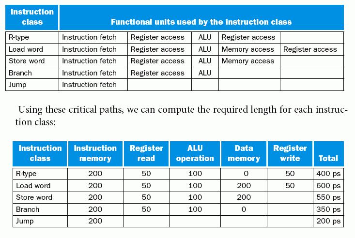
65 Single Cycle Implementation Exercise: Assuming we have the following instruction mix: Load 25% Store 10% ALU instructions 45% Branch 15% Jump 5% Calculate cycle time and total program (with L instructions) execution time Assuming negligible delays except for the following: memory (200 ps) (ps = Pico Second) ALU and adders (100 ps) Register file access (50 ps) Note: For single-cycle instruction, CPI = 1 Answer: (Complete answer) 65
66 Single Cycle Problems Single cycle instruction is not used in modern computers Disadvantages: Inefficient in both performance and HW cost Clock cycle must have the same length for every instruction Clock cycle determined by the longest possible path For complicated instruction like floating point, it will be harder Functional units must be duplicated, since each can be used only once per cycle 66
CPU DESIGN The Single-Cycle Implementation
 CSE 202 Computer Organization CPU DESIGN The Single-Cycle Implementation Shakil M. Khan (adapted from Prof. H. Roumani) Dept of CS & Eng, York University Sequential vs. Combinational Circuits Digital circuits
Project Two RISC Processor Implementation ECE 485
 Project Two RISC Processor Implementation ECE 485 Chenqi Bao Peter Chinetti November 6, 2013 Instructor: Professor Borkar 1 Statement of Problem This project requires the design and test of a RISC processor
Review. Combined Datapath
 Review Topics:. A single cycle implementation 2. State Diagrams. A mltiple cycle implementation COSC 22: Compter Organization Instrctor: Dr. Amir Asif Department of Compter Science York University Handot
EC 413 Computer Organization
 EC 413 Computer Organization rithmetic Logic Unit (LU) and Register File Prof. Michel. Kinsy Computing: Computer Organization The DN of Modern Computing Computer CPU Memory System LU Register File Disks
CSE Computer Architecture I
 Execution Sequence Summary CSE 30321 Computer Architecture I Lecture 17 - Multi Cycle Control Michael Niemier Department of Computer Science and Engineering Step name Instruction fetch Instruction decode/register
Processor Design & ALU Design
 3/8/2 Processor Design A. Sahu CSE, IIT Guwahati Please be updated with http://jatinga.iitg.ernet.in/~asahu/c22/ Outline Components of CPU Register, Multiplexor, Decoder, / Adder, substractor, Varity of
Implementing the Controller. Harvard-Style Datapath for DLX
 6.823, L6--1 Implementing the Controller Laboratory for Computer Science M.I.T. http://www.csg.lcs.mit.edu/6.823 6.823, L6--2 Harvard-Style Datapath for DLX Src1 ( j / ~j ) Src2 ( R / RInd) RegWrite MemWrite
L07-L09 recap: Fundamental lesson(s)!
!") L7-L9 recap: Fundamental lesson(s)! Over the next 3 lectures (using the IPS ISA as context) I ll explain:! How functions are treated and processed in assembly! How system calls are enabled in assembly!
L7-L9 recap: Fundamental lesson(s)! Over the next 3 lectures (using the IPS ISA as context) I ll explain:! How functions are treated and processed in assembly! How system calls are enabled in assembly!
Spiral 1 / Unit 3
 -3. Spiral / Unit 3 Minterm and Maxterms Canonical Sums and Products 2- and 3-Variable Boolean Algebra Theorems DeMorgan's Theorem Function Synthesis use Canonical Sums/Products -3.2 Outcomes I know the
61C In the News. Processor Design: 5 steps
 www.eetimes.com/electronics-news/23235/thailand-floods-take-toll-on--makers The Thai floods have already claimed the lives of hundreds of pele, with tens of thousands more having had to flee their homes
Review: Single-Cycle Processor. Limits on cycle time
 Review: Single-Cycle Processor Jump 3:26 5: MemtoReg Control Unit LUControl 2: Op Funct LUSrc RegDst PCJump PC 4 uction + PCPlus4 25:2 2:6 2:6 5: 5: 2 3 WriteReg 4: Src Src LU Zero LUResult Write + PC
CPSC 3300 Spring 2017 Exam 2
 CPSC 3300 Spring 2017 Exam 2 Name: 1. Matching. Write the correct term from the list into each blank. (2 pts. each) structural hazard EPIC forwarding precise exception hardwired load-use data hazard VLIW
Control. Control. the ALU. ALU control signals 11/4/14. Next: control. We built the instrument. Now we read music and play it...
 // CS 2, Fall 2! CS 2, Fall 2! We built the instrument. Now we read music and play it... A simple implementa/on uc/on uct r r 2 Write r Src Src Extend 6 Mem Next: path 7-2 CS 2, Fall 2! signals CS 2, Fall
3. (2) What is the difference between fixed and hybrid instructions?
 What is the difference between fixed and hybrid instructions?") 1. (2 pts) What is a "balanced" pipeline? 2. (2 pts) What are the two main ways to define performance? 3. (2) What is the difference between fixed and hybrid instructions? 4. (2 pts) Clock rates have grown
1. (2 pts) What is a "balanced" pipeline? 2. (2 pts) What are the two main ways to define performance? 3. (2) What is the difference between fixed and hybrid instructions? 4. (2 pts) Clock rates have grown
Simple Instruction-Pipelining. Pipelined Harvard Datapath
 6.823, L8--1 Simple ruction-pipelining Laboratory for Computer Science M.I.T. http://www.csg.lcs.mit.edu/6.823 Pipelined Harvard path 6.823, L8--2. I fetch decode & eg-fetch execute memory Clock period
Simple Instruction-Pipelining. Pipelined Harvard Datapath
 6.823, L8--1 Simple ruction-pipelining Updated March 6, 2000 Laboratory for Computer Science M.I.T. http://www.csg.lcs.mit.edu/6.823 Pipelined Harvard path 6.823, L8--2. fetch decode & eg-fetch execute
[2] Predicting the direction of a branch is not enough. What else is necessary?
![[2] Predicting the direction of a branch is not enough. What else is necessary?](/thumbs/74/69860001.jpg "[2] Predicting the direction of a branch is not enough. What else is necessary?") [2] What are the two main ways to define performance? [2] Predicting the direction of a branch is not enough. What else is necessary? [2] The power consumed by a chip has increased over time, but the clock
[2] What are the two main ways to define performance? [2] Predicting the direction of a branch is not enough. What else is necessary? [2] The power consumed by a chip has increased over time, but the clock
TEST 1 REVIEW. Lectures 1-5
 TEST 1 REVIEW Lectures 1-5 REVIEW Test 1 will cover lectures 1-5. There are 10 questions in total with the last being a bonus question. The questions take the form of short answers (where you are expected
[2] Predicting the direction of a branch is not enough. What else is necessary?
![[2] Predicting the direction of a branch is not enough. What else is necessary?](/thumbs/74/69859984.jpg "[2] Predicting the direction of a branch is not enough. What else is necessary?") [2] When we talk about the number of operands in an instruction (a 1-operand or a 2-operand instruction, for example), what do we mean? [2] What are the two main ways to define performance? [2] Predicting
[2] When we talk about the number of operands in an instruction (a 1-operand or a 2-operand instruction, for example), what do we mean? [2] What are the two main ways to define performance? [2] Predicting
1. (2 )Clock rates have grown by a factor of 1000 while power consumed has only grown by a factor of 30. How was this accomplished?
Clock rates have grown by a factor of 1000 while power consumed has only grown by a factor of 30. How was this accomplished?") 1. (2 )Clock rates have grown by a factor of 1000 while power consumed has only grown by a factor of 30. How was this accomplished? 2. (2 )What are the two main ways to define performance? 3. (2 )What
1. (2 )Clock rates have grown by a factor of 1000 while power consumed has only grown by a factor of 30. How was this accomplished? 2. (2 )What are the two main ways to define performance? 3. (2 )What
Topics: A multiple cycle implementation. Distributed Notes
 COSC 22: Compter Organization Instrctor: Dr. Amir Asif Department of Compter Science York University Handot # lticycle Implementation of a IPS Processor Topics: A mltiple cycle implementation Distribted
4. (3) What do we mean when we say something is an N-operand machine?
 What do we mean when we say something is an N-operand machine?") 1. (2) What are the two main ways to define performance? 2. (2) When dealing with control hazards, a prediction is not enough - what else is necessary in order to eliminate stalls? 3. (3) What is an "unbalanced"
1. (2) What are the two main ways to define performance? 2. (2) When dealing with control hazards, a prediction is not enough - what else is necessary in order to eliminate stalls? 3. (3) What is an "unbalanced"
Design of Digital Circuits Lecture 14: Microprogramming. Prof. Onur Mutlu ETH Zurich Spring April 2017
 Design of Digital Circuits Lecture 4: Microprogramming Prof. Onur Mutlu ETH Zurich Spring 27 7 April 27 Agenda for Today & Next Few Lectures! Single-cycle Microarchitectures! Multi-cycle and Microprogrammed
Building a Computer. Quiz #2 on 10/31, open book and notes. (This is the last lecture covered) I wonder where this goes? L16- Building a Computer 1
 I wonder where this goes? L16- Building a Computer 1") Building a Computer I wonder where this goes? B LU MIPS Kit Quiz # on /3, open book and notes (This is the last lecture covered) Comp 4 Fall 7 /4/7 L6- Building a Computer THIS IS IT! Motivating Force
Building a Computer I wonder where this goes? B LU MIPS Kit Quiz # on /3, open book and notes (This is the last lecture covered) Comp 4 Fall 7 /4/7 L6- Building a Computer THIS IS IT! Motivating Force
Lecture 13: Sequential Circuits, FSM
 Lecture 13: Sequential Circuits, FSM Today s topics: Sequential circuits Finite state machines 1 Clocks A microprocessor is composed of many different circuits that are operating simultaneously if each
Enrico Nardelli Logic Circuits and Computer Architecture
 Enrico Nardelli Logic Circuits and Computer Architecture Appendix B The design of VS0: a very simple CPU Rev. 1.4 (2009-10) by Enrico Nardelli B - 1 Instruction set Just 4 instructions LOAD M - Copy into
 CS 52 Computer rchitecture and Engineering Lecture 4 - Pipelining Krste sanovic Electrical Engineering and Computer Sciences University of California at Berkeley http://www.eecs.berkeley.edu/~krste! http://inst.eecs.berkeley.edu/~cs52!
Designing Single-Cycle MIPS Processor
 CSE 32: Introdction to Compter Architectre Designing Single-Cycle IPS Processor Presentation G Stdy:.-. Gojko Babić 2/9/28 Introdction We're now ready to look at an implementation of the system that incldes
Simple Instruction-Pipelining (cont.) Pipelining Jumps
 Pipelining Jumps") 6.823, L9--1 Simple ruction-pipelining (cont.) + Interrupts Updated March 6, 2000 Laboratory for Computer Science M.I.T. http://www.csg.lcs.mit.edu/6.823 Src1 ( j / ~j ) Src2 ( / Ind) Pipelining Jumps
6.823, L9--1 Simple ruction-pipelining (cont.) + Interrupts Updated March 6, 2000 Laboratory for Computer Science M.I.T. http://www.csg.lcs.mit.edu/6.823 Src1 ( j / ~j ) Src2 ( / Ind) Pipelining Jumps
Arithmetic and Logic Unit First Part
 Arithmetic and Logic Unit First Part Arquitectura de Computadoras Arturo Díaz D PérezP Centro de Investigación n y de Estudios Avanzados del IPN adiaz@cinvestav.mx Arquitectura de Computadoras ALU1-1 Typical
Outcomes. Spiral 1 / Unit 2. Boolean Algebra BOOLEAN ALGEBRA INTRO. Basic Boolean Algebra Logic Functions Decoders Multiplexers
 -2. -2.2 piral / Unit 2 Basic Boolean Algebra Logic Functions Decoders Multipleers Mark Redekopp Outcomes I know the difference between combinational and sequential logic and can name eamples of each.
UNIVERSITY OF WISCONSIN MADISON
 CS/ECE 252: INTRODUCTION TO COMPUTER ENGINEERING UNIVERSITY OF WISCONSIN MADISON Prof. Gurindar Sohi TAs: Minsub Shin, Lisa Ossian, Sujith Surendran Midterm Examination 2 In Class (50 minutes) Friday,
Computer Architecture. ECE 361 Lecture 5: The Design Process & ALU Design. 361 design.1
 Computer Architecture ECE 361 Lecture 5: The Design Process & Design 361 design.1 Quick Review of Last Lecture 361 design.2 MIPS ISA Design Objectives and Implications Support general OS and C- style language
Lecture 13: Sequential Circuits, FSM
 Lecture 13: Sequential Circuits, FSM Today s topics: Sequential circuits Finite state machines Reminder: midterm on Tue 2/28 will cover Chapters 1-3, App A, B if you understand all slides, assignments,
A Second Datapath Example YH16
 A Second Datapath Example YH16 Lecture 09 Prof. Yih Huang S365 1 A 16-Bit Architecture: YH16 A word is 16 bit wide 32 general purpose registers, 16 bits each Like MIPS, 0 is hardwired zero. 16 bit P 16
CMP 334: Seventh Class
 CMP 334: Seventh Class Performance HW 5 solution Averages and weighted averages (review) Amdahl's law Ripple-carry adder circuits Binary addition Half-adder circuits Full-adder circuits Subtraction, negative
Pipelining. Traditional Execution. CS 365 Lecture 12 Prof. Yih Huang. add ld beq CS CS 365 2
 Pipelining CS 365 Lecture 12 Prof. Yih Huang CS 365 1 Traditional Execution 1 2 3 4 1 2 3 4 5 1 2 3 add ld beq CS 365 2 1 Pipelined Execution 1 2 3 4 5 1 2 3 4 5 1 2 3 4 5 1 2 3 4 5 1 2 3 4 5 1 2 3 4 5
Designing MIPS Processor
 CSE 675.: Introdction to Compter Architectre Designing IPS Processor (lti-cycle) Presentation H Reading Assignment: 5.5,5.6 lti-cycle Design Principles Break p eection of each instrction into steps. The
CSc 256 Midterm 2 Fall 2010
 CSc 256 Midterm 2 Fall 2010 NAME: 1a)YouaregivenaMIPSbranchinstruction: x:beq$12,$0,y Theaddressofthelabel"y"is0x40013c.Thememorylocationat"x"contains: addresscontents 0x4002080001000110000000????????????????...whichrepresentsthebeqinstruction;the????...????arethe
Lecture 3, Performance
 Lecture 3, Performance Repeating some definitions: CPI Clocks Per Instruction MHz megahertz, millions of cycles per second MIPS Millions of Instructions Per Second = MHz / CPI MOPS Millions of Operations
CSCI-564 Advanced Computer Architecture
 CSCI-564 Advanced Computer Architecture Lecture 8: Handling Exceptions and Interrupts / Superscalar Bo Wu Colorado School of Mines Branch Delay Slots (expose control hazard to software) Change the ISA
Chapter 5. Digital Design and Computer Architecture, 2 nd Edition. David Money Harris and Sarah L. Harris. Chapter 5 <1>
 Chapter 5 Digital Design and Computer Architecture, 2 nd Edition David Money Harris and Sarah L. Harris Chapter 5 Chapter 5 :: Topics Introduction Arithmetic Circuits umber Systems Sequential Building
Computer Architecture ELEC2401 & ELEC3441
 Last Time Pipeline Hazard Computer Architecture ELEC2401 & ELEC3441 Lecture 8 Pipelining (3) Dr. Hayden Kwok-Hay So Department of Electrical and Electronic Engineering Structural Hazard Hazard Control
Microprocessor Power Analysis by Labeled Simulation
 Microprocessor Power Analysis by Labeled Simulation Cheng-Ta Hsieh, Kevin Chen and Massoud Pedram University of Southern California Dept. of EE-Systems Los Angeles CA 989 Outline! Introduction! Problem
COVER SHEET: Problem#: Points
 EEL 4712 Midterm 3 Spring 2017 VERSION 1 Name: UFID: Sign here to give permission for your test to be returned in class, where others might see your score: IMPORTANT: Please be neat and write (or draw)
Logic and Computer Design Fundamentals. Chapter 8 Sequencing and Control
 Logic and Computer Design Fundamentals Chapter 8 Sequencing and Control Datapath and Control Datapath - performs data transfer and processing operations Control Unit - Determines enabling and sequencing
ECE 3401 Lecture 23. Pipeline Design. State Table for 2-Cycle Instructions. Control Unit. ISA: Instruction Specifications (for reference)
") ECE 3401 Lecture 23 Pipeline Design Control State Register Combinational Control Logic New/ Modified Control Word ISA: Instruction Specifications (for reference) P C P C + 1 I N F I R M [ P C ] E X 0 PC
ECE 3401 Lecture 23 Pipeline Design Control State Register Combinational Control Logic New/ Modified Control Word ISA: Instruction Specifications (for reference) P C P C + 1 I N F I R M [ P C ] E X 0 PC
Numbers and Arithmetic
 Numbers and Arithmetic See: P&H Chapter 2.4 2.6, 3.2, C.5 C.6 Hakim Weatherspoon CS 3410, Spring 2013 Computer Science Cornell University Big Picture: Building a Processor memory inst register file alu
Design at the Register Transfer Level
 Week-7 Design at the Register Transfer Level Algorithmic State Machines Algorithmic State Machine (ASM) q Our design methodologies do not scale well to real-world problems. q 232 - Logic Design / Algorithmic
Numbers and Arithmetic
 Numbers and Arithmetic See: P&H Chapter 2.4 2.6, 3.2, C.5 C.6 Hakim Weatherspoon CS 3410, Spring 2013 Computer Science Cornell University Big Picture: Building a Processor memory inst register file alu
CprE 281: Digital Logic
 CprE 28: Digital Logic Instructor: Alexander Stoytchev http://www.ece.iastate.edu/~alexs/classes/ Simple Processor CprE 28: Digital Logic Iowa State University, Ames, IA Copyright Alexander Stoytchev Digital
Lecture 3, Performance
 Repeating some definitions: Lecture 3, Performance CPI MHz MIPS MOPS Clocks Per Instruction megahertz, millions of cycles per second Millions of Instructions Per Second = MHz / CPI Millions of Operations
Figure 4.9 MARIE s Datapath
 Term Control Word Microoperation Hardwired Control Microprogrammed Control Discussion A set of signals that executes a microoperation. A register transfer or other operation that the CPU can execute in
Computer Architecture
 Lecture 2: Iakovos Mavroidis Computer Science Department University of Crete 1 Previous Lecture CPU Evolution What is? 2 Outline Measurements and metrics : Performance, Cost, Dependability, Power Guidelines
Design. Dr. A. Sahu. Indian Institute of Technology Guwahati
 CS222: Processor Design: Multi Cycle Design Dr. A. Sahu Dept of Comp. Sc. & Engg. Indian Institute of Technology Guwahati Mid Semester Exam Multi Cycle design Outline Clock periods in single cycle and
CMP N 301 Computer Architecture. Appendix C
 CMP N 301 Computer Architecture Appendix C Outline Introduction Pipelining Hazards Pipelining Implementation Exception Handling Advanced Issues (Dynamic Scheduling, Out of order Issue, Superscalar, etc)
Appendix B. Review of Digital Logic. Baback Izadi Division of Engineering Programs
 Appendix B Review of Digital Logic Baback Izadi Division of Engineering Programs bai@engr.newpaltz.edu Elect. & Comp. Eng. 2 DeMorgan Symbols NAND (A.B) = A +B NOR (A+B) = A.B AND A.B = A.B = (A +B ) OR
Design of Sequential Circuits
 Design of Sequential Circuits Seven Steps: Construct a state diagram (showing contents of flip flop and inputs with next state) Assign letter variables to each flip flop and each input and output variable
CA Compiler Construction
 CA4003 - Compiler Construction Code Generation to MIPS David Sinclair Code Generation The generation o machine code depends heavily on: the intermediate representation;and the target processor. We are
ICS 233 Computer Architecture & Assembly Language
 ICS 233 Computer Architecture & Assembly Language Assignment 6 Solution 1. Identify all of the RAW data dependencies in the following code. Which dependencies are data hazards that will be resolved by
Verilog HDL:Digital Design and Modeling. Chapter 11. Additional Design Examples. Additional Figures
 Chapter Additional Design Examples Verilog HDL:Digital Design and Modeling Chapter Additional Design Examples Additional Figures Chapter Additional Design Examples 2 Page 62 a b y y 2 y 3 c d e f Figure
CHAPTER log 2 64 = 6 lines/mux or decoder 9-2.* C = C 8 V = C 8 C * 9-4.* (Errata: Delete 1 after problem number) 9-5.
 9-5.") CHPTER 9 2008 Pearson Education, Inc. 9-. log 2 64 = 6 lines/mux or decoder 9-2.* C = C 8 V = C 8 C 7 Z = F 7 + F 6 + F 5 + F 4 + F 3 + F 2 + F + F 0 N = F 7 9-3.* = S + S = S + S S S S0 C in C 0 dder
CHPTER 9 2008 Pearson Education, Inc. 9-. log 2 64 = 6 lines/mux or decoder 9-2.* C = C 8 V = C 8 C 7 Z = F 7 + F 6 + F 5 + F 4 + F 3 + F 2 + F + F 0 N = F 7 9-3.* = S + S = S + S S S S0 C in C 0 dder
State and Finite State Machines
 State and Finite State Machines See P&H Appendix C.7. C.8, C.10, C.11 Hakim Weatherspoon CS 3410, Spring 2013 Computer Science Cornell University Big Picture: Building a Processor memory inst register
Formal Verification of Systems-on-Chip
 Formal Verification of Systems-on-Chip Wolfgang Kunz Department of Electrical & Computer Engineering University of Kaiserslautern, Germany Slide 1 Industrial Experiences Formal verification of Systems-on-Chip
Instruction register. Data. Registers. Register # Memory data register
 Where we are headed Single Cycle Problems: what if we had a more complicated instrction like floating point? wastefl of area One Soltion: se a smaller cycle time have different instrctions take different
Basic Computer Organization and Design Part 3/3
 Basic Computer Organization and Design Part 3/3 Adapted by Dr. Adel Ammar Computer Organization Interrupt Initiated Input/Output Open communication only when some data has to be passed --> interrupt. The
Table of Content. Chapter 11 Dedicated Microprocessors Page 1 of 25
 Chapter 11 Dedicated Microprocessors Page 1 of 25 Table of Content Table of Content... 1 11 Dedicated Microprocessors... 2 11.1 Manual Construction of a Dedicated Microprocessor... 3 11.2 FSM + D Model
Department of Electrical and Computer Engineering The University of Texas at Austin
 Department of Electrical and Computer Engineering The University of Texas at Austin EE 360N, Fall 2004 Yale Patt, Instructor Aater Suleman, Huzefa Sanjeliwala, Dam Sunwoo, TAs Exam 1, October 6, 2004 Name:
ECE 2300 Digital Logic & Computer Organization
 ECE 2300 Digital Logic & Computer Organization pring 201 More inary rithmetic LU 1 nnouncements Lab 4 prelab () due tomorrow Lab 5 to be released tonight 2 Example: Fixed ize 2 C ddition White stone =
Hakim Weatherspoon CS 3410 Computer Science Cornell University
 Hakim Weatherspoon CS 3410 Computer Science Cornell University The slides are the product of many rounds of teaching CS 3410 by Professors Weatherspoon, Bala, Bracy, and Sirer. memory inst 32 register
EXAMPLES 4/12/2018. The MIPS Pipeline. Hazard Summary. Show the pipeline diagram. Show the pipeline diagram. Pipeline Datapath and Control
 The MIPS Pipeline CSCI206 - Computer Organization & Programming Pipeline Datapath and Control zybook: 11.6 Developed and maintained by the Bucknell University Computer Science Department - 2017 Hazard
Spiral 2-1. Datapath Components: Counters Adders Design Example: Crosswalk Controller
 2-. piral 2- Datapath Components: Counters s Design Example: Crosswalk Controller 2-.2 piral Content Mapping piral Theory Combinational Design equential Design ystem Level Design Implementation and Tools
CPU DESIGN The Single-Cycle Implementation
 22 ompter Organization Seqential vs. ombinational ircits Digital circits can be classified into two categories: DESIGN The Single-ycle Implementation. ombinational ircits: m, 2. Seqential ircits: flip-flops,
LABORATORY MANUAL MICROPROCESSOR AND MICROCONTROLLER
 LABORATORY MANUAL S u b j e c t : MICROPROCESSOR AND MICROCONTROLLER TE (E lectr onics) ( S e m V ) 1 I n d e x Serial No T i tl e P a g e N o M i c r o p r o c e s s o r 8 0 8 5 1 8 Bit Addition by Direct
Lecture 9: Control Hazard and Resolution. James C. Hoe Department of ECE Carnegie Mellon University
 18 447 Lectre 9: Control Hazard and Resoltion James C. Hoe Department of ECE Carnegie ellon University 18 447 S18 L09 S1, James C. Hoe, CU/ECE/CALC, 2018 Yor goal today Hosekeeping simple control flow
EECS150 - Digital Design Lecture 11 - Shifters & Counters. Register Summary
 EECS50 - Digital Design Lecture - Shifters & Counters February 24, 2003 John Wawrzynek Spring 2005 EECS50 - Lec-counters Page Register Summary All registers (this semester) based on Flip-flops: q 3 q 2
CMPEN 411 VLSI Digital Circuits Spring Lecture 19: Adder Design
 CMPEN 411 VLSI Digital Circuits Spring 2011 Lecture 19: Adder Design [Adapted from Rabaey s Digital Integrated Circuits, Second Edition, 2003 J. Rabaey, A. Chandrakasan, B. Nikolic] Sp11 CMPEN 411 L19
CS61C : Machine Structures
 CS 61C L15 Blocks (1) inst.eecs.berkeley.edu/~cs61c/su05 CS61C : Machine Structures Lecture #15: Combinational Logic Blocks Outline CL Blocks Latches & Flip Flops A Closer Look 2005-07-14 Andy Carle CS
EXPERIMENT Bit Binary Sequential Multiplier
 12.1 Objectives EXPERIMENT 12 12. -Bit Binary Sequential Multiplier Introduction of large digital system design, i.e. data path and control path. To apply the above concepts to the design of a sequential
System Data Bus (8-bit) Data Buffer. Internal Data Bus (8-bit) 8-bit register (R) 3-bit address 16-bit register pair (P) 2-bit address
 Data Buffer. Internal Data Bus (8-bit) 8-bit register (R) 3-bit address 16-bit register pair (P) 2-bit address") Intel 8080 CPU block diagram 8 System Data Bus (8-bit) Data Buffer Registry Array B 8 C Internal Data Bus (8-bit) F D E H L ALU SP A PC Address Buffer 16 System Address Bus (16-bit) Internal register addressing:
Intel 8080 CPU block diagram 8 System Data Bus (8-bit) Data Buffer Registry Array B 8 C Internal Data Bus (8-bit) F D E H L ALU SP A PC Address Buffer 16 System Address Bus (16-bit) Internal register addressing:
NCU EE -- DSP VLSI Design. Tsung-Han Tsai 1
 NCU EE -- DSP VLSI Design. Tsung-Han Tsai 1 Multi-processor vs. Multi-computer architecture µp vs. DSP RISC vs. DSP RISC Reduced-instruction-set Register-to-register operation Higher throughput by using
Review: Designing with FSM. EECS Components and Design Techniques for Digital Systems. Lec09 Counters Outline.
 Review: Designing with FSM EECS 150 - Components and Design Techniques for Digital Systems Lec09 Counters 9-28-04 David Culler Electrical Engineering and Computer Sciences University of California, Berkeley
State & Finite State Machines
 State & Finite State Machines Hakim Weatherspoon CS 3410, Spring 2012 Computer Science Cornell University See P&H Appendix C.7. C.8, C.10, C.11 Big Picture: Building a Processor memory inst register file
CS61C : Machine Structures
 inst.eecs.berkeley.edu/~cs61c/su05 CS61C : Machine Structures Lecture #15: Combinational Logic Blocks 2005-07-14 CS 61C L15 Blocks (1) Andy Carle Outline CL Blocks Latches & Flip Flops A Closer Look CS
Computer Architecture
 Computer Architecture QtSpim, a Mips simulator S. Coudert and R. Pacalet January 4, 2018..................... Memory Mapping 0xFFFF000C 0xFFFF0008 0xFFFF0004 0xffff0000 0x90000000 0x80000000 0x7ffff4d4
Clock T FF1 T CL1 T FF2 T T T FF T T FF T CL T FF T CL T FF T T FF T T FF T CL. T cyc T H. Clock T FF T T FF T CL T FF T T FF T CL.
 etup TA 60 c, vcc 3v Hold TA 30 c, vcc 5v Tkew TL TL TH FF FF 2 T cyc T H T L Clock TpdFF 2 TpdCL2Tetup FF Tcyc TL 2 2 TpdFF TpdCL Tetup FF2 TH 2 T FF T T FF T CL Hold L cd cd T FF T T FF T CL Hold L cd
ECE290 Fall 2012 Lecture 22. Dr. Zbigniew Kalbarczyk
 ECE290 Fall 2012 Lecture 22 Dr. Zbigniew Kalbarczyk Today LC-3 Micro-sequencer (the control store) LC-3 Micro-programmed control memory LC-3 Micro-instruction format LC -3 Micro-sequencer (the circuitry)
Preparation of Examination Questions and Exercises: Solutions
 Questions Preparation of Examination Questions and Exercises: Solutions. -bit Subtraction: DIF = B - BI B BI BO DIF 2 DIF: B BI 4 6 BI 5 BO: BI BI 4 5 7 3 2 6 7 3 B B B B B DIF = B BI ; B = ( B) BI ( B),
CPS 104 Computer Organization and Programming Lecture 11: Gates, Buses, Latches. Robert Wagner
 CPS 4 Computer Organization and Programming Lecture : Gates, Buses, Latches. Robert Wagner CPS4 GBL. RW Fall 2 Overview of Today s Lecture: The MIPS ALU Shifter The Tristate driver Bus Interconnections
ALU A functional unit
 ALU A functional unit that performs arithmetic operations such as ADD, SUB, MPY logical operations such as AND, OR, XOR, NOT on given data types: 8-,16-,32-, or 64-bit values A n-1 A n-2... A 1 A 0 B n-1
Implementing Absolute Addressing in a Motorola Processor (DRAFT)
") Implementing Absolute Addressing in a Motorola 68000 Processor (DRAFT) Dylan Leigh (s3017239) 2009 This project involved the further development of a limited 68000 processor core, developed by Dylan Leigh
Implementing Absolute Addressing in a Motorola 68000 Processor (DRAFT) Dylan Leigh (s3017239) 2009 This project involved the further development of a limited 68000 processor core, developed by Dylan Leigh
Solutions for Appendix C Exercises
 C Solutions for Appix C Exercises 1 Solutions for Appix C Exercises C.1 A B A B A + B A B A B A + B 0 0 1 1 1 1 1 1 0 1 1 0 0 0 1 1 1 0 0 1 0 0 1 1 1 1 0 0 0 0 0 0 C.2 Here is the first equation: E = ((
Review: Designing with FSM. EECS Components and Design Techniques for Digital Systems. Lec 09 Counters Outline.
 Review: esigning with FSM EECS 150 - Components and esign Techniques for igital Systems Lec 09 Counters 9-28-0 avid Culler Electrical Engineering and Computer Sciences University of California, Berkeley
Digital Integrated Circuits A Design Perspective. Arithmetic Circuits. Jan M. Rabaey Anantha Chandrakasan Borivoje Nikolic.
 Digital Integrated Circuits A Design Perspective Jan M. Rabaey Anantha Chandrakasan Borivoje Nikolic Arithmetic Circuits January, 2003 1 A Generic Digital Processor MEMORY INPUT-OUTPUT CONTROL DATAPATH
Chapter 9 Computer Design Basics
 Logic ad Computer Desig Fudametals Chapter 9 Computer Desig Basics Part 1 Datapaths Overview Part 1 Datapaths Itroductio Datapath Example Arithmetic Logic Uit (ALU) Shifter Datapath Represetatio Cotrol
Practice Homework Solution for Module 4
 Practice Homework Solution for Module 4 1. Tired of writing the names of those you want kicked off the island on cards, you wish to modernize the voting scheme used on Digital Survivor. Specifically, you
ECEN 651: Microprogrammed Control of Digital Systems Department of Electrical and Computer Engineering Texas A&M University
 ECEN 651: Microprogrammed Control of Digital Systems Department of Electrical and Computer Engineering Texas A&M University Prof. Mi Lu TA: Ehsan Rohani Laboratory Exercise #4 MIPS Assembly and Simulation
Lecture 12: Pipelined Implementations: Control Hazards and Resolutions
 18-447 Lectre 12: Pipelined Implementations: Control Hazards and Resoltions S 09 L12-1 James C. Hoe Dept of ECE, CU arch 2, 2009 Annoncements: Spring break net week!! Project 2 de the week after spring
Computer Architecture. ESE 345 Computer Architecture. Design Process. CA: Design process
 Computer Architecture ESE 345 Computer Architecture Design Process 1 The Design Process "To Design Is To Represent" Design activity yields description/representation of an object -- Traditional craftsman
CSE Computer Architecture I
 Single cycle Conrol Implemenaion CSE 332 Compuer Archiecure I l x I Lecure 7 - uli Cycle achines i i [ ] I I r l ichael Niemier Deparmen of Compuer Science and Engineering I ] i X.S. Hu 5- X.S. Hu 5-2