Lecture 4. Detectors for Ionizing Particles
|
|
|
- Patricia Farmer
- 6 years ago
- Views:
Transcription
1 Lecture 4 Detectors for Ionizing Particles
2 Introduction Overview of detector systems Sources of radiation Radioactive decay Cosmic Radiation Accelerators Content Interaction of Radiation with Matter General principles Charged particles heavy charged particles electrons Neutral particles Photons Neutrons Neutrinos Definitions Detectors for Ionizing Particles Principles of ionizing detectors Semiconductor detectors Semiconductor basics Sensor concepts
3 Semiconductor detectors Different detector materials Readout electronics Gas detectors Principles Detector concepts Scintillation detectors General characteristics Organic materials Inorganic materials Light output response Content Velocity Determination in Dielectric Media Cerenkov detectors Cerenkov radiation Cerenkov detectors Transition Radiation detectors Phenomenology of Transition Radiation Detection of Transition Radiation Complex Detector Systems Particle Identification with Combined Detector Information Tracking
4 Review of Previous Lecture
5 Absorption of Photons Photoelectric effect: Compton scattering Pair production near nuclei
6 Interaction of Neutrons No electric charge è no Coulomb interaction Only strong force with nuclei in matter High energy neutrons have to come within cm of the nucleus è very penetrating Several different interaction processes: Elastic scattering: Principal mechanism of energy loss in the range of MeV Inelastic scattering: Nucleus is left in an excited state which later decays by radiative emission. Energy of neutron has to be high enough for excitation (typically > 1 MeV) Radiative neutron capture: cross section 1/v è only takes place for slow neutrons, resonance peaks superimposed Other nuclear reaction: caption of neutron + emission of charged particle, typically in the range of ev to kev, cross section 1/v + resonances Fission: most likely at thermal energies High energy hadron shower production: only for very high energy neutrons (> 100 MeV)
 Momentum of ν has to be sufficient Elastic Scattering Detection of the scattered electron")
7 Neutrino Measuring Techniques Radio chemical method Detection via radioactive reaction products Only sensitve on ν e!! Measurement of the partner lepton Sensitive on ν e and ν µ (+ ν τ ) Momentum of ν has to be sufficient Elastic Scattering Detection of the scattered electron Deuteron breaking Detection of the nucleons
8 Start of Lecture 4 Definitions Semiconductor Detectors
9 Sensitivity is the minimum magnitude of input signal required to produce a specified output signal having a specified signal-to-noise ratio Usually given by: the cross section for ionization reactions in the detector the detector mass the inherent detector noise the protective material surrounding the detector determines the probability that (part of) the energy of the incoming radiation is transformed in the form of ionization signal > noise entrance threshold
10 Energy Resolution Width of the probability distribution function of the measured observable for a given physical value For detectors designed to measure the energy of the incident radiation the energy resolution is the most important quantity The resolution is quantified in terms of the full width at half maximum of the peak: R = Δ FWHM E / E = 2.35 σ(e) / E Two peaks closer together than the FWHM are usually considered not resolvable ΔE includes all type of noise sources: ( ) 2 ( ) 2 ( ) 2 ( ) 2 ΔE = ΔE + ΔE + ΔE +... stat det elect
11 Energy Resolution and Fano Factor The mean number of ionizing events J is given by the mean energy required to produce an ionization w (w > B.E.): J = E / w w depends on the material To calculate the fluctuations one would typically take the Poisson distribution which yields: var = J This implies that the ionization processes are all statistically independent, which is not true U. Fano calculated the variance for large J and found: var = σ 2 = FJ F is the Fano factor describing the deviation of the variance from a Poisson distribution This gives for the resolution: FJ R = 2.35 = J Fw E For F = 1 the variance is the same as the Poisson distribution
12 The Fano Factor Because the Fano factor describes corrections in the statistical fluctuations in the process of ionization it gives the best energy resolution a detector can reach It is material dependent and varies strongly: scintillators 1 gases < 1 semiconductors 0.1 (theoretically) Measuring the Fano factor not easy because all other noise sources have to be reduced è typically an upper limit for the Fano factor is given F is in addition a function of the temperature and, below 1 kev, also of the energy of the incoming particle
13 Detector Response In general the detector response describes the dependence of the expectation value of a measured quantity on the physical quantity Ideally the relation between the physical quantity and the measured quantity is linear (this is not necessary but makes life easier) Due to the limited resolution of the detector the result will always convoluted with the resolution Be careful: the response of a detector may vary with the type of radiation it detects
14 The Response Function Spectrum of pulse heights observed from the detector for a monoenergetic beam Ideal case: delta function and linear behavior for different energies è 1-to-1 correspondence between the measured quantity and the particles physical quantity Typically (much) more complicated: e.g.: electrons on a thick detector: main component: Gaussian distribution some electrons scatter out of detector è low energetic tail bremsstrahlung à photons leave detector è low energetic tail e.g.: photons on the same detector: è next page
15 The Response Function Superposition of photoelectric effect, Compton scattering and pair production Response function for a germanium detector and an organic scintillator detector for 661 kev gamma rays PH( E) = S( E') R( E, E') de' PH: pulse height distribution, R(E,E ) response function, S(E ) incident spectrum, E incident energy
16 Response Time Time between the arrival of the particle and the signal formation Important for dedicated time measurements (e.g. time-of-flight detectors) Must be considered when triggering on events in different detector components
17 Dead Time Finite time required by a detector to process an event, during which no additional signal can be registered Two cases: detector is insensitive à non-extendable/paralyzable dead time detector stays sensitive à extendable or paralyzable dead time (e.g. rate of a Geiger-Müller counter drops at at very high dosis)
18 Dead time Non-extendable dead time: mt = k + mkτ k T m = 1 ( k T ) τ m: true count rate, T: measuring time, k: measured counts, τ: dead time Extendable dead time: P(t): distribution of time intervals between random events with rate m P( t) = mexp( mt) only events arriving later than τ are recorded P( t > τ ) = m exp( mt) dt = exp( mτ ) τ k = mt exp( mτ )
19 Measuring dead time Two-source technique (for the non-extended case): f n n 1 1/ 2 + n R = 1 R 2 1/ 2 1/ 2τ R = 1 R 12 12τ τ = Large errors (5-10%) Experimentally difficult 12 R 1 R R R Better: use of two oscillators: f1 + = 1/ T Non-extendable dead time f 2 2 f1 f2τ for for < τ < T R1 R2 = + τ 1 Rτ 1 R τ [ R R / 2 T / 2 < τ < T ( R12 R R R R f f = 0 1 )( R + f R 2 )] 1/ 2 Extendable dead time 2 f1 f2τ for for 0 < τ < T T < τ with T: period of faster osc. τ = t m R1 + R2 2 R R 1 2 R 12 Equal for f < (2τ) -1
20 Two definitions: absolute efficiency E tot intrinsic efficiency E int Detector Efficiency E tot Example: cylindrical detector with a point source at a distance d on the axis of the detector P( θ) dω = dω / 4π x dω de tot = 1 exp λ 4π If x does not vary too much : E tot E int E geom = efficiency acceptance events registered events emitted by source events registered E int = events impinging on detector
21 Semiconductor Detectors

22 Insulator Semiconductor - Conductor 10-3 to 10 8 Ωcm
23 IV IV-IV III-V II-VI IV-VI Si SiC AlAs CdS PbS Ge AlSb CdSe PbTe yellow=most common Semiconductors Period II III IV V VI 2 Boron Carbon Nitrogen 3 Magnesium Aluminium Silicon Phosphorus Sulfur 4 Zinc Gallium Germanium Arsenic Selenium 5 Cadmium Indium Tin Antimony Tellurium 6 Mercury Lead BN GaAs GaP GaSb InAs InP InSb CdTe ZnS ZnSe ZnTe CdZnTe HgCdTe
24 Semiconductor Detectors A semiconductor detector is a solid state ionization chamber Gas Semiconductor Z E(e/ion) creation ev ev specific density 0.17 (He) 0.9 (Ne) g l (Si) 5.3 (Ge) g cm -3 pairs per length 100 e/ions per cm 100 e/h per µm e mobility O(1000 cm 2 /Vs) cm 2 /Vs ion(hole) mobility 1 2 cm 2 /Vs cm 2 /Vs
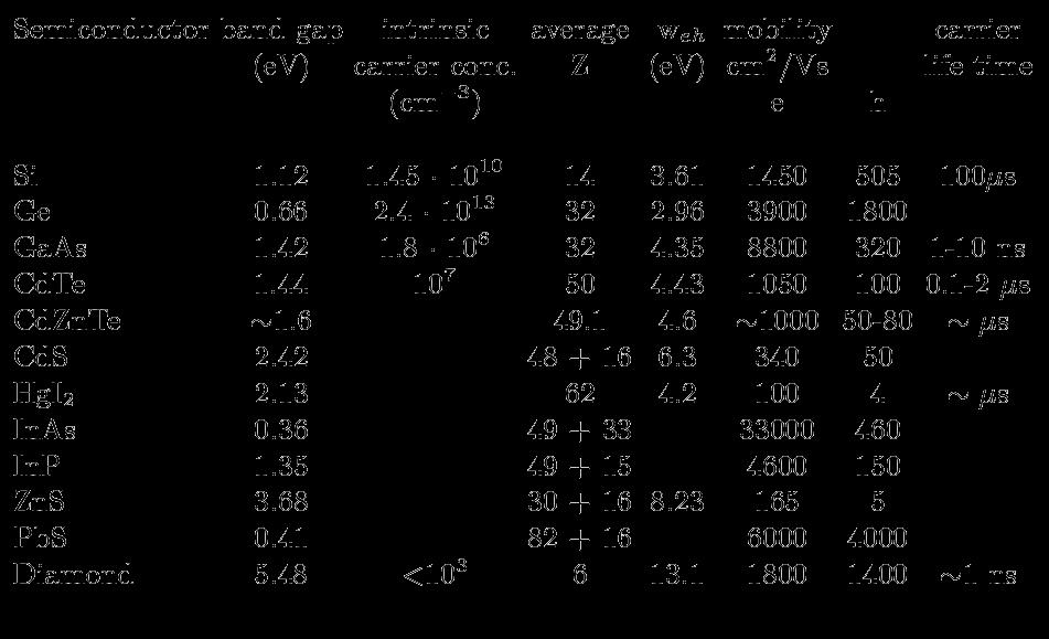
25 Semiconductors suited for Detectors


")
26 Lattices face centred cubic (fcc): diamond lattice (Si,Ge): cubic face centered lattice all atoms identical zinc blende lattice (GaAs): cubic face centered lattice different Atoms (Ga, As)
27 Energy bands I energy at r 0 E tot à min Degeneration of energy levels for close distances valence level e.g. p-level e.g. s-level r = distance between atoms

28 Energy bands II semi conductors metals band gap
29 Energy bands III Insulator Semi-conductor Conductor conduction band (empty) valence band (filled) E g ~10eV conduction band (empty) valence band (filled) E g ~1eV conduction band valence band type 1 type 2 conduction band part. filled Fermi-Dirac Statistics: room temperature 1/40 ev

30 Auger effect Auger effect: an electron from a higher shell to a vacant electronic state and ejecting an electron from the same higher shell. è Only levels near the edge are important

31 Brillouin zone Within a lattice the free electrons see the potential of the atoms For electrons all k-values are allowed but when the k meets the Bragg condition an interaction with the lattice happens Trick: create Brillouin zone: reciprocal lattice in k-space All k-vectors sitting at the boundary of the Brillouin zone fulfill Bragg condition
32 Effective mass Brillouin zones Simplified picture The electron wave function is reflected at the Brillouin boundaries è stationary wave with two solutions of the Schrödinger equation è forbidden areas Dispersion relation of a free electron gas 2 is not valid anymore E =! 2m k 2 Transition from true mass of electron to effective mass: 1 m * = 1 2 µν! dk µ dkν m* curvature of E(k) à m* < 0 possible d 2 E Tensor Equation of motion: * F = m v! g
33 Effective mass m e* /m e m h* /m e Si Ge GaAs
 several k-values for the same energy value possible à bands overlap in k-space k wide minimum è m * large (0.")
34 Direct and indirect semiconductors indirect e.g. Si, Ge direct e.g. GaAs to produce e/h must change E AND k narow minimum è m * small (0.07) several k-values for the same energy value possible à bands overlap in k-space k wide minimum è m * large (0.20) note: for the conduction mechanism only levels near the edges of the bands are important

35 Intrinsic conductivity at T > 0 a lattice bond can break valence electron becomes free leaves a hole behind this is a VB à CB transition the e - can move freely in CB the hole at position A is filled by an e - leaving another hole hole has effectively moved from A à B hole moves freely as well e - and hole move freely through the lattice as particles with different effective mass.
36 Density of states I
37 Density of states II
38 Density of states III
39 Carrier Concentration The number of free electrons can be calculated by the density of states in the conduction band Z(E) with the probability of their occupation given by the Fermi-Dirac function F(E): n = Z ( E ) F ( E )de Ec 0 with: F (E) = 1 1+ e ( E E F ) / kt e ( E E F ) / kt concentration of free electrons: 3/ 2 2π mn kt ( E E ) / kt n = 2 e C F 2!!h#!! " $ NC concentration of free holes: 3/ 2 2π m p kt ( EF EV ) / kt e p = 2 2 h!!#!! " $ NV with: EF the Fermi level mn (mp) the effective mass of the electrons and holes NC (NV) the effective density of states 2m * Z ( E )de = 4π 2 h 3 2 E de
40 Fermi level The product of electron and hole concentration is independent of the Fermi level: np = n 2 E i = NCNVe g / kt with E g = E C - E V This leads to intrinsic carrier concentration for silicon at 300 K to be: n i 10 3 = cm The intrinsic Fermi level is: E i = E 2 g 3kT + 4 m ln m p n Doping with donor or acceptor atoms changes the Fermi level: N N D E = + F Ei kt ln A E = F Ei kt ln ni ni


41 Doping of Semiconductors Electron Configuration for Si: K 2 L 8 M by bonding 8 group E g 1 ev n-type (donor) P, As, Sb 5 electrons in the M-shell 1 electron with binding energy mev p-type (acceptor) B, Al, Ga 3 electrons in the M-shell 1 electron missing

42 Doping n i = 1.45 x cm -3 typically n - = cm -3 n = cm -3 n + = cm -3
43 Donor and acceptor Levels
44 Donor and acceptor Levels
45 Donor and acceptor Levels

46 Ionisation energies for impurities states in the band gap E C Si ΔE E V E C GaAs ΔE E V

 E always!")
47 Drift of e and h in semiconductors drift velocity as a function of electric field strength saturation at ~10 7 cm/s v drift remember v = µ(e) E always! E(V/cm) typical Si - detector 100 V / 300 µm

48 Mobility as a function of temperature µ n (cm 2 /Vs) T 3/2 T -3/2 T(K) scattering at impurities scattering on lattice higher temp more lattice vibrations lower mobility

49 Try to make a detector Take a Si crystal of mm 3 volume resistivity Ge 0.49 Ωm at 300K Si some 100 Ωm due to impurities ~ free carriers A minimum ionizing particle would produce ~ e-h pairs
50 Get rid of free carriers
51 Get rid of free carriers Have to reduce the number of free carriers. Freeze out: Mobility, µ, conductivity, σ, majority [donors (e) acceptors (holes)] and minority [donors (holes) acceptors (e)] carrier concentration as function of temperature. n i is the intrinsic carrier density. or depletion

52 pn - junction p n
 ε n neutrality cond. Maxwell Electric field!! E( x) en ε = + en ε A D ( x + x ( x x p n ) ) for for x p < x < 0 0 < x < x n Potential 2 2 ( N x N x ) e V bi = A p + 2 ε D n")
53 pn junction as particle detector p + n - thin, highly doped p + (~10 19 cm -3 ) layer on lightly doped n - (~10 12 cm -3 ) substrate Space charge region N x = A de dx p N D x 1 = ρ( x) ε n neutrality cond. Maxwell Electric field!! E( x) en ε = + en ε A D ( x + x ( x x p n ) ) for for x p < x < 0 0 < x < x n Potential 2 2 ( N x N x ) e V bi = A p + 2 ε D n


54 pn junction under reverse bias (V ext ) 1. V bi! V bi + V ext 2. no thermal equilibrium => E F (n) E F (p) no bias Hole current Electron current p n forward bias Depletion region Depl. I p n reverse bias Depl. I

55 pn junction as particle detector Depletion zone grows from the junction into the lower doped bulk
56 Rules for junctions The chemical potential µ = ( F/ N) U,T, where F = free energy, U=inner energy, T = temperature, N = particle number, is a measure of the particle concentration in an ensemble. When µ=const. everywhere in the device there is no net diffusion, i.e. thermal equilibrium is established 1) Temperature and Chemical Potential (µ=e F ) are uniform over the device after equilibrium is established 2) Far away from the junction the bulk properties must be recovered (i.e. bands bend in junction regions only) 3) For homojunctions (e.g. pn) only: In the junction region the bands are simply connected without discontinuities


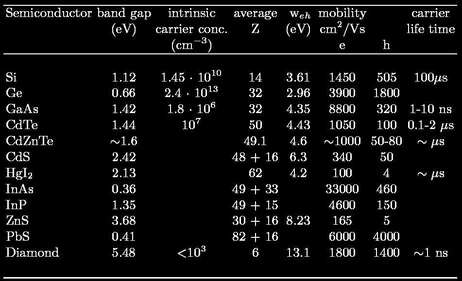
57 Metal-semiconductor junction metal semiconductor note work function Φ M depends on type of metal Φ S depends on doping χ S = electron affinity = E vac E C is independent of doping Schottky Contact =potential barrier i.e eφ S < eφ m

 N D (cm -3 ) tunneling R C (Ωcm 2 )")
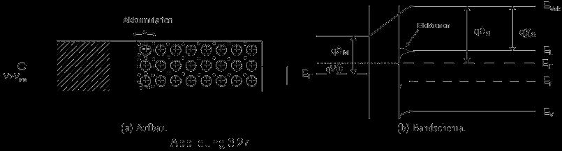
58 Metal-semiconductor junction Ohmic Contact =very thin potential barrier when E F (s.c.) E C (s.c.) N D (cm -3 ) tunneling R C (Ωcm 2 ) achieved by high doping (>10 19 cm -3 )

59 MOS structure - I

60 MOS structure II

61 End of the lecture
Chapter 1 Overview of Semiconductor Materials and Physics
 Chapter 1 Overview of Semiconductor Materials and Physics Professor Paul K. Chu Conductivity / Resistivity of Insulators, Semiconductors, and Conductors Semiconductor Elements Period II III IV V VI 2 B
Lecture 4. Detectors for Ionizing Particles
 Lecture 4 Detectors for Ionizing Particles Introduction Overview of detector systems Sources of radiation Radioactive decay Cosmic Radiation Accelerators Content Interaction of Radiation with Matter General
EECS130 Integrated Circuit Devices
 EECS130 Integrated Circuit Devices Professor Ali Javey 8/30/2007 Semiconductor Fundamentals Lecture 2 Read: Chapters 1 and 2 Last Lecture: Energy Band Diagram Conduction band E c E g Band gap E v Valence
Advantages / Disadvantages of semiconductor detectors
 Advantages / Disadvantages of semiconductor detectors Semiconductor detectors have a high density (compared to gas detector) large energy loss in a short distance diffusion effect is smaller than in gas
Basic cell design. Si cell
 Basic cell design Si cell 1 Concepts needed to describe photovoltaic device 1. energy bands in semiconductors: from bonds to bands 2. free carriers: holes and electrons, doping 3. electron and hole current:
Semiconductor Detectors
 Semiconductor Detectors Summary of Last Lecture Band structure in Solids: Conduction band Conduction band thermal conductivity: E g > 5 ev Valence band Insulator Charge carrier in conductor: e - Charge
Engineering 2000 Chapter 8 Semiconductors. ENG2000: R.I. Hornsey Semi: 1
 Engineering 2000 Chapter 8 Semiconductors ENG2000: R.I. Hornsey Semi: 1 Overview We need to know the electrical properties of Si To do this, we must also draw on some of the physical properties and we
A semiconductor is an almost insulating material, in which by contamination (doping) positive or negative charge carriers can be introduced.
 positive or negative charge carriers can be introduced.") Semiconductor A semiconductor is an almost insulating material, in which by contamination (doping) positive or negative charge carriers can be introduced. Page 2 Semiconductor materials Page 3 Energy levels
Semiconductor A semiconductor is an almost insulating material, in which by contamination (doping) positive or negative charge carriers can be introduced. Page 2 Semiconductor materials Page 3 Energy levels
Lecture 8. Detectors for Ionizing Particles
 Lecture 8 Detectors for Ionizing Particles Content Introduction Overview of detector systems Sources of radiation Radioactive decay Cosmic Radiation Accelerators Interaction of Radiation with Matter General
Introduction to Semiconductor Physics. Prof.P. Ravindran, Department of Physics, Central University of Tamil Nadu, India
 Introduction to Semiconductor Physics 1 Prof.P. Ravindran, Department of Physics, Central University of Tamil Nadu, India http://folk.uio.no/ravi/cmp2013 Review of Semiconductor Physics Semiconductor fundamentals
EECS143 Microfabrication Technology
 EECS143 Microfabrication Technology Professor Ali Javey Introduction to Materials Lecture 1 Evolution of Devices Yesterday s Transistor (1947) Today s Transistor (2006) Why Semiconductors? Conductors e.g
smal band gap Saturday, April 9, 2011
 small band gap upper (conduction) band empty small gap valence band filled 2s 2p 2s 2p hybrid (s+p)band 2p no gap 2s (depend on the crystallographic orientation) extrinsic semiconductor semi-metal electron
SEMICONDUCTOR PHYSICS
 SEMICONDUCTOR PHYSICS by Dibyendu Chowdhury Semiconductors The materials whose electrical conductivity lies between those of conductors and insulators, are known as semiconductors. Silicon Germanium Cadmium
EE143 Fall 2016 Microfabrication Technologies. Evolution of Devices
 EE143 Fall 2016 Microfabrication Technologies Prof. Ming C. Wu wu@eecs.berkeley.edu 511 Sutardja Dai Hall (SDH) 1-1 Evolution of Devices Yesterday s Transistor (1947) Today s Transistor (2006) 1-2 1 Why
Lecture 2. Semiconductor Physics. Sunday 4/10/2015 Semiconductor Physics 1-1
 Lecture 2 Semiconductor Physics Sunday 4/10/2015 Semiconductor Physics 1-1 Outline Intrinsic bond model: electrons and holes Charge carrier generation and recombination Intrinsic semiconductor Doping:
Charge Carriers in Semiconductor
 Charge Carriers in Semiconductor To understand PN junction s IV characteristics, it is important to understand charge carriers behavior in solids, how to modify carrier densities, and different mechanisms
Semiconductors. SEM and EDAX images of an integrated circuit. SEM EDAX: Si EDAX: Al. Institut für Werkstoffe der ElektrotechnikIWE
 SEM and EDAX images of an integrated circuit SEM EDAX: Si EDAX: Al source: [Cal 99 / 605] M&D-.PPT, slide: 1, 12.02.02 Classification semiconductors electronic semiconductors mixed conductors ionic conductors
Ch. 2: Energy Bands And Charge Carriers In Semiconductors
 Ch. 2: Energy Bands And Charge Carriers In Semiconductors Discrete energy levels arise from balance of attraction force between electrons and nucleus and repulsion force between electrons each electron
ECE 442. Spring, Lecture -2
 ECE 442 Power Semiconductor Devices and Integrated circuits Spring, 2006 University of Illinois at Chicago Lecture -2 Semiconductor physics band structures and charge carriers 1. What are the types of
Semiconductor-Detectors
 Semiconductor-Detectors 1 Motivation ~ 195: Discovery that pn-- junctions can be used to detect particles. Semiconductor detectors used for energy measurements ( Germanium) Since ~ 3 years: Semiconductor
EE 5344 Introduction to MEMS CHAPTER 5 Radiation Sensors
 EE 5344 Introduction to MEMS CHAPTER 5 Radiation Sensors 5. Radiation Microsensors Radiation µ-sensors convert incident radiant signals into standard electrical out put signals. Radiant Signals Classification
Chap. 11 Semiconductor Diodes
 Chap. 11 Semiconductor Diodes Semiconductor diodes provide the best resolution for energy measurements, silicon based devices are generally used for charged-particles, germanium for photons. Scintillators
Silicon Detectors in High Energy Physics
 Thomas Bergauer (HEPHY Vienna) IPM Teheran 22 May 2011 Sunday: Schedule Silicon Detectors in Semiconductor Basics (45 ) Detector concepts: Pixels and Strips (45 ) Coffee Break Strip Detector Performance
CLASS 12th. Semiconductors
 CLASS 12th Semiconductors 01. Distinction Between Metals, Insulators and Semi-Conductors Metals are good conductors of electricity, insulators do not conduct electricity, while the semiconductors have
1 Review of semiconductor materials and physics
 Part One Devices 1 Review of semiconductor materials and physics 1.1 Executive summary Semiconductor devices are fabricated using specific materials that offer the desired physical properties. There are
Lecture 2. Introduction to semiconductors Structures and characteristics in semiconductors
 Lecture 2 Introduction to semiconductors Structures and characteristics in semiconductors Semiconductor p-n junction Metal Oxide Silicon structure Semiconductor contact Literature Glen F. Knoll, Radiation
Course overview. Me: Dr Luke Wilson. The course: Physics and applications of semiconductors. Office: E17 open door policy
 Course overview Me: Dr Luke Wilson Office: E17 open door policy email: luke.wilson@sheffield.ac.uk The course: Physics and applications of semiconductors 10 lectures aim is to allow time for at least one
MTLE-6120: Advanced Electronic Properties of Materials. Intrinsic and extrinsic semiconductors. Reading: Kasap:
 MTLE-6120: Advanced Electronic Properties of Materials 1 Intrinsic and extrinsic semiconductors Reading: Kasap: 5.1-5.6 Band structure and conduction 2 Metals: partially filled band(s) i.e. bands cross
Introduction to Engineering Materials ENGR2000. Dr.Coates
 Introduction to Engineering Materials ENGR2000 Chapter 18: Electrical Properties Dr.Coates 18.2 Ohm s Law V = IR where R is the resistance of the material, V is the voltage and I is the current. l R A
Chem 481 Lecture Material 3/20/09
 Chem 481 Lecture Material 3/20/09 Radiation Detection and Measurement Semiconductor Detectors The electrons in a sample of silicon are each bound to specific silicon atoms (occupy the valence band). If
Unit IV Semiconductors Engineering Physics
 Introduction A semiconductor is a material that has a resistivity lies between that of a conductor and an insulator. The conductivity of a semiconductor material can be varied under an external electrical
Chemistry Instrumental Analysis Lecture 8. Chem 4631
 Chemistry 4631 Instrumental Analysis Lecture 8 UV to IR Components of Optical Basic components of spectroscopic instruments: stable source of radiant energy transparent container to hold sample device
Direct and Indirect Semiconductor
 Direct and Indirect Semiconductor Allowed values of energy can be plotted vs. the propagation constant, k. Since the periodicity of most lattices is different in various direction, the E-k diagram must
ECE 335: Electronic Engineering Lecture 2: Semiconductors
 Faculty of Engineering ECE 335: Electronic Engineering Lecture 2: Semiconductors Agenda Intrinsic Semiconductors Extrinsic Semiconductors N-type P-type Carrier Transport Drift Diffusion Semiconductors
Semiconductor Detectors are Ionization Chambers. Detection volume with electric field Energy deposited positive and negative charge pairs
 1 V. Semiconductor Detectors V.1. Principles Semiconductor Detectors are Ionization Chambers Detection volume with electric field Energy deposited positive and negative charge pairs Charges move in field
Radiation Detection for the Beta- Delayed Alpha and Gamma Decay of 20 Na. Ellen Simmons
 Radiation Detection for the Beta- Delayed Alpha and Gamma Decay of 20 Na Ellen Simmons 1 Contents Introduction Review of the Types of Radiation Charged Particle Radiation Detection Review of Semiconductor
3.1 Introduction to Semiconductors. Y. Baghzouz ECE Department UNLV
 3.1 Introduction to Semiconductors Y. Baghzouz ECE Department UNLV Introduction In this lecture, we will cover the basic aspects of semiconductor materials, and the physical mechanisms which are at the
Crystal Properties. MS415 Lec. 2. High performance, high current. ZnO. GaN
 Crystal Properties Crystal Lattices: Periodic arrangement of atoms Repeated unit cells (solid-state) Stuffing atoms into unit cells Determine mechanical & electrical properties High performance, high current
1 Name: Student number: DEPARTMENT OF PHYSICS AND PHYSICAL OCEANOGRAPHY MEMORIAL UNIVERSITY OF NEWFOUNDLAND. Fall :00-11:00
 1 Name: DEPARTMENT OF PHYSICS AND PHYSICAL OCEANOGRAPHY MEMORIAL UNIVERSITY OF NEWFOUNDLAND Final Exam Physics 3000 December 11, 2012 Fall 2012 9:00-11:00 INSTRUCTIONS: 1. Answer all seven (7) questions.
The Semiconductor in Equilibrium
 Lecture 6 Semiconductor physics IV The Semiconductor in Equilibrium Equilibrium, or thermal equilibrium No external forces such as voltages, electric fields. Magnetic fields, or temperature gradients are
Atoms? All matters on earth made of atoms (made up of elements or combination of elements).
.") Chapter 1 Atoms? All matters on earth made of atoms (made up of elements or combination of elements). Atomic Structure Atom is the smallest particle of an element that can exist in a stable or independent
Chapter 1 Atoms? All matters on earth made of atoms (made up of elements or combination of elements). Atomic Structure Atom is the smallest particle of an element that can exist in a stable or independent
ORTEC. Review of the Physics of Semiconductor Detectors. Interaction of Ionizing Radiation with Semiconductor Detectors. Heavy Charged Particles
 ORTEC Review of the Physics of Historically, semiconductor detectors were conceived as solid-state ionization chambers. To obtain a high-electric-field, low-current, solid-state device for detection and
Lecture 1. OUTLINE Basic Semiconductor Physics. Reading: Chapter 2.1. Semiconductors Intrinsic (undoped) silicon Doping Carrier concentrations
 silicon Doping Carrier concentrations") Lecture 1 OUTLINE Basic Semiconductor Physics Semiconductors Intrinsic (undoped) silicon Doping Carrier concentrations Reading: Chapter 2.1 EE105 Fall 2007 Lecture 1, Slide 1 What is a Semiconductor? Low
Lecture 1 OUTLINE Basic Semiconductor Physics Semiconductors Intrinsic (undoped) silicon Doping Carrier concentrations Reading: Chapter 2.1 EE105 Fall 2007 Lecture 1, Slide 1 What is a Semiconductor? Low
The interaction of radiation with matter
 Basic Detection Techniques 2009-2010 http://www.astro.rug.nl/~peletier/detectiontechniques.html Detection of energetic particles and gamma rays The interaction of radiation with matter Peter Dendooven
CHAPTER 2: ENERGY BANDS & CARRIER CONCENTRATION IN THERMAL EQUILIBRIUM. M.N.A. Halif & S.N. Sabki
 CHAPTER 2: ENERGY BANDS & CARRIER CONCENTRATION IN THERMAL EQUILIBRIUM OUTLINE 2.1 INTRODUCTION: 2.1.1 Semiconductor Materials 2.1.2 Basic Crystal Structure 2.1.3 Basic Crystal Growth technique 2.1.4 Valence
Review of Semiconductor Fundamentals
 ECE 541/ME 541 Microelectronic Fabrication Techniques Review of Semiconductor Fundamentals Zheng Yang (ERF 3017, email: yangzhen@uic.edu) Page 1 Semiconductor A semiconductor is an almost insulating material,
n N D n p = n i p N A
 Summary of electron and hole concentration in semiconductors Intrinsic semiconductor: E G n kt i = pi = N e 2 0 Donor-doped semiconductor: n N D where N D is the concentration of donor impurity Acceptor-doped
Lecture 2. Introduction to semiconductors Structures and characteristics in semiconductors
 Lecture 2 Introduction to semiconductors Structures and characteristics in semiconductors Semiconductor p-n junction Metal Oxide Silicon structure Semiconductor contact Literature Glen F. Knoll, Radiation
ECE 142: Electronic Circuits Lecture 3: Semiconductors
 Faculty of Engineering ECE 142: Electronic Circuits Lecture 3: Semiconductors Agenda Intrinsic Semiconductors Extrinsic Semiconductors N-type P-type Carrier Transport Drift Diffusion Semiconductors A semiconductor
Semiconductor Fundamentals. Professor Chee Hing Tan
 Semiconductor Fundamentals Professor Chee Hing Tan c.h.tan@sheffield.ac.uk Why use semiconductor? Microprocessor Transistors are used in logic circuits that are compact, low power consumption and affordable.
PN Junction
 P Junction 2017-05-04 Definition Power Electronics = semiconductor switches are used Analogue amplifier = high power loss 250 200 u x 150 100 u Udc i 50 0 0 50 100 150 200 250 300 350 400 i,u dc i,u u
Semiconductor X-Ray Detectors. Tobias Eggert Ketek GmbH
 Semiconductor X-Ray Detectors Tobias Eggert Ketek GmbH Semiconductor X-Ray Detectors Part A Principles of Semiconductor Detectors 1. Basic Principles 2. Typical Applications 3. Planar Technology 4. Read-out
CME 300 Properties of Materials. ANSWERS: Homework 9 November 26, As atoms approach each other in the solid state the quantized energy states:
 CME 300 Properties of Materials ANSWERS: Homework 9 November 26, 2011 As atoms approach each other in the solid state the quantized energy states: are split. This splitting is associated with the wave
Physics 663. Particle Physics Phenomenology. April 23, Physics 663, lecture 4 1
 Physics 663 Particle Physics Phenomenology April 23, 2002 Physics 663, lecture 4 1 Detectors Interaction of Charged Particles and Radiation with Matter Ionization loss of charged particles Coulomb scattering
Emphasis on what happens to emitted particle (if no nuclear reaction and MEDIUM (i.e., atomic effects)
") LECTURE 5: INTERACTION OF RADIATION WITH MATTER All radiation is detected through its interaction with matter! INTRODUCTION: What happens when radiation passes through matter? Emphasis on what happens
LECTURE 5: INTERACTION OF RADIATION WITH MATTER All radiation is detected through its interaction with matter! INTRODUCTION: What happens when radiation passes through matter? Emphasis on what happens
Semiconductors 1. Explain different types of semiconductors in detail with necessary bond diagrams. Intrinsic semiconductors:
 Semiconductors 1. Explain different types of semiconductors in detail with necessary bond diagrams. There are two types of semi conductors. 1. Intrinsic semiconductors 2. Extrinsic semiconductors Intrinsic
Nuclear Physics and Astrophysics
 Nuclear Physics and Astrophysics PHY-30 Dr. E. Rizvi Lecture 4 - Detectors Binding Energy Nuclear mass MN less than sum of nucleon masses Shows nucleus is a bound (lower energy) state for this configuration
The outline. 1) Detector parameters: efficiency, geometrical acceptance, dead-time, resolution, linearity. 2) gaseous ionization chambers
 Detector parameters: efficiency, geometrical acceptance, dead-time, resolution, linearity. 2) gaseous ionization chambers") The outline 1) Detector parameters: efficiency, geometrical acceptance, dead-time, resolution, linearity 2) gaseous ionization chambers 3) proportional counters- ionization measurement 4) silicon detectors
The outline 1) Detector parameters: efficiency, geometrical acceptance, dead-time, resolution, linearity 2) gaseous ionization chambers 3) proportional counters- ionization measurement 4) silicon detectors
Minimal Update of Solid State Physics
 Minimal Update of Solid State Physics It is expected that participants are acquainted with basics of solid state physics. Therefore here we will refresh only those aspects, which are absolutely necessary
ELECTRONIC I Lecture 1 Introduction to semiconductor. By Asst. Prof Dr. Jassim K. Hmood
 ELECTRONIC I Lecture 1 Introduction to semiconductor By Asst. Prof Dr. Jassim K. Hmood SOLID-STATE ELECTRONIC MATERIALS Electronic materials generally can be divided into three categories: insulators,
DETECTORS. I. Charged Particle Detectors
 DETECTORS I. Charged Particle Detectors A. Scintillators B. Gas Detectors 1. Ionization Chambers 2. Proportional Counters 3. Avalanche detectors 4. Geiger-Muller counters 5. Spark detectors C. Solid State
Electronic Circuits for Mechatronics ELCT 609 Lecture 2: PN Junctions (1)
") Electronic Circuits for Mechatronics ELCT 609 Lecture 2: PN Junctions (1) Assistant Professor Office: C3.315 E-mail: eman.azab@guc.edu.eg 1 Electronic (Semiconductor) Devices P-N Junctions (Diodes): Physical
Electronic Circuits for Mechatronics ELCT 609 Lecture 2: PN Junctions (1) Assistant Professor Office: C3.315 E-mail: eman.azab@guc.edu.eg 1 Electronic (Semiconductor) Devices P-N Junctions (Diodes): Physical
Solid State Physics SEMICONDUCTORS - IV. Lecture 25. A.H. Harker. Physics and Astronomy UCL
 Solid State Physics SEMICONDUCTORS - IV Lecture 25 A.H. Harker Physics and Astronomy UCL 9.9 Carrier diffusion and recombination Suppose we have a p-type semiconductor, i.e. n h >> n e. (1) Create a local
EEE4106Z Radiation Interactions & Detection
 EEE4106Z Radiation Interactions & Detection 2. Radiation Detection Dr. Steve Peterson 5.14 RW James Department of Physics University of Cape Town steve.peterson@uct.ac.za May 06, 2015 EEE4106Z :: Radiation
Introductory Nanotechnology ~ Basic Condensed Matter Physics ~
 Introductory Nanotechnology ~ Basic Condensed Matter Physics ~ Atsufumi Hirohata Department of Electronics Quick Review over the Last Lecture Classic model : Dulong-Petit empirical law c V, mol 3R 0 E
Three Most Important Topics (MIT) Today
 Today") Three Most Important Topics (MIT) Today Electrons in periodic potential Energy gap nearly free electron Bloch Theorem Energy gap tight binding Chapter 1 1 Electrons in Periodic Potential We now know the
Three Most Important Topics (MIT) Today Electrons in periodic potential Energy gap nearly free electron Bloch Theorem Energy gap tight binding Chapter 1 1 Electrons in Periodic Potential We now know the
Lecture 2 Electrons and Holes in Semiconductors
 EE 471: Transport Phenomena in Solid State Devices Spring 2018 Lecture 2 Electrons and Holes in Semiconductors Bryan Ackland Department of Electrical and Computer Engineering Stevens Institute of Technology
Electro - Principles I
 Electro - Principles I Page 10-1 Atomic Theory It is necessary to know what goes on at the atomic level of a semiconductor so the characteristics of the semiconductor can be understood. In many cases a
Electron Energy, E E = 0. Free electron. 3s Band 2p Band Overlapping energy bands. 3p 3s 2p 2s. 2s Band. Electrons. 1s ATOM SOLID.
 Electron Energy, E Free electron Vacuum level 3p 3s 2p 2s 2s Band 3s Band 2p Band Overlapping energy bands Electrons E = 0 1s ATOM 1s SOLID In a metal the various energy bands overlap to give a single
Experimental Particle Physics
 Experimental Particle Physics Particle Interactions and Detectors Lecture 2 2nd May 2014 Fergus Wilson, RAL 1/31 How do we detect particles? Particle Types Charged (e - /K - /π - ) Photons (γ) Electromagnetic
ELEMENTARY BAND THEORY
 ELEMENTARY BAND THEORY PHYSICIST Solid state band Valence band, VB Conduction band, CB Fermi energy, E F Bloch orbital, delocalized n-doping p-doping Band gap, E g Direct band gap Indirect band gap Phonon
PHYS485 Materials Physics
 5/11/017 PHYS485 Materials Physics Dr. Gregory W. Clar Manchester University LET S GO ON A (TEK)ADVENTURE! WHAT? TRIP TO A MAKER S SPACE IN FORT WAYNE WHEN? THURSDAY, MAY 11 TH @ 5PM WHERE? TEKVENTURE
Semiconductor device structures are traditionally divided into homojunction devices
 0. Introduction: Semiconductor device structures are traditionally divided into homojunction devices (devices consisting of only one type of semiconductor material) and heterojunction devices (consisting
Semiconductor Physics. Lecture 3
 Semiconductor Physics Lecture 3 Intrinsic carrier density Intrinsic carrier density Law of mass action Valid also if we add an impurity which either donates extra electrons or holes the number of carriers
ELECTRONIC DEVICES AND CIRCUITS SUMMARY
 ELECTRONIC DEVICES AND CIRCUITS SUMMARY Classification of Materials: Insulator: An insulator is a material that offers a very low level (or negligible) of conductivity when voltage is applied. Eg: Paper,
KATIHAL FİZİĞİ MNT-510
 KATIHAL FİZİĞİ MNT-510 YARIİLETKENLER Kaynaklar: Katıhal Fiziği, Prof. Dr. Mustafa Dikici, Seçkin Yayıncılık Katıhal Fiziği, Şakir Aydoğan, Nobel Yayıncılık, Physics for Computer Science Students: With
Lecture 2. Introduction to semiconductors Structures and characteristics in semiconductors. Fabrication of semiconductor sensor
 Lecture 2 Introduction to semiconductors Structures and characteristics in semiconductors Semiconductor p-n junction Metal Oxide Silicon structure Semiconductor contact Fabrication of semiconductor sensor
Chapter V: Interactions of neutrons with matter
 Chapter V: Interactions of neutrons with matter 1 Content of the chapter Introduction Interaction processes Interaction cross sections Moderation and neutrons path For more details see «Physique des Réacteurs
Lecture 18: Semiconductors - continued (Kittel Ch. 8)
") Lecture 18: Semiconductors - continued (Kittel Ch. 8) + a - Donors and acceptors J U,e e J q,e Transport of charge and energy h E J q,e J U,h Physics 460 F 2006 Lect 18 1 Outline More on concentrations
Lecture 18: Semiconductors - continued (Kittel Ch. 8) + a - Donors and acceptors J U,e e J q,e Transport of charge and energy h E J q,e J U,h Physics 460 F 2006 Lect 18 1 Outline More on concentrations
Review of Optical Properties of Materials
 Review of Optical Properties of Materials Review of optics Absorption in semiconductors: qualitative discussion Derivation of Optical Absorption Coefficient in Direct Semiconductors Photons When dealing
Semiconductor Physics Problems 2015
 Semiconductor Physics Problems 2015 Page and figure numbers refer to Semiconductor Devices Physics and Technology, 3rd edition, by SM Sze and M-K Lee 1. The purest semiconductor crystals it is possible
* motif: a single or repeated design or color
 Chapter 2. Structure A. Electronic structure vs. Geometric structure B. Clean surface vs. Adsorbate covered surface (substrate + overlayer) C. Adsorbate structure - how are the adsorbed molecules bound
Electronics The basics of semiconductor physics
 Electronics The basics of semiconductor physics Prof. Márta Rencz, Gergely Nagy BME DED September 16, 2013 The basic properties of semiconductors Semiconductors conductance is between that of conductors
Calculating Band Structure
 Calculating Band Structure Nearly free electron Assume plane wave solution for electrons Weak potential V(x) Brillouin zone edge Tight binding method Electrons in local atomic states (bound states) Interatomic
collisions of electrons. In semiconductor, in certain temperature ranges the conductivity increases rapidly by increasing temperature
 1.9. Temperature Dependence of Semiconductor Conductivity Such dependence is one most important in semiconductor. In metals, Conductivity decreases by increasing temperature due to greater frequency of
Semiconductor Devices and Circuits Fall Midterm Exam. Instructor: Dr. Dietmar Knipp, Professor of Electrical Engineering. Name: Mat. -Nr.
 Semiconductor Devices and Circuits Fall 2003 Midterm Exam Instructor: Dr. Dietmar Knipp, Professor of Electrical Engineering Name: Mat. -Nr.: Guidelines: Duration of the Midterm: 1 hour The exam is a closed
Session 6: Solid State Physics. Diode
 Session 6: Solid State Physics Diode 1 Outline A B C D E F G H I J 2 Definitions / Assumptions Homojunction: the junction is between two regions of the same material Heterojunction: the junction is between
SEMICONDUCTOR PHYSICS REVIEW BONDS,
 SEMICONDUCTOR PHYSICS REVIEW BONDS, BANDS, EFFECTIVE MASS, DRIFT, DIFFUSION, GENERATION, RECOMBINATION February 3, 2011 The University of Toledo, Department of Physics and Astronomy SSARE, PVIC Principles
Solid State Device Fundamentals
 Solid State Device Fundamentals ES 345 Lecture Course by Alexander M. Zaitsev alexander.zaitsev@csi.cuny.edu Tel: 718 982 2812 Oice 4101b 1 The ree electron model o metals The ree electron model o metals
LN 3 IDLE MIND SOLUTIONS
 IDLE MIND SOLUTIONS 1. Let us first look in most general terms at the optical properties of solids with band gaps (E g ) of less than 4 ev, semiconductors by definition. The band gap energy (E g ) can
PHYS208 P-N Junction. Olav Torheim. May 30, 2007
 1 PHYS208 P-N Junction Olav Torheim May 30, 2007 1 Intrinsic semiconductors The lower end of the conduction band is a parabola, just like in the quadratic free electron case (E = h2 k 2 2m ). The density
Chapter 2. Semiconductor Fundamentals
 hapter Semiconductor Fundamentals.0 Introduction There are altogether 9 types of natural occurring elements, of which only few types are important in semiconductor physics and technology. They are the
ECE 250 Electronic Devices 1. Electronic Device Modeling
 ECE 250 Electronic Devices 1 ECE 250 Electronic Device Modeling ECE 250 Electronic Devices 2 Introduction to Semiconductor Physics You should really take a semiconductor device physics course. We can only
CHARGED PARTICLE INTERACTIONS
 CHARGED PARTICLE INTERACTIONS Background Charged Particles Heavy charged particles Charged particles with Mass > m e α, proton, deuteron, heavy ion (e.g., C +, Fe + ), fission fragment, muon, etc. α is
Section 12: Intro to Devices
 Section 12: Intro to Devices Extensive reading materials on reserve, including Robert F. Pierret, Semiconductor Device Fundamentals Bond Model of Electrons and Holes Si Si Si Si Si Si Si Si Si Silicon
Solid State Detectors
 Solid State Detectors Most material is taken from lectures by Michael Moll/CERN and Daniela Bortoletto/Purdue and the book Semiconductor Radiation Detectors by Gerhard Lutz. In gaseous detectors, a charged
Experimental Particle Physics
 Experimental Particle Physics Particle Interactions and Detectors Lecture 2 17th February 2010 Fergus Wilson, RAL 1/31 How do we detect particles? Particle Types Charged (e - /K - /π - ) Photons (γ) Electromagnetic
Chapter 7. The pn Junction
 Chapter 7 The pn Junction Chapter 7 PN Junction PN junction can be fabricated by implanting or diffusing donors into a P-type substrate such that a layer of semiconductor is converted into N type. Converting
Metal Semiconductor Contacts
 Metal Semiconductor Contacts The investigation of rectification in metal-semiconductor contacts was first described by Braun [33-35], who discovered in 1874 the asymmetric nature of electrical conduction
Chapter 12: Semiconductors
 Chapter 12: Semiconductors Bardeen & Shottky January 30, 2017 Contents 1 Band Structure 4 2 Charge Carrier Density in Intrinsic Semiconductors. 6 3 Doping of Semiconductors 12 4 Carrier Densities in Doped