Numerical simula,on of the performance of the dye sensi,zed solar cell
|
|
|
- Kristin Briggs
- 6 years ago
- Views:
Transcription


1 I Taller de Innovación Fotovoltaica y Celdas Solares; March 8 10, 2011, CIE UNAM, Temixco. Numerical simula,on of the performance of the dye sensi,zed solar cell Julio Villanueva Cab 1,*, Elena Guillén 2, Juan Antonio Anta 2 and Gerko Oskam 1 1 Departamento de Física Aplicada, CINVESTAV IPN, Mérida, Yucatán, México 2 Departamento de Sistemas Físicos, Químicos y Naturales, Universidad Pablo de Olavide, Sevilla, Spain * Current address: Chemical & Materials Science Center, NaQonal Renewable Energy Laboratory, Golden, CO 80401, USA

2 CB E e - D*/D + h ν recombination D 0 /D + acceptor donor E redox TCO TiO 2 dye electrolyte solution I - photoelectrochemical cell porous, high surface area metal oxide film light absorption by adsorbed sensitizer molecules electron transport in solid and ion transport in solution I - 3 I - + I - I - 3
3 I Taller de Innovación Fotovoltaica y Celdas Solares; March 8 10, 2011, CIE UNAM, Temixco. Objectives Numerical tool to simulate the current-voltage curve in Dye Sensitized Solar Cells (DSSC) Make a connection with microscopic theories on transport and recombination so the model is as rigorous as possible (but not too complex!!) Make a connection with experimental techniques to obtain the relevant parameters
4 Dye solar cells: generation, transport and recombination Absorbance x light glass TCO Electron electron density electron acceptors e - e - e - ions Open circuit Short circuit ions Particles are too small for band bending Solution with ions provide shielding Electron transport is impeded by transfer to electron acceptor in the solution x steady-state measurements (Lindquist et al.): photocurrent is dominated by diffusion
5 Continuity equation n t = 1 e J R + G n is the electron density under illumination J is the current density in the film G and R are generation and recombination rates Current density J = enµ n φ + ed n µ n is the electron mobility φ is the electrical potential D is the electron diffusion coefficient Diffusion transport equation n(x,t) t = D 2 n(x,t) 2 + n(x,t) n 0 τ 0 + Γα exp( αx) = 0 flux recombination electron injection The diffusion coefficient and recombina,on term are dependent to the light intensity transport equa,on is more complex: numerical methods to model electron transport
6 D is a power law function of the light intensity, i.e, the electron density Conduction Band k 1 k -1 E F,n Valence Band Electron Transport in Porous Nanocrystalline TiO 2 Photoelectrochemical Cells F Cao, G Oskam, G J Meyer, and P C Searson J. Phys. Chem. 1996, 100, Band diagram showing trap states in the band gap. The rate constants k 1 and k -1 denote trapping and de-trapping of electrons, respectively. The Fermi energy determines which traps dominate the transport kinetics.
7 Continuity equation for electrons 1-dimensional problem (x is the distance to the substrate) n(x,t) t = G(x) + D(n) n(x,t) 0 k R (n) n(x,t) n 0 ( ) + J TCO ed GENERATION DIFFUSION n(x,t) is the total electron density RECOMBINATION CHARGE TRANSFER FROM TCO SUBSTRATE
 ε Cell (λ) exp[ ε Cell (λ) x] dλ Injection quantum yield (0 < φ inj < 1) Dye absorption")
8 n(x, t) t = G(x) + D(n) n(x,t) 0 k R (n) n(x,t) n 0 ( ) + J TCO ed λ max G(x) = φ inj I 0 λ λ min GENERATION ( ) ε Cell (λ) exp[ ε Cell (λ) x] dλ Injection quantum yield (0 < φ inj < 1) Dye absorption coefficient
 diffusion coefficient α = 0.2-0.")
9 n(x,t) t = G(x) + D(n) n(x,t) 0 k R (n) n(x,t) n 0 ( ) + J TCO ed DIFFUSION D(n) = D ref f (n) = D ref n n ref 1 α α Density-dependent (Fermi-level dependent) diffusion coefficient α = Multiple trapping mechanism g(e) = αn t k B T αe exp k B T E F (x,t) = k BT α n(x,t) ln N t
: k R = k R ref f (n) = k R ref n n ref β E F (x,t) = k B T α n(x,t) ln N t β = (1-α)/α The same as for")
10 n(x,t) t = G(x) + D(n) n(x,t) 0 k R (n) n(x,t) n 0 ( ) + J TCO ed RECOMBINATION from nanostructured film Rate constant is f(e F ): k R = k R ref f (n) = k R ref n n ref β E F (x,t) = k B T α n(x,t) ln N t β = (1-α)/α The same as for diffusion
: ref k R = k R f (V ) = k ref R exp bev kt ref k R = k R n(x) n")
11 n(x,t) t = G(x) + D(n) n(x,t) 0 k R (n) n(x,t) n 0 ( ) + J TCO ed RECOMBINATION from nanostructured film Rate is f(v): ref k R = k R f (V ) = k ref R exp bev kt ref k R = k R n(x) n ref b α b 0.5
ev k B T exp bev k B T Butler-Volmer equation b TCO 0.")
12 n(x,t) t = G(x) + D(n) n(x,t) 0 k R (n) n(x,t) n 0 ( ) + J TCO ed TCO CHARGE TRANSFER FROM TCO SUBSTRATE 0 J TCO = J TCO exp (1 b)ev k B T exp bev k B T Butler-Volmer equation b TCO 0.5
13 n(x) Electron density profile J J SC b n V 0 a V OC n d x V V = (E E 0 F F ) e = k T B αe ln n 0 V 0 n 0
14 Practical procedure J Use the experimental short-circuit current to fit either the injection yield or the dye concentration in cell Use the experimental opencircuit voltage to obtain a first estimate of the recombination constant prefactor V
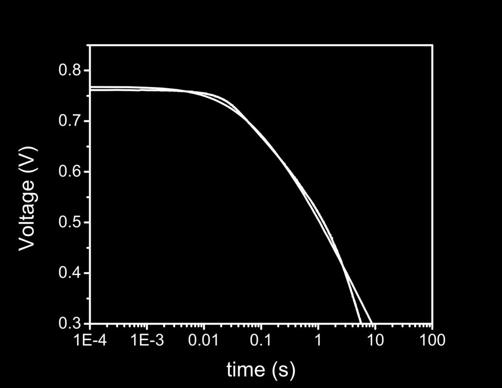
15 Use the experimental current transient to obtain the trap distribution parameter α Villanueva et al., J. Phys. Chem. C 2009, 113,
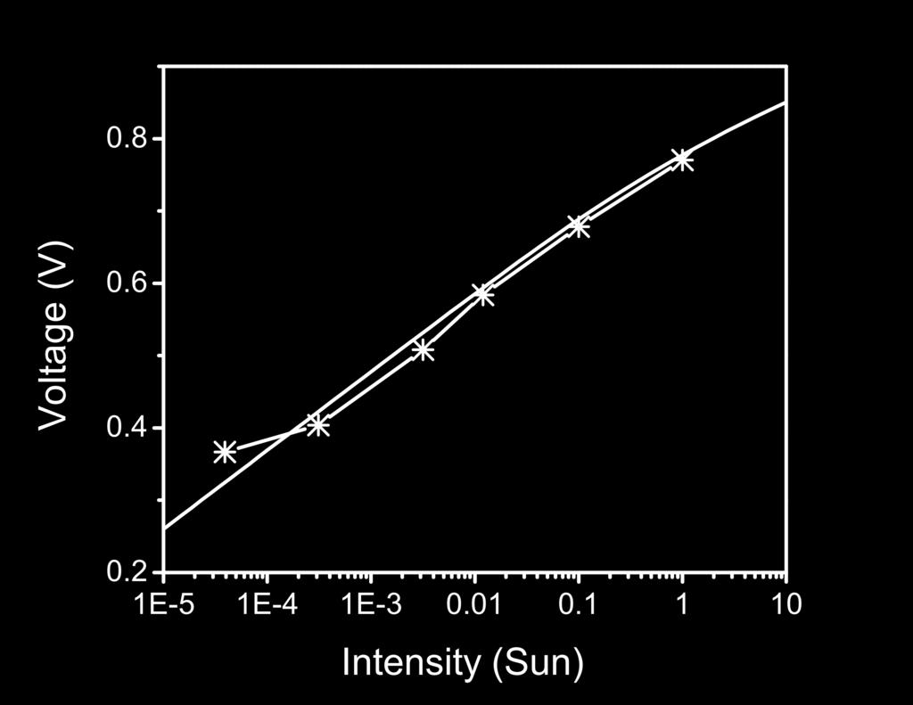
16 slope = 78 mv Use open-circuit voltage versus light intensity and time decay to obtain charge transfer parameters from TCO substrate (J 0 TCO, b)
17 J Use the current at maximum power point to obtain the total series resistance in the cell V Numerical Method: Forward Time Centered Space (FTCS) with the Lax scheme
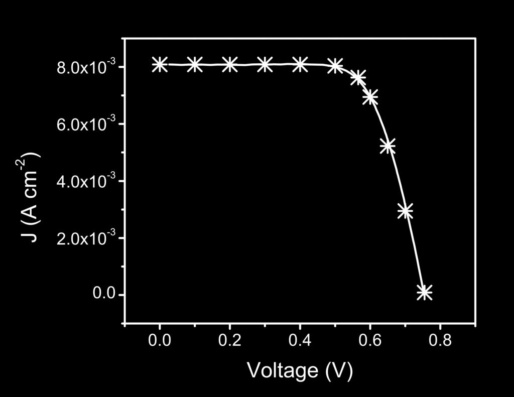
18 TiO 2 /N719/organic electrolyte ZnO/N719/solvent-free electrolyte eff = 6.5% eff = 1.5% Numerical Simulation of the Current-Voltage Curve in Dye-Sensitized Solar Cells Julio Villanueva, Juan A. Anta, Elena Guillén, and Gerko Oskam J. Phys. Chem. C 2009, 113,
19 TiO 2 (brookite)/n719/organic electrolyte α = 0.28 eff = 4.0% slope = 33 mv
20 ZnO/D149/organic solvent electrolyte eff = 2.8% R = 30 Ohm cm 2 α = 0.2 k R 0 = s -1
21 Parameter Z Cell (ZnO) T Cell (TiO 2 ) Brookite Cell ZnO/D149 C Cell (M) k 0 R (s 1 ) α blocking layer no no yes yes J 0 (TCO) (A cm 2 ) b TCO dv oc /dln(int) (mv) R (Ω cm 2 ) L (µm)
22 Transport-limited or transfer-limited recombination Model 1: Transport-limited recombination k R = k R ref n n ref 1 α α Model 2: Transfer-limited recombination k R = k ref R exp bev kt Influence of the recombination mechanism on the IV-curve of dye-sensitized solar cells J Villanueva, G Oskam and J A Anta, Solar Energy Materials & Solar Cells, 94 (2010)
23 D(n) = D ref n n ref 1 α α ref k R = k R n n ref 1 α α k R = k ref R exp bev kt V OC k BT e V OC Ln I k B T (α + b)e Ln I Model 1: Transport-limited recombination Model 2: Transfer-limited recombination
24 ZnO/D149/organic solvent electrolyte Non-ideality in Voc vs. light intensity curve γ 0.75 for NPs Model 2: Transfer-limited recombination γ = α + b α = 0.2 b = 0.55
25 Comparison total electron and free electron density models Steady-state conditions 0 = G(x) + D 2 n cb k 2 R ( n cb n 0 ) γ 0 = G(x) + D(n ) n tot tot k R (n tot ) n tot n 0 ( ) For γ = 1, both equations are formally identical Free electron Total electron If γ < 1, we have the case of non-first order recombination light intensity dependence of the electron diffusion length discrepancy results from steady-state & modulation methods Model 2: k R = k ref R exp bev kt Both models are identical with γ = α + b
26 Conclusions Numerical solution of the continuity equation in DSSC was obtained with explicit consideration of recombination via the oxide and the substrate The model can fit simultaneously current and voltage transients, open-circuit voltage vs. light intensity and the full IV curve The model was tested for several very different kind of cells and different types of recombination kinetics The total electron density model compares well with the free electron model to describe transport & recombination kinetics

27 Acknowledgements PROYECTO DE EXCELENCIA P06-FQM CONSOLIDER-INGENIO 2010 CSD FPU fellowships Grant No Y Red Temática en Fuentes de Energía
Origin and Whereabouts of Recombination in. Perovskite Solar Cells Supporting Information
 Origin and Whereabouts of Recombination in Perovskite Solar Cells Supporting Information Lidia Contreras-Bernal a, Manuel Salado a,b, Anna Todinova a, Laura Calio b, Shahzada Ahmad b, Jesús Idígoras a,
Área de Química Física, Universidad Pablo de Olavide, E-41013, Sevilla, Spain.
 Continuity Equation for the Simulation of the Current-Voltage Curve and the Time-Dependent Properties in Dye-Sensitized Solar Cells Supporting Information Juan A. Anta a, Jesús Idígoras a, Elena Guillén
Chapter 3 Modeling and Simulation of Dye-Sensitized Solar Cell
 Chapter 3 Modeling and Simulation of Dye-Sensitized Solar Cell 3.1. Introduction In recent years, dye-sensitized solar cells (DSSCs) based on nanocrystalline mesoporous TiO 2 films have attracted much
Mesoporous titanium dioxide electrolyte bulk heterojunction
 Mesoporous titanium dioxide electrolyte bulk heterojunction The term "bulk heterojunction" is used to describe a heterojunction composed of two different materials acting as electron- and a hole- transporters,
Electronic Supporting Information
 Characterization of Planar Lead Halide Perovskite Solar Cells by Impedance Spectroscopy, Open Circuit Photovoltage Decay and Intensity-Modulated Photovoltage/Photocurrent Spectroscopy Adam Pockett 1, Giles
Appendix 1: List of symbols
 Appendix 1: List of symbols Symbol Description MKS Units a Acceleration m/s 2 a 0 Bohr radius m A Area m 2 A* Richardson constant m/s A C Collector area m 2 A E Emitter area m 2 b Bimolecular recombination
FYS 3028/8028 Solar Energy and Energy Storage. Calculator with empty memory Language dictionaries
 Faculty of Science and Technology Exam in: FYS 3028/8028 Solar Energy and Energy Storage Date: 11.05.2016 Time: 9-13 Place: Åsgårdvegen 9 Approved aids: Type of sheets (sqares/lines): Number of pages incl.
e - Galvanic Cell 1. Voltage Sources 1.1 Polymer Electrolyte Membrane (PEM) Fuel Cell
 Fuel Cell") Galvanic cells convert different forms of energy (chemical fuel, sunlight, mechanical pressure, etc.) into electrical energy and heat. In this lecture, we are interested in some examples of galvanic cells.
Galvanic cells convert different forms of energy (chemical fuel, sunlight, mechanical pressure, etc.) into electrical energy and heat. In this lecture, we are interested in some examples of galvanic cells.
Supplementary Information
 Supplementary Information Supplementary Figures Supplementary Figure S1. Change in open circuit potential ( OCP) of 1% W-doped BiVO 4 photoanode upon illumination with different light intensities. Above
Classification of Solids
 Classification of Solids Classification by conductivity, which is related to the band structure: (Filled bands are shown dark; D(E) = Density of states) Class Electron Density Density of States D(E) Examples
Photovoltage phenomena in nanoscaled materials. Thomas Dittrich Hahn-Meitner-Institute Berlin
 Photovoltage phenomena in nanoscaled materials Thomas Dittrich Hahn-Meitner-Institute Berlin 1 2 Introduction From bulk to nanostructure: SPV on porous Si Retarded SPV response and its origin Photovoltage
Yixin Zhao and Kai Zhu*
 Supporting Information CH 3 NH 3 Cl-Assisted One-Step Solution Growth of CH 3 NH 3 PbI 3 : Structure, Charge- Carrier Dynamics, and Photovoltaic Properties of Perovskite Solar Cells Yixin Zhao and Kai
Supplementary Figure S1. Verifying the CH 3 NH 3 PbI 3-x Cl x sensitized TiO 2 coating UV-vis spectrum of the solution obtained by dissolving the
 Supplementary Figure S1. Verifying the CH 3 NH 3 PbI 3-x Cl x sensitized TiO 2 coating UV-vis spectrum of the solution obtained by dissolving the spiro-ometad from a perovskite-filled mesoporous TiO 2
( P ) Thales Photo-Electrochemical Techniques. Outline. Photo-Electrochemical Set-Up. Standard Solar Cell Measurements
 Thales Photo-Electrochemical Techniques. Outline. Photo-Electrochemical Set-Up. Standard Solar Cell Measurements") Outline Thales hoto-electrochemical Techniques Dynamic- and Spectral Methods for Measurements on DSSC, OSC, OLED and Electro-Chromic Devices C.-A. Schiller Standard Solar Cell Measurements Basics and the
Outline Thales hoto-electrochemical Techniques Dynamic- and Spectral Methods for Measurements on DSSC, OSC, OLED and Electro-Chromic Devices C.-A. Schiller Standard Solar Cell Measurements Basics and the
Photoelectrochemical characterization of Bi 2 S 3 thin films deposited by modified chemical bath deposition
 Indian Journal of Engineering & Materials Sciences Vol. 13, April; 2006, pp. 140-144 Photoelectrochemical characterization of Bi 2 S 3 thin films deposited by modified chemical bath deposition R R Ahire
Organic Electronic Devices
 Organic Electronic Devices Week 4: Organic Photovoltaic Devices Lecture 4.2: Characterizing Device Parameters in OPVs Bryan W. Boudouris Chemical Engineering Purdue University 1 Lecture Overview and Learning
Available online at Energy Procedia 00 (2009) Energy Procedia 2 (2010) E-MRS Spring meeting 2009, Symposium B
 Energy Procedia 2 (2010) E-MRS Spring meeting 2009, Symposium B") Available online at www.sciencedirect.com Energy Procedia 00 (2009) 000 000 Energy Procedia 2 (2010) 169 176 Energy Procedia www.elsevier.com/locate/procedia www.elsevier.com/locate/procedia E-MRS Spring
Available online at www.sciencedirect.com Energy Procedia 00 (2009) 000 000 Energy Procedia 2 (2010) 169 176 Energy Procedia www.elsevier.com/locate/procedia www.elsevier.com/locate/procedia E-MRS Spring
ZnO nanoparticle based highly efficient CdS/CdSe quantum dot-sensitized solar cells
 Electronic Supplementary Information (ESI) ZnO nanoparticle based highly efficient CdS/CdSe quantum dot-sensitized solar cells Chunhui Li, a Lei Yang, a Junyan Xiao, a Yih-Chyng Wu, Martin Søndergaard,
Solar cells operation
 Solar cells operation photovoltaic effect light and dark V characteristics effect of intensity effect of temperature efficiency efficency losses reflection recombination carrier collection and quantum
Electron Lifetime in Dye-Sensitized Solar Cells: Theory and Interpretation of Measurements
 17278 J. Phys. Chem. C 2009, 113, 17278 17290 Electron Lifetime in Dye-Sensitized Solar Cells: Theory and Interpretation of Measurements Juan Bisquert,* Francisco Fabregat-Santiago, Iván Mora-Seró, Germà
A. OTHER JUNCTIONS B. SEMICONDUCTOR HETEROJUNCTIONS -- MOLECULES AT INTERFACES: ORGANIC PHOTOVOLTAIC BULK HETEROJUNCTION DYE-SENSITIZED SOLAR CELL
 A. OTHER JUNCTIONS B. SEMICONDUCTOR HETEROJUNCTIONS -- MOLECULES AT INTERFACES: ORGANIC PHOTOVOLTAIC BULK HETEROJUNCTION DYE-SENSITIZED SOLAR CELL February 9 and 14, 2012 The University of Toledo, Department
Supplementary Figure S1. The maximum possible short circuit current (J sc ) from a solar cell versus the absorber band-gap calculated assuming 100%
 from a solar cell versus the absorber band-gap calculated assuming 100%") Supplementary Figure S1. The maximum possible short circuit current (J sc ) from a solar cell versus the absorber band-gap calculated assuming 100% (black) and 80% (red) external quantum efficiency (EQE)
Supplementary Figure S1. The maximum possible short circuit current (J sc ) from a solar cell versus the absorber band-gap calculated assuming 100% (black) and 80% (red) external quantum efficiency (EQE)
Q. Shen 1,2) and T. Toyoda 1,2)
 and T. Toyoda 1,2)") Photosensitization of nanostructured TiO 2 electrodes with CdSe quntum dots: effects of microstructure in substrates Q. Shen 1,2) and T. Toyoda 1,2) Department of Applied Physics and Chemistry 1), and
Photosensitization of nanostructured TiO 2 electrodes with CdSe quntum dots: effects of microstructure in substrates Q. Shen 1,2) and T. Toyoda 1,2) Department of Applied Physics and Chemistry 1), and
Lecture 5 Junction characterisation
 Lecture 5 Junction characterisation Jon Major October 2018 The PV research cycle Make cells Measure cells Despair Repeat 40 1.1% 4.9% Data Current density (ma/cm 2 ) 20 0-20 -1.0-0.5 0.0 0.5 1.0 Voltage
Thermionic Current Modeling and Equivalent Circuit of a III-V MQW P-I-N Photovoltaic Heterostructure
 Thermionic Current Modeling and Equivalent Circuit of a III-V MQW P-I-N Photovoltaic Heterostructure ARGYRIOS C. VARONIDES Physics and Electrical Engineering Department University of Scranton 800 Linden
A. OTHER JUNCTIONS B. SEMICONDUCTOR HETEROJUNCTIONS -- MOLECULES AT INTERFACES: ORGANIC PHOTOVOLTAIC BULK HETEROJUNCTION DYE-SENSITIZED SOLAR CELL
 A. OTHER JUNCTIONS B. SEMICONDUCTOR HETEROJUNCTIONS -- MOLECULES AT INTERFACES: ORGANIC PHOTOVOLTAIC BULK HETEROJUNCTION DYE-SENSITIZED SOLAR CELL March 24, 2015 The University of Toledo, Department of
Photovoltaic Energy Conversion. Frank Zimmermann
 Photovoltaic Energy Conversion Frank Zimmermann Solar Electricity Generation Consumes no fuel No pollution No greenhouse gases No moving parts, little or no maintenance Sunlight is plentiful & inexhaustible
Beyond the quasistatic approximation: Impedance and capacitance of an exponential distribution of traps
 PHYSICAL REVIEW B 77, 23523 28 Beyond the quasistatic approximation: Impedance and capacitance of an exponential distribution of traps Juan Bisquert* Departament de Física, Universitat Jaume I, 27 Castelló,
Conduction-Band-Offset Rule Governing J-V Distortion in CdS/CI(G)S Solar Cells
S Solar Cells") Conduction-Band-Offset Rule Governing J-V Distortion in CdS/CI(G)S Solar Cells A. Kanevce, M. Gloeckler, A.O. Pudov, and J.R. Sites Physics Department, Colorado State University, Fort Collins, CO 80523,
Conduction-Band-Offset Rule Governing J-V Distortion in CdS/CI(G)S Solar Cells A. Kanevce, M. Gloeckler, A.O. Pudov, and J.R. Sites Physics Department, Colorado State University, Fort Collins, CO 80523,
Characterization of nanostructured hybrid and organic solar cells by impedance spectroscopyw
 PCCP Dynamic Article Links View Online Cite this: DOI: 10.1039/c0cp02249g www.rsc.org/pccp PERSPECTIVE Characterization of nanostructured hybrid and organic solar cells by impedance spectroscopyw Francisco
Photovoltaic cell and module physics and technology
 Photovoltaic cell and module physics and technology Vitezslav Benda, Prof Czech Technical University in Prague benda@fel.cvut.cz www.fel.cvut.cz 6/21/2012 1 Outlines Photovoltaic Effect Photovoltaic cell
A. OTHER JUNCTIONS B. SEMICONDUCTOR HETEROJUNCTIONS -- MOLECULES AT INTERFACES: ORGANIC PHOTOVOLTAIC BULK HETEROJUNCTION DYE-SENSITIZED SOLAR CELL
 A. OTHER JUNCTIONS B. SEMICONDUCTOR HETEROJUNCTIONS -- MOLECULES AT INTERFACES: ORGANIC PHOTOVOLTAIC BULK HETEROJUNCTION DYE-SENSITIZED SOLAR CELL March 20, 2014 The University of Toledo, Department of
Organic Solar Cells. All Organic solar cell. Dye-sensitized solar cell. Dye. τ inj. τ c. τ r surface states D*/D + V o I 3 D/D.
 The 4th U.S.-Korea NanoForum April 26-27, 2007, Honolulu, USA Improvement of Device Efficiency in Conjugated Polymer/Fullerene NanoComposite Solar Cells School of Semiconductor & Chemical Engineering *
EE 5611 Introduction to Microelectronic Technologies Fall Tuesday, September 23, 2014 Lecture 07
 EE 5611 Introduction to Microelectronic Technologies Fall 2014 Tuesday, September 23, 2014 Lecture 07 1 Introduction to Solar Cells Topics to be covered: Solar cells and sun light Review on semiconductor
Session 5: Solid State Physics. Charge Mobility Drift Diffusion Recombination-Generation
 Session 5: Solid State Physics Charge Mobility Drift Diffusion Recombination-Generation 1 Outline A B C D E F G H I J 2 Mobile Charge Carriers in Semiconductors Three primary types of carrier action occur
ESE 372 / Spring 2013 / Lecture 5 Metal Oxide Semiconductor Field Effect Transistor
 Metal Oxide Semiconductor Field Effect Transistor V G V G 1 Metal Oxide Semiconductor Field Effect Transistor We will need to understand how this current flows through Si What is electric current? 2 Back
Photovoltaic cell and module physics and technology. Vitezslav Benda, Prof Czech Technical University in Prague
 Photovoltaic cell and module physics and technology Vitezslav Benda, Prof Czech Technical University in Prague benda@fel.cvut.cz www.fel.cvut.cz 1 Outlines Photovoltaic Effect Photovoltaic cell structure
Charge Carriers in Semiconductor
 Charge Carriers in Semiconductor To understand PN junction s IV characteristics, it is important to understand charge carriers behavior in solids, how to modify carrier densities, and different mechanisms
The 5 basic equations of semiconductor device physics: We will in general be faced with finding 5 quantities:
 6.012 - Electronic Devices and Circuits Solving the 5 basic equations - 2/12/08 Version The 5 basic equations of semiconductor device physics: We will in general be faced with finding 5 quantities: n(x,t),
Basic Limitations to Third generation PV performance
 Basic Limitations to Third generation PV performance Pabitra K. Nayak Weizmann Institute of Science, Rehovot, Israel THANKS to my COLLEAGUES Lee Barnea and David Cahen. Weizmann Institute of Science Juan
Solid State Dye Solar Cells: Development of Photoanode Architecture for Conversion Efficiency Improvement
 Università degli Studi di Ferrara Solid State Dye Solar Cells: Development of Photoanode Architecture for Conversion Efficiency Improvement Internal supervisor: Vincenzo Guidi External supervisor: Giampiero
Role of Cobalt Iron (Oxy)Hydroxide (CoFeO x ) as Oxygen Evolution Catalyst on Hematite Photoanodes
Hydroxide (CoFeO x ) as Oxygen Evolution Catalyst on Hematite Photoanodes") Electronic Supplementary Material (ESI) for Energy & Environmental Science. This journal is The Royal Society of Chemistry 2018 Supporting Information Role of Cobalt Iron (Oxy)Hydroxide (CoFeO x ) as Oxygen
Electronic Supplementary Material (ESI) for Energy & Environmental Science. This journal is The Royal Society of Chemistry 2018 Supporting Information Role of Cobalt Iron (Oxy)Hydroxide (CoFeO x ) as Oxygen
Solar Cell Physics: recombination and generation
 NCN Summer School: July 2011 Solar Cell Physics: recombination and generation Prof. Mark Lundstrom lundstro@purdue.edu Electrical and Computer Engineering Purdue University West Lafayette, Indiana USA
Transparent TiO 2 nanotube/nanowire arrays on TCO coated glass substrates: Synthesis and application to solar energy conversion
 Transparent TiO 2 nanotube/nanowire arrays on TCO coated glass substrates: Synthesis and application to solar energy conversion Craig A. Grimes Department of Electrical Engineering Center for Solar Nanomaterials
1 Name: Student number: DEPARTMENT OF PHYSICS AND PHYSICAL OCEANOGRAPHY MEMORIAL UNIVERSITY OF NEWFOUNDLAND. Fall :00-11:00
 1 Name: DEPARTMENT OF PHYSICS AND PHYSICAL OCEANOGRAPHY MEMORIAL UNIVERSITY OF NEWFOUNDLAND Final Exam Physics 3000 December 11, 2012 Fall 2012 9:00-11:00 INSTRUCTIONS: 1. Answer all seven (7) questions.
Supporting information. Supramolecular Halogen Bond Passivation of Organometal-Halide Perovskite Solar Cells
 Supporting information Supramolecular Halogen Bond Passivation of Organometal-Halide Perovskite Solar Cells Antonio Abate, a Michael Saliba, a Derek J. Hollman, a Samuel D. Stranks, a K. Wojciechowski,
Session 6: Solid State Physics. Diode
 Session 6: Solid State Physics Diode 1 Outline A B C D E F G H I J 2 Definitions / Assumptions Homojunction: the junction is between two regions of the same material Heterojunction: the junction is between
Semiconductor Physics Problems 2015
 Semiconductor Physics Problems 2015 Page and figure numbers refer to Semiconductor Devices Physics and Technology, 3rd edition, by SM Sze and M-K Lee 1. The purest semiconductor crystals it is possible
Chalcogenide semiconductor research and applications. Tutorial 2: Thin film characterization. Rafael Jaramillo Massachusetts Institute of Technology
 Chalcogenide semiconductor research and applications Tutorial 2: Thin film characterization Rafael Jaramillo Massachusetts Institute of Technology Section 1: Measuring composition August 20, 2017 Jaramillo
Ambient air processed mixed-ion perovskite for high efficiency solar cells
 Electronic Supplementary Material (ESI) for Journal of Materials Chemistry A. This journal is The Royal Society of Chemistry 2016 Ambient air processed mixed-ion perovskite for high efficiency solar cells
Optimization of the Properties of the Back Surface Field of a Cu(In,Ga)Se 2 Thin Film Solar Cell
Se 2 Thin Film Solar Cell") American Journal of Energy Research, 2017, Vol. 5, No. 2, 57-62 Available online at http://pubs.sciepub.com/ajer/5/2/5 Science and Education Publishing DOI:10.12691/ajer-5-2-5 Optimization of the Properties
American Journal of Energy Research, 2017, Vol. 5, No. 2, 57-62 Available online at http://pubs.sciepub.com/ajer/5/2/5 Science and Education Publishing DOI:10.12691/ajer-5-2-5 Optimization of the Properties
Theory of Electrical Characterization of Semiconductors
 Theory of Electrical Characterization of Semiconductors P. Stallinga Universidade do Algarve U.C.E.H. A.D.E.E.C. OptoElectronics SELOA Summer School May 2000, Bologna (It) Overview Devices: bulk Schottky
PERFORMANCE OF NANO STRUCTURED DYE-SENSITIZED SOLAR CELL UTILIZING NATURAL SENSITIZER OPERATED WITH PLATINUM AND CARBON COATED COUNTER ELECTRODES
 Digest Journal of Nanomaterials and Biostructures Vol. 4, No. 4, December 2009, p. 723-727 PERFORMANCE OF NANO STRUCTURED DYE-SENSITIZED SOLAR CELL UTILIZING NATURAL SENSITIZER OPERATED WITH PLATINUM AND
MODELING THE FUNDAMENTAL LIMIT ON CONVERSION EFFICIENCY OF QD SOLAR CELLS
 MODELING THE FUNDAMENTAL LIMIT ON CONVERSION EFFICIENCY OF QD SOLAR CELLS Ա.Մ.Կեչիյանց Ara Kechiantz Institute of Radiophysics and Electronics (IRPhE), National Academy of Sciences (Yerevan, Armenia) Marseille
Electric Field--Definition. Brownian motion and drift velocity
 Electric Field--Definition Definition of electrostatic (electrical) potential, energy diagram and how to remember (visualize) relationships E x Electrons roll downhill (this is a definition ) Holes are
Stability of Organic Materials. Anders Hagfeldt Dept. of Physical Chemistry Ångström Solar Center Uppsala University
 Stability of Organic Materials Anders Hagfeldt Dept. of Physical Chemistry Ångström Solar Center Uppsala University Anders.Hagfeldt@fki.uu.se Specific features of DSC Charge separation and transport are
Plastic Electronics. Joaquim Puigdollers.
 Plastic Electronics Joaquim Puigdollers Joaquim.puigdollers@upc.edu Nobel Prize Chemistry 2000 Origins Technological Interest First products.. MONOCROMATIC PHILIPS Today Future Technological interest Low
Chapter-II CHEMISTRY OF PHOTOELECTRODE- ELECTROLYTE INTERFACE
 z Chapter-II CHEMISTRY OF PHOTOELECTRODE- ELECTROLYTE INTERFACE 2.1 Introduction In recent years, semiconductor-electrolyte cells have been attracting a great deal of interest in the field of solar energy
SEMICONDUCTOR PHYSICS REVIEW BONDS,
 SEMICONDUCTOR PHYSICS REVIEW BONDS, BANDS, EFFECTIVE MASS, DRIFT, DIFFUSION, GENERATION, RECOMBINATION February 3, 2011 The University of Toledo, Department of Physics and Astronomy SSARE, PVIC Principles
Electrochemistry of Semiconductors
 Electrochemistry of Semiconductors Adrian W. Bott, Ph.D. Bioanalytical Systems, Inc. 2701 Kent Avenue West Lafayette, IN 47906-1382 This article is an introduction to the electrochemical properties of
Chapter 7. The pn Junction
 Chapter 7 The pn Junction Chapter 7 PN Junction PN junction can be fabricated by implanting or diffusing donors into a P-type substrate such that a layer of semiconductor is converted into N type. Converting
Planar Organic Photovoltaic Device. Saiful I. Khondaker
 Planar Organic Photovoltaic Device Saiful I. Khondaker Nanoscience Technology Center and Department of Physics University of Central Florida http://www.physics.ucf.edu/~khondaker W Metal 1 L ch Metal 2
February 1, 2011 The University of Toledo, Department of Physics and Astronomy SSARE, PVIC
 FUNDAMENTAL PROPERTIES OF SOLAR CELLS February 1, 2011 The University of Toledo, Department of Physics and Astronomy SSARE, PVIC Principles and Varieties of Solar Energy (PHYS 4400) and Fundamentals of
Dielectric Properties of Composite Films Made from Tin(IV) Oxide and Magnesium Oxide
 Oxide and Magnesium Oxide") OUSL Journal (2014) Vol 7, (pp67-75) Dielectric Properties of Composite Films Made from Tin(IV) Oxide and Magnesium Oxide C. N. Nupearachchi* and V. P. S. Perera Department of Physics, The Open University
OUSL Journal (2014) Vol 7, (pp67-75) Dielectric Properties of Composite Films Made from Tin(IV) Oxide and Magnesium Oxide C. N. Nupearachchi* and V. P. S. Perera Department of Physics, The Open University
Supplementary Information for:
 Supplementary Information for: In-situ measurement of electric-field screening in hysteresis-free PTAA/ FA.83 Cs.7 Pb(I.83 Br.7 ) 3 /C6 perovskite solar cells gives an ion mobility of ~3 x -7 cm /Vs; to
Demystifying Transmission Lines: What are They? Why are They Useful?
 Demystifying Transmission Lines: What are They? Why are They Useful? Purpose of This Note This application note discusses theory and practice of transmission lines. It outlines the necessity of transmission
Novel High-Efficiency Crystalline-Si-Based Compound. Heterojunction Solar Cells: HCT (Heterojunction with Compound. Thin-layer)
") Electronic Supplementary Material (ESI) for Physical Chemistry Chemical Physics. This journal is the Owner Societies 2014 Supplementary Information for Novel High-Efficiency Crystalline-Si-Based Compound
Electronic Supplementary Material (ESI) for Physical Chemistry Chemical Physics. This journal is the Owner Societies 2014 Supplementary Information for Novel High-Efficiency Crystalline-Si-Based Compound
Semiconductor Device Physics
 1 Semiconductor Device Physics Lecture 3 http://zitompul.wordpress.com 2 0 1 3 Semiconductor Device Physics 2 Three primary types of carrier action occur inside a semiconductor: Drift: charged particle
Electrochemical Cell - Basics
 Electrochemical Cell - Basics The electrochemical cell e - (a) Load (b) Load e - M + M + Negative electrode Positive electrode Negative electrode Positive electrode Cathode Anode Anode Cathode Anode Anode
Electronic Supporting Information
 Electronic Supplementary Material (ESI) for Energy & Environmental Science. This journal is The Royal Society of Chemistry 2015 Electronic Supporting Information Extracting Large photovoltages from a-sic
PHOTOVOLTAICS Fundamentals
 PHOTOVOLTAICS Fundamentals PV FUNDAMENTALS Semiconductor basics pn junction Solar cell operation Design of silicon solar cell SEMICONDUCTOR BASICS Allowed energy bands Valence and conduction band Fermi
Electrochemical deposition of metals onto silicon
 J. Phys. D: Appl. Phys. 31 (1998) 1927 1949. Printed in the UK PII: S0022-3727(98)78690-5 REVIEW ARTICLE Electrochemical deposition of metals onto silicon G Oskam, J G Long, A Natarajan and P C Searson
Excess carriers: extra carriers of values that exist at thermal equilibrium
 Ch. 4: Excess carriers In Semiconductors Excess carriers: extra carriers of values that exist at thermal equilibrium Excess carriers can be created by many methods. In this chapter the optical absorption
n N D n p = n i p N A
 Summary of electron and hole concentration in semiconductors Intrinsic semiconductor: E G n kt i = pi = N e 2 0 Donor-doped semiconductor: n N D where N D is the concentration of donor impurity Acceptor-doped
The Meaning of Fermi-Level And Related Concepts (Like Band-Bending)
") The Meaning of Fermi-Level And Related Concepts (Like Band-Bending) Martin Peckerar January 14, 2003 The Fermi level is a term derived from statistical mechanics and used to calculate the number of mobile
The Meaning of Fermi-Level And Related Concepts (Like Band-Bending) Martin Peckerar January 14, 2003 The Fermi level is a term derived from statistical mechanics and used to calculate the number of mobile
Electron transfer optimisation in organic solar cells
 Electron transfer optimisation in organic solar cells James Durrant Centre for Electronic Materials and Devices Departments of Chemistry Imperial College London Introductory remarks Charge recombination
DEVICE CHARACTERIZATION OF (AgCu)(InGa)Se 2 SOLAR CELLS
(InGa)Se 2 SOLAR CELLS") DEVICE CHARACTERIZATION OF (AgCu)(InGa)Se 2 SOLAR CELLS William Shafarman 1, Christopher Thompson 1, Jonathan Boyle 1, Gregory Hanket 1, Peter Erslev 2, J. David Cohen 2 1 Institute of Energy Conversion,
DEVICE CHARACTERIZATION OF (AgCu)(InGa)Se 2 SOLAR CELLS William Shafarman 1, Christopher Thompson 1, Jonathan Boyle 1, Gregory Hanket 1, Peter Erslev 2, J. David Cohen 2 1 Institute of Energy Conversion,
PHYS208 p-n junction. January 15, 2010
 1 PHYS208 p-n junction January 15, 2010 List of topics (1) Density of states Fermi-Dirac distribution Law of mass action Doped semiconductors Dopinglevel p-n-junctions 1 Intrinsic semiconductors List of
Chapter 1 Overview of Semiconductor Materials and Physics
 Chapter 1 Overview of Semiconductor Materials and Physics Professor Paul K. Chu Conductivity / Resistivity of Insulators, Semiconductors, and Conductors Semiconductor Elements Period II III IV V VI 2 B
OPTI510R: Photonics. Khanh Kieu College of Optical Sciences, University of Arizona Meinel building R.626
 OPTI510R: Photonics Khanh Kieu College of Optical Sciences, University of Arizona kkieu@optics.arizona.edu Meinel building R.626 Announcements Homework #6 is assigned, due May 1 st Final exam May 8, 10:30-12:30pm
Carrier Recombination
 Notes for ECE-606: Spring 013 Carrier Recombination Professor Mark Lundstrom Electrical and Computer Engineering Purdue University, West Lafayette, IN USA lundstro@purdue.edu /19/13 1 carrier recombination-generation
Holes (10x larger). Diode currents proportional to minority carrier densities on each side of the depletion region: J n n p0 = n i 2
. Diode currents proportional to minority carrier densities on each side of the depletion region: J n n p0 = n i 2") Part V. (40 pts.) A diode is composed of an abrupt PN junction with N D = 10 16 /cm 3 and N A =10 17 /cm 3. The diode is very long so you can assume the ends are at x =positive and negative infinity. 1.
Part V. (40 pts.) A diode is composed of an abrupt PN junction with N D = 10 16 /cm 3 and N A =10 17 /cm 3. The diode is very long so you can assume the ends are at x =positive and negative infinity. 1.
BJT - Mode of Operations
 JT - Mode of Operations JTs can be modeled by two back-to-back diodes. N+ P N- N+ JTs are operated in four modes. HO #6: LN 251 - JT M Models Page 1 1) Forward active / normal junction forward biased junction
Effect of TiO 2 graphene nanocomposite photoanode on dye-sensitized solar cell performance
 Bull. Mater. Sci., Vol. 38, No. 5, September 2015, pp. 1177 1182. Indian Academy of Sciences. Effect of TiO 2 graphene nanocomposite photoanode on dye-sensitized solar cell performance AKBAR ESHAGHI* and
Chapter 7. Solar Cell
 Chapter 7 Solar Cell 7.0 Introduction Solar cells are useful for both space and terrestrial application. Solar cells furnish the long duration power supply for satellites. It converts sunlight directly
Lecture 2 Solar Cell theory: pn junctions under Illumination Homojunctions Open-circuit voltage, short-circuit current, fill factor, IV curve,
 Lecture 2 Solar Cell theory: pn junctions under Illumination Homojunctions Open-circuit voltage, short-circuit current, fill factor, IV curve, Solar-toelectric Conversion Efficiency Carrier Generation
ECE-305: Spring 2018 Exam 2 Review
 ECE-305: Spring 018 Exam Review Pierret, Semiconductor Device Fundamentals (SDF) Chapter 3 (pp. 75-138) Chapter 5 (pp. 195-6) Professor Peter Bermel Electrical and Computer Engineering Purdue University,
Solar Cell Materials and Device Characterization
 Solar Cell Materials and Device Characterization April 3, 2012 The University of Toledo, Department of Physics and Astronomy SSARE, PVIC Principles and Varieties of Solar Energy (PHYS 4400) and Fundamentals
DETECTION OF PHOSGENE BY USING TiO 2 /INDICATOR NANOCRYSTALLINE THIN FILMS
 10th International Conference on Composite Science and Technology ICCST/10 A.L. Araújo, J.R. Correia, C.M. Mota Soares, et al. (Editors) IDMEC 2015 DETECTION OF PHOSGENE BY USING TiO 2 /INDICATOR NANOCRYSTALLINE
Monolithic Cells for Solar Fuels
 Electronic Supplementary Material (ESI) for Chemical Society Reviews. This journal is The Royal Society of Chemistry 2014 Monolithic Cells for Solar Fuels Jan Rongé, Tom Bosserez, David Martel, Carlo Nervi,
( )! N D ( x) ) and equilibrium
! N D ( x) ) and equilibrium") ECE 66: SOLUTIONS: ECE 66 Homework Week 8 Mark Lundstrom March 7, 13 1) The doping profile for an n- type silicon wafer ( N D = 1 15 cm - 3 ) with a heavily doped thin layer at the surface (surface concentration,
ECE 66: SOLUTIONS: ECE 66 Homework Week 8 Mark Lundstrom March 7, 13 1) The doping profile for an n- type silicon wafer ( N D = 1 15 cm - 3 ) with a heavily doped thin layer at the surface (surface concentration,
Investigation on the influences of layer structure and nanoporosity of light scattering TiO 2. layer in DSSC. Journal of Physics: Conference Series
 Journal of Physics: Conference Series PAPER OPEN ACCESS Investigation on the influences of layer structure and nanoporosity of light scattering TiO layer in DSSC To cite this article: T Apriani et al 1
Optical and Electrical Modeling of Three Dimensional Dye-Sensitized Solar Cells
 Optical and Electrical Modeling of Three Dimensional Dye-Sensitized Solar Cells Peijun Guo *1, Shi Qiang Li 1, Nanjia Zhou 1, Jie Zhang 2, Robert P.H. Chang 1 1 Northwestern University, 2 Zhejiang University
The Role of doping in the window layer on Performance of a InP Solar Cells USING AMPS-1D
 IOSR Journal of Engineering (IOSRJEN) ISSN: 2250-3021 Volume 2, Issue 8(August 2012), PP 42-46 The Role of doping in the window layer on Performance of a InP Solar Cells USING AMPS-1D Dennai Benmoussa
Silicon solar cells: basics of simulation and modelling
 Silicon solar cells: basics of simulation and modelling Using the mathematical program Maple to simulate and model a silicon solar cell Kisel solceller: Grunderna för simulering och modellering Sebastian
Section 12: Intro to Devices
 Section 12: Intro to Devices Extensive reading materials on reserve, including Robert F. Pierret, Semiconductor Device Fundamentals Bond Model of Electrons and Holes Si Si Si Si Si Si Si Si Si Silicon
Laser Induced Control of Condensed Phase Electron Transfer
 Laser Induced Control of Condensed Phase Electron Transfer Rob D. Coalson, Dept. of Chemistry, Univ. of Pittsburgh Yuri Dakhnovskii, Dept. of Physics, Univ. of Wyoming Deborah G. Evans, Dept. of Chemistry,
Deliverable D1.3 Demonstration of patterning processes allowing to
 D.3 H2020-LCE-205- CHEOPS Production technology to achieve low Cost and Highly Efficient photovoltaic Perovskite Solar cells Deliverable D.3 WP Perovskite single junction development Authors: Soo-Jin Moon
Electronic Supplementary Information. Recombination kinetics in silicon solar cell under low-concentration: Electroanalytical
 Electronic Supplementary Material (ESI) for Physical Chemistry Chemical Physics. This journal is the Owner Societies 2014 Electronic Supplementary Information Recombination kinetics in silicon solar cell
Mikaël Cugnet, Issam Baghdadi, and Marion Perrin OCTOBER 10, Excerpt from the Proceedings of the 2012 COMSOL Conference in Milan
 Mikaël Cugnet, Issam Baghdadi, and Marion Perrin OCTOBER 0, 202 Comsol Conference Europe 202, Milan, CEA Italy 0 AVRIL 202 PAGE Excerpt from the Proceedings of the 202 COMSOL Conference in Milan SUMMARY