Lecture 2 Solar Cell theory: pn junctions under Illumination Homojunctions Open-circuit voltage, short-circuit current, fill factor, IV curve,
|
|
|
- Jodie Wright
- 6 years ago
- Views:
Transcription
1 Lecture 2 Solar Cell theory: pn junctions under Illumination Homojunctions Open-circuit voltage, short-circuit current, fill factor, IV curve, Solar-toelectric Conversion Efficiency Carrier Generation and recombination Defects and Minority carrier diffusion Solutions to the diffusion equation under spatially-homgeneous and Inhomogeneous generation Heterojunctions
2

3 Celdas Solares
4
 EL MATERIAL DE CONSTRUCCION DE CELDA SOLAR SE")
5 LA TECNOLOGIA FOTOVOLTAICA ESTA CONTEMPLADA PARA APLICACIÓN AUTONAMA. ELECTRIFICACION RURAL, BOMBEO DE AGUA, ILUMINACION DE CARRATERAS, MONITOREO DE NIVELS DE AGUA EN RIOS ETC. SON ALGUNOS EJEMPLOS ESTA TECNOLOGIA CONVIERTE LA ENERGIA SOLAR DIRECTO A ENERGIA ELECTRICA DC UTILIZABDO MODULOS FOTOVOLTAICOS (CELDAS SOLARES) EL MATERIAL DE CONSTRUCCION DE CELDA SOLAR SE LLAMA SEMICONDUCTOR

6

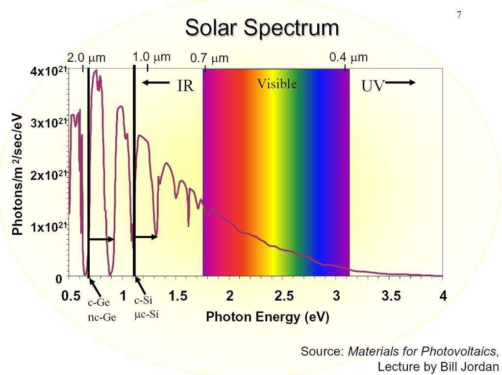
7
8
9
10
11

12

13


14 Example: PV-Roof and Front, Clemson Summer School Dr. Karl Molter / FH Trier / molter@fhtrier.de 14

15 Alwitra Solar-foil Clemson Summer School Dr. Karl Molter / FH Trier / molter@fhtrier.de 15

16 Example: Sports-Center Tübingen Clemson Summer School Dr. Karl Molter / FH Trier / molter@fhtrier.de 16

17 Example: Fire-brigade Clemson Summer School Dr. Karl Molter / FH Trier / molter@fhtrier.de 17

18 Example: BP Showcase Clemson Summer School Dr. Karl Molter / FH Trier / molter@fhtrier.de 18

 Higher cost and better space utilization Most often manufactured in")
19 Crystalline Silicon Polycrystalline Si Made from melting Si into ingots, slicing off wafers Cell efficiencies of 14% - 15% Widest use Monocrystalline Si Grown crystals, more uniform structure Higher cell efficiencies (17% - 22%) Higher cost and better space utilization Most often manufactured in framed modules

20 Amorphous Thin-Film Si Si solution layered onto various substrates Conversion efficiencies of 9% to 12% Some framed module products, others bonded to flexible roofing materials Very uniform appearance, but less effective space utilization Less costly to produce than crystalline modules


21 Building Integrated PV Roof tile replacements Solar glass Thin film bonded to single-ply membrane roofing material

22 Solar-roof shingle Clemson Summer School Dr. Karl Molter / FH Trier / molter@fhtrier.de 22
23

24 25 m2

25
26 300 m2
27
28
 Tracking mirrors focus sunlight on stationary Si (Energy Innovations Sunflower )")
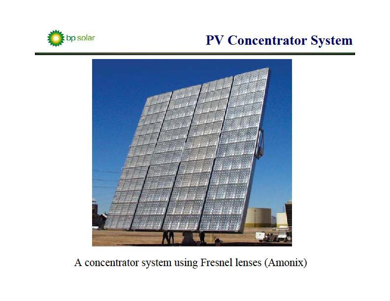
29 Concentrating Solar Panels Fresnel lenses in tracking panels concentrate light 500:1 on smaller amount of Si (Xerox PARC Research) Tracking mirrors focus sunlight on stationary Si (Energy Innovations Sunflower )
30 History 1839: Discovery of the photoelectric effect by Bequerel 1873: Discovery of the photoelectric effect of Selen (change of electrical resistance) 1954: First Silicon Solar Cell as a result of the upcoming semiconductor technology ( = 5 %) Clemson Summer School Dr. Karl Molter / FH Trier / molter@fhtrier.de 30
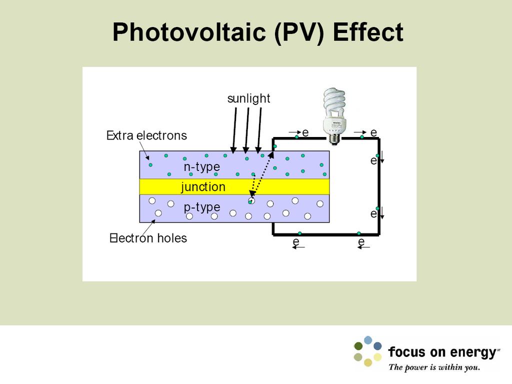
31 Energía Fotovoltaica Efecto Fotovoltaico LUZ SOLAR El Efecto Fotovoltaico (FV): es la generación de un voltaje en las terminales de un captador solar cuando éste es iluminado. Si a las terminales del captador se le conecta un aparato eléctrico, por ejemplo, un foco, entonces el foco se enciende debido a la corriente eléctrica que circula por él. Esta es la evidencia física del fenómeno fotovoltaico. CELDA SOLAR Voltaje fotogenerado Corriente eléctrica fotogenerada

32
33 pn junction physics
34 electron-energy energy-states in solids: energy absorption and emission conduction-band - x - E F h + x + h Generation Recombination valence-band Clemson Summer School Dr. Karl Molter / FH Trier / molter@fhtrier.de 34
35 doping of semiconductors In order to avoid recombination of photo-induced charges and to extract their energy to an electric-device we need a kind of internal barrier. This can be achieved by doping of semiconductors: Doping means in this case the replacement of original atoms of the semiconductor by different ones (with slightly different electron configuration). Semiconductors like Silicon have four covalent electrons, doping is done e.g. with Boron or Phosphorus: 5 IIIB IVB VB B Si P Clemson Summer School Dr. Karl Molter / FH Trier / molter@fhtrier.de 35
36 N - Doping crystal view energy-band view conduction-band Si Si - Si Si P + - Si Si E F P + P + P + P + P + majority carriers Donator level Si Si Si n-conducting Silicon valence-band Clemson Summer School Dr. Karl Molter / FH Trier / molter@fhtrier.de 36
37 P - Doping crystal energy-band view conduction band Si Si + Si Si Si B - + Si Si Si Si E F Acceptor level B - B - B - B - B majority carriers p-conducting Silicon valence-band Clemson Summer School Dr. Karl Molter / FH Trier / molter@fhtrier.de 37
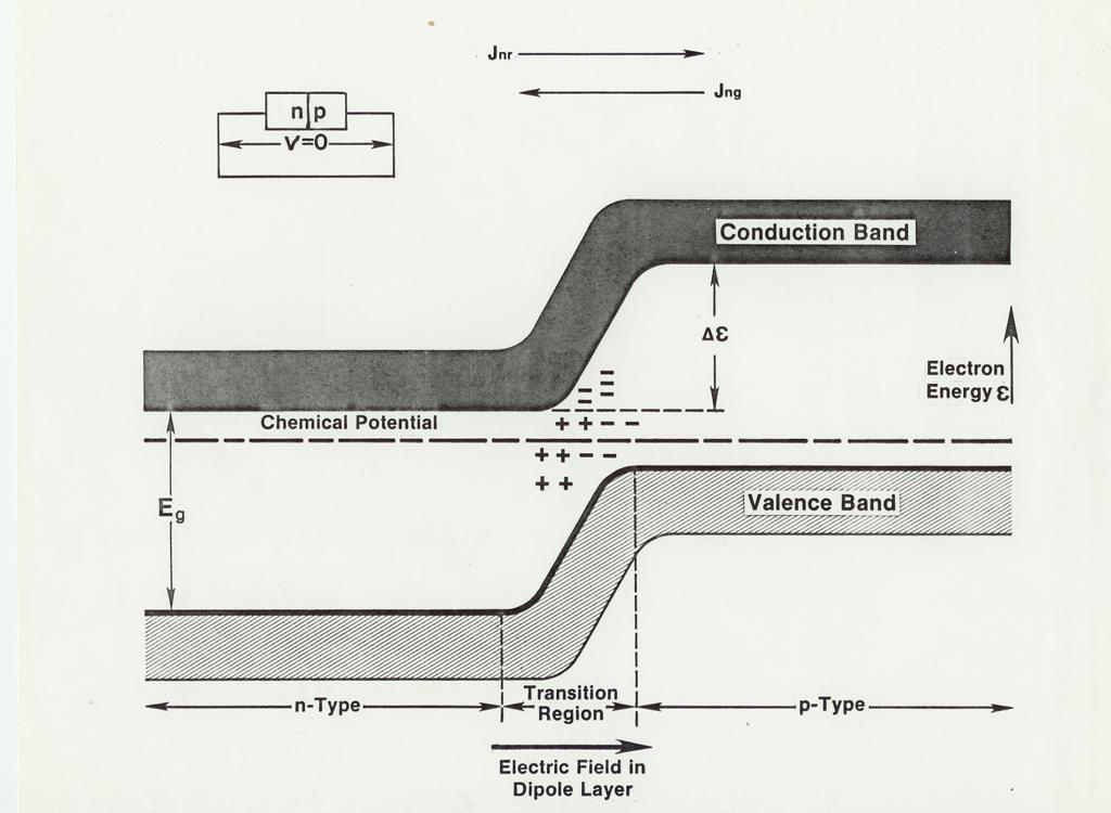
38 p/n-junction without light Band pattern view depletion-zone U d P + P + P + P + P + - Diffusion - B - B - B - B - B - E F Diffusion n type region E d + - internal electrical field p type region Clemson Summer School Dr. Karl Molter / FH Trier / molter@fhtrier.de 38
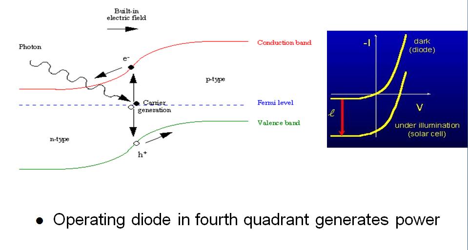
39 irradiated p/n-junction band pattern view (absorption p-zone) E = h depletion-zone U d P + P + P + P + P + - photocurrent - B - B - B - B - B - E F n type region E d + - Internal electrical field p type region Clemson Summer School Dr. Karl Molter / FH Trier / molter@fhtrier.de 39
40 p/n junction with irradiation crystal view h p-silizium diffusion n-silizium E electrical field depletion zone Clemson Summer School Dr. Karl Molter / FH Trier / molter@fhtrier.de 40
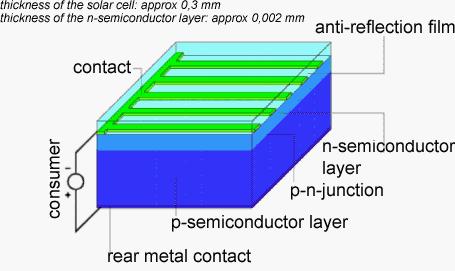
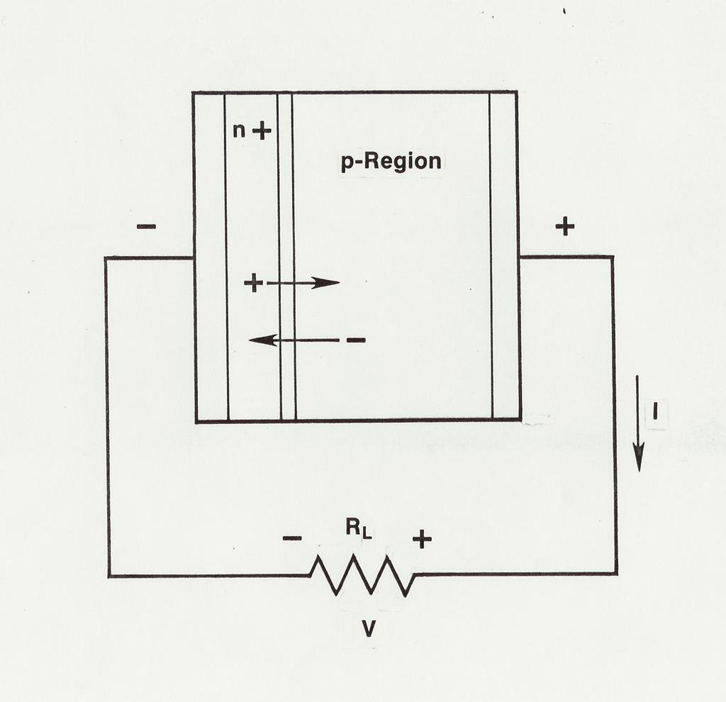
41 The real Silicon Solar-cell Front-contact Antireflectioncoating h - n-region p-region ~0,2µm ~300µm depletion zone Backside contact Clemson Summer School Dr. Karl Molter / FH Trier / molter@fhtrier.de 41
42
43
44
45 Clemson Summer School Dr. Karl Molter / FH Trier / molter@fhtrier.de 45
46
47
48
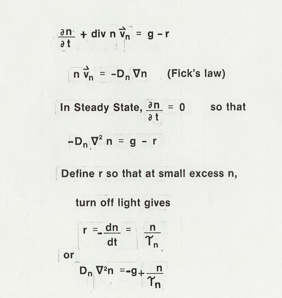
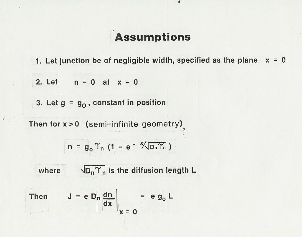
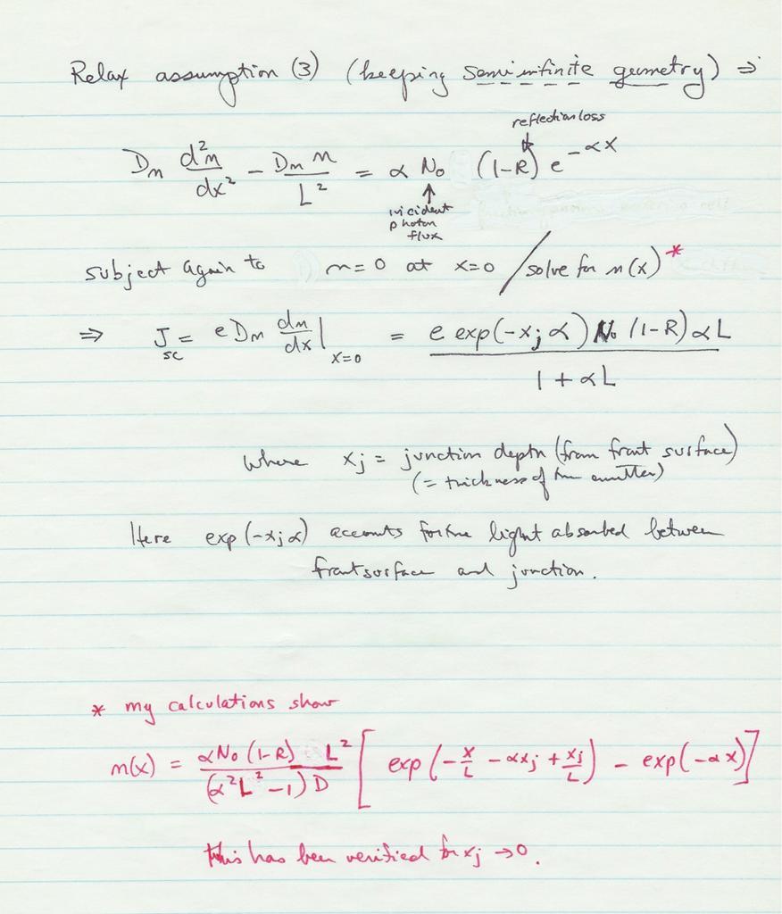
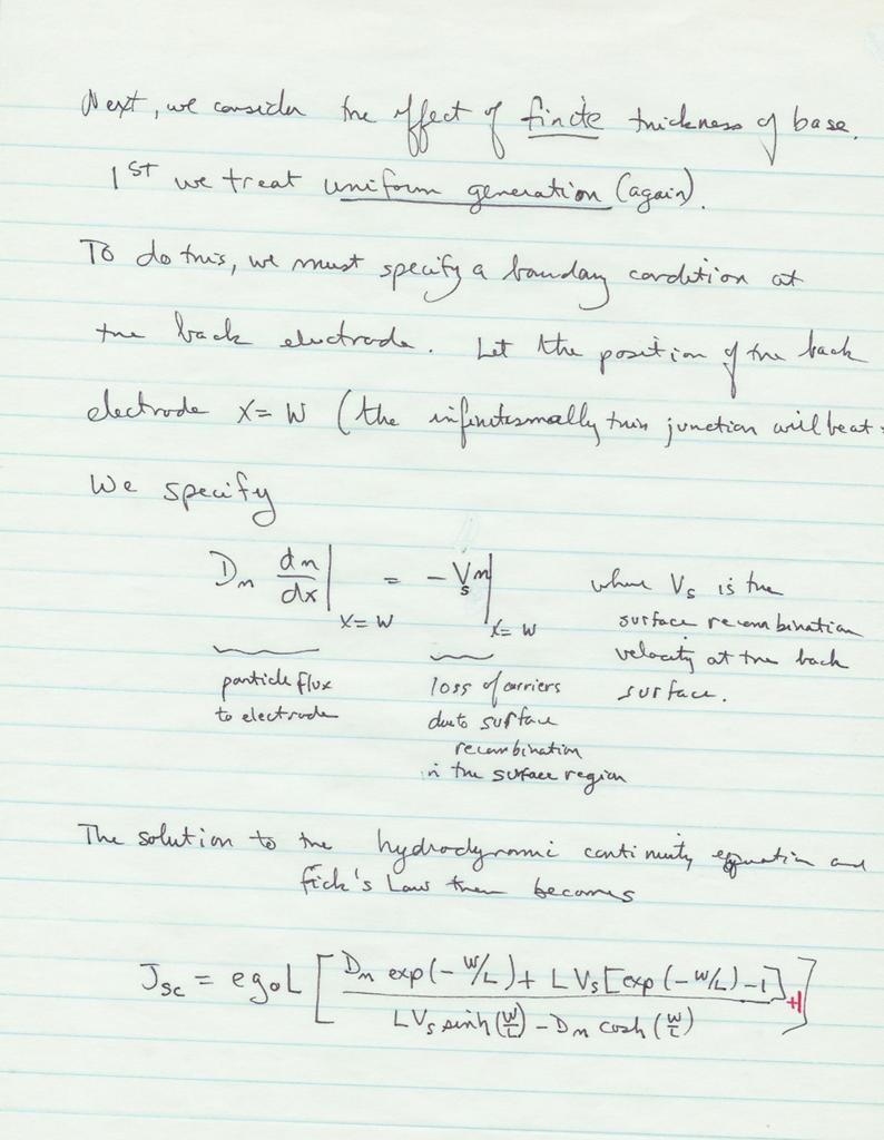
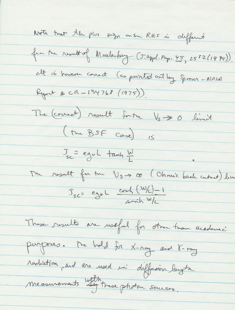
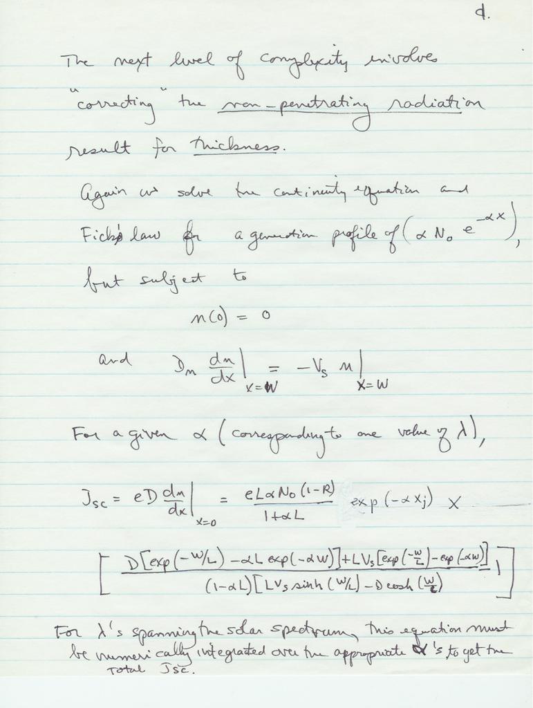
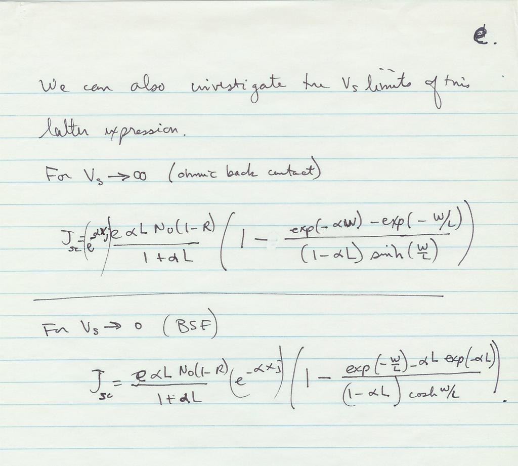
49
50
51
52
53
54
55
56
57 We now calculate the lightgenerated minority (diffusion) current
58
59 We now solve this differential equation under various boundary conditions: 1)uniform generation, semi-infinite geometry 2) generation decaying exponentially with position, semi-infinite geometry 3)uniform generation, finite thickness 4)generation decaying exponentially with position, finite thickness
60 n=0 x=0 x N P
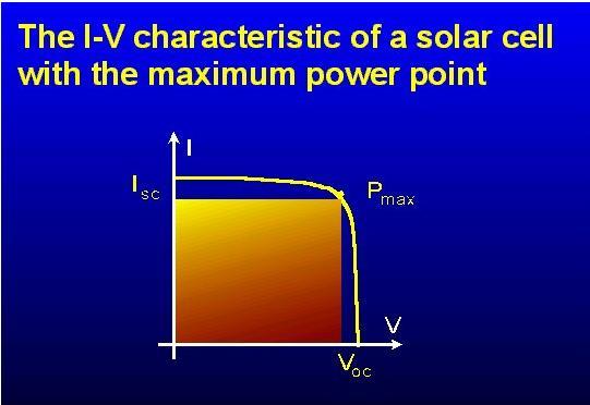
61
62
63
64
65
66
67
68
69 Heterojunctions
70
71 Efficiency Losses in Solar Cell 1 = Thermalization loss 2 and 3 = Junction and contact voltage loss 4 = Recombination loss
72
73
74
Lecture 1. OUTLINE Basic Semiconductor Physics. Reading: Chapter 2.1. Semiconductors Intrinsic (undoped) silicon Doping Carrier concentrations
 silicon Doping Carrier concentrations") Lecture 1 OUTLINE Basic Semiconductor Physics Semiconductors Intrinsic (undoped) silicon Doping Carrier concentrations Reading: Chapter 2.1 EE105 Fall 2007 Lecture 1, Slide 1 What is a Semiconductor? Low
Lecture 1 OUTLINE Basic Semiconductor Physics Semiconductors Intrinsic (undoped) silicon Doping Carrier concentrations Reading: Chapter 2.1 EE105 Fall 2007 Lecture 1, Slide 1 What is a Semiconductor? Low
Electrons are shared in covalent bonds between atoms of Si. A bound electron has the lowest energy state.
 Photovoltaics Basic Steps the generation of light-generated carriers; the collection of the light-generated carriers to generate a current; the generation of a large voltage across the solar cell; and
EE495/695 Introduction to Semiconductors I. Y. Baghzouz ECE Department UNLV
 EE495/695 Introduction to Semiconductors I Y. Baghzouz ECE Department UNLV Introduction Solar cells have always been aligned closely with other electronic devices. We will cover the basic aspects of semiconductor
3.1 Introduction to Semiconductors. Y. Baghzouz ECE Department UNLV
 3.1 Introduction to Semiconductors Y. Baghzouz ECE Department UNLV Introduction In this lecture, we will cover the basic aspects of semiconductor materials, and the physical mechanisms which are at the
PV Tutorial Allen Hermann, Ph. D. Professor of Physics Emeritus, and Professor of Music Adjunct, University of Colorado, Boulder, Colorado, USA and
 PV Tutorial Allen Hermann, Ph. D. Professor of Physics Emeritus, and Professor of Music Adjunct, University of Colorado, Boulder, Colorado, USA and Vice-president, NanoTech Inc. Lexington, Kentucky, USA
PN Junction
 P Junction 2017-05-04 Definition Power Electronics = semiconductor switches are used Analogue amplifier = high power loss 250 200 u x 150 100 u Udc i 50 0 0 50 100 150 200 250 300 350 400 i,u dc i,u u
The photovoltaic effect occurs in semiconductors where there are distinct valence and
 How a Photovoltaic Cell Works The photovoltaic effect occurs in semiconductors where there are distinct valence and conduction bands. (There are energies at which electrons can not exist within the solid)
Maria Carmela Di Piazza. Gianpaolo Vitale. Photovoltaic Sources. Modeling and Emulation. ^ Springer
 Maria Carmela Di Piazza Gianpaolo Vitale Photovoltaic Sources Modeling and Emulation ^ Springer Part I 1 From the Nuclear Fusion to the Radiated Energy on the Earth... 3 1.1 Inside the Universe 3 1.2 The
Basic Semiconductor Physics
 6 Basic Semiconductor Physics 6.1 Introduction With this chapter we start with the discussion of some important concepts from semiconductor physics, which are required to understand the operation of solar
EE 446/646 Photovoltaic Devices I. Y. Baghzouz
 EE 446/646 Photovoltaic Devices I Y. Baghzouz What is Photovoltaics? First used in about 1890, the word has two parts: photo, derived from the Greek word for light, volt, relating to electricity pioneer
PHOTOVOLTAICS Fundamentals
 PHOTOVOLTAICS Fundamentals PV FUNDAMENTALS Semiconductor basics pn junction Solar cell operation Design of silicon solar cell SEMICONDUCTOR BASICS Allowed energy bands Valence and conduction band Fermi
Electronics The basics of semiconductor physics
 Electronics The basics of semiconductor physics Prof. Márta Rencz, Gergely Nagy BME DED September 16, 2013 The basic properties of semiconductors Semiconductors conductance is between that of conductors
ET3034TUx Utilization of band gap energy
 ET3034TUx - 3.3.1 - Utilization of band gap energy In the last two weeks we have discussed the working principle of a solar cell and the external parameters that define the performance of a solar cell.
Electronic Circuits for Mechatronics ELCT 609 Lecture 2: PN Junctions (1)
") Electronic Circuits for Mechatronics ELCT 609 Lecture 2: PN Junctions (1) Assistant Professor Office: C3.315 E-mail: eman.azab@guc.edu.eg 1 Electronic (Semiconductor) Devices P-N Junctions (Diodes): Physical
Electronic Circuits for Mechatronics ELCT 609 Lecture 2: PN Junctions (1) Assistant Professor Office: C3.315 E-mail: eman.azab@guc.edu.eg 1 Electronic (Semiconductor) Devices P-N Junctions (Diodes): Physical
Photovoltaic cell and module physics and technology
 Photovoltaic cell and module physics and technology Vitezslav Benda, Prof Czech Technical University in Prague benda@fel.cvut.cz www.fel.cvut.cz 6/21/2012 1 Outlines Photovoltaic Effect Photovoltaic cell
LEC E T C U T R U E R E 17 -Photodetectors
 LECTURE 17 -Photodetectors Topics to be covered Photodetectors PIN photodiode Avalanche Photodiode Photodetectors Principle of the p-n junction Photodiode A generic photodiode. Photodetectors Principle
Lecture (02) Introduction to Electronics II, PN Junction and Diodes I
 Introduction to Electronics II, PN Junction and Diodes I") Lecture (02) Introduction to Electronics II, PN Junction and Diodes I By: Dr. Ahmed ElShafee ١ Agenda Current in semiconductors/conductors N type, P type semiconductors N Type Semiconductor P Type Semiconductor
Lecture (02) Introduction to Electronics II, PN Junction and Diodes I By: Dr. Ahmed ElShafee ١ Agenda Current in semiconductors/conductors N type, P type semiconductors N Type Semiconductor P Type Semiconductor
Chemistry Instrumental Analysis Lecture 8. Chem 4631
 Chemistry 4631 Instrumental Analysis Lecture 8 UV to IR Components of Optical Basic components of spectroscopic instruments: stable source of radiant energy transparent container to hold sample device
Qualitative Picture of the Ideal Diode. G.R. Tynan UC San Diego MAE 119 Lecture Notes
 Qualitative Picture of the Ideal Diode G.R. Tynan UC San Diego MAE 119 Lecture Notes Band Theory of Solids: From Single Attoms to Solid Crystals Isolated Li atom (conducting metal) Has well-defined, isolated
Photovoltaic cell and module physics and technology. Vitezslav Benda, Prof Czech Technical University in Prague
 Photovoltaic cell and module physics and technology Vitezslav Benda, Prof Czech Technical University in Prague benda@fel.cvut.cz www.fel.cvut.cz 1 Outlines Photovoltaic Effect Photovoltaic cell structure
electronics fundamentals
 electronics fundamentals circuits, devices, and applications THOMAS L. FLOYD DAVID M. BUCHLA Lesson 1: Diodes and Applications Semiconductors Figure 1-1 The Bohr model of an atom showing electrons in orbits
Chapter 7. Solar Cell
 Chapter 7 Solar Cell 7.0 Introduction Solar cells are useful for both space and terrestrial application. Solar cells furnish the long duration power supply for satellites. It converts sunlight directly
A SEMICONDUCTOR DIODE. P-N Junction
 A SEMICONDUCTOR DIODE P-N Junction Analog Electronics Pujianto Department of Physics Edu. State University of Yogyakarta A Semiconductor Devices A Semiconductor devices can be defined as a unit which consists,
ITT Technical Institute ET215 Devices I Unit 1
 ITT Technical Institute ET215 Devices I Unit 1 Chapter 1 Chapter 2, Sections 2.1-2.4 Chapter 1 Basic Concepts of Analog Circuits Recall ET115 & ET145 Ohms Law I = V/R If voltage across a resistor increases
Charge Carriers in Semiconductor
 Charge Carriers in Semiconductor To understand PN junction s IV characteristics, it is important to understand charge carriers behavior in solids, how to modify carrier densities, and different mechanisms
Introduction to Transistors. Semiconductors Diodes Transistors
 Introduction to Transistors Semiconductors Diodes Transistors 1 Semiconductors Typical semiconductors, like silicon and germanium, have four valence electrons which form atomic bonds with neighboring atoms
KATIHAL FİZİĞİ MNT-510
 KATIHAL FİZİĞİ MNT-510 YARIİLETKENLER Kaynaklar: Katıhal Fiziği, Prof. Dr. Mustafa Dikici, Seçkin Yayıncılık Katıhal Fiziği, Şakir Aydoğan, Nobel Yayıncılık, Physics for Computer Science Students: With
1 Name: Student number: DEPARTMENT OF PHYSICS AND PHYSICAL OCEANOGRAPHY MEMORIAL UNIVERSITY OF NEWFOUNDLAND. Fall :00-11:00
 1 Name: DEPARTMENT OF PHYSICS AND PHYSICAL OCEANOGRAPHY MEMORIAL UNIVERSITY OF NEWFOUNDLAND Final Exam Physics 3000 December 11, 2012 Fall 2012 9:00-11:00 INSTRUCTIONS: 1. Answer all seven (7) questions.
smal band gap Saturday, April 9, 2011
 small band gap upper (conduction) band empty small gap valence band filled 2s 2p 2s 2p hybrid (s+p)band 2p no gap 2s (depend on the crystallographic orientation) extrinsic semiconductor semi-metal electron
EE 5611 Introduction to Microelectronic Technologies Fall Tuesday, September 23, 2014 Lecture 07
 EE 5611 Introduction to Microelectronic Technologies Fall 2014 Tuesday, September 23, 2014 Lecture 07 1 Introduction to Solar Cells Topics to be covered: Solar cells and sun light Review on semiconductor
Electron Energy, E E = 0. Free electron. 3s Band 2p Band Overlapping energy bands. 3p 3s 2p 2s. 2s Band. Electrons. 1s ATOM SOLID.
 Electron Energy, E Free electron Vacuum level 3p 3s 2p 2s 2s Band 3s Band 2p Band Overlapping energy bands Electrons E = 0 1s ATOM 1s SOLID In a metal the various energy bands overlap to give a single
ESE370: Circuit-Level Modeling, Design, and Optimization for Digital Systems
 ESE370: Circuit-Level Modeling, Design, and Optimization for Digital Systems Lec 6: September 14, 2015 MOS Model You are Here: Transistor Edition! Previously: simple models (0 and 1 st order) " Comfortable
Chapter 1. Solar energy conversion: from amorphous silicon to Dye-Sensitized Solar Cells. 1.1 Photovoltaic history.
 Chapter 1 Solar energy conversion: from amorphous silicon to Dye-Sensitized Solar Cells 1.1 Photovoltaic history. 1.2 Operation of traditional photovoltaic devices. 1.3 Thin film solar cells. 1.4 Multijunction
Lecture (02) PN Junctions and Diodes
 PN Junctions and Diodes") Lecture (02) PN Junctions and Diodes By: Dr. Ahmed ElShafee ١ I Agenda N type, P type semiconductors N Type Semiconductor P Type Semiconductor PN junction Energy Diagrams of the PN Junction and Depletion
Lecture (02) PN Junctions and Diodes By: Dr. Ahmed ElShafee ١ I Agenda N type, P type semiconductors N Type Semiconductor P Type Semiconductor PN junction Energy Diagrams of the PN Junction and Depletion
Electro - Principles I
 Electro - Principles I Page 10-1 Atomic Theory It is necessary to know what goes on at the atomic level of a semiconductor so the characteristics of the semiconductor can be understood. In many cases a
e - Galvanic Cell 1. Voltage Sources 1.1 Polymer Electrolyte Membrane (PEM) Fuel Cell
 Fuel Cell") Galvanic cells convert different forms of energy (chemical fuel, sunlight, mechanical pressure, etc.) into electrical energy and heat. In this lecture, we are interested in some examples of galvanic cells.
Galvanic cells convert different forms of energy (chemical fuel, sunlight, mechanical pressure, etc.) into electrical energy and heat. In this lecture, we are interested in some examples of galvanic cells.
Lecture 2. Semiconductor Physics. Sunday 4/10/2015 Semiconductor Physics 1-1
 Lecture 2 Semiconductor Physics Sunday 4/10/2015 Semiconductor Physics 1-1 Outline Intrinsic bond model: electrons and holes Charge carrier generation and recombination Intrinsic semiconductor Doping:
Basic Physics of Semiconductors
 Basic Physics of Semiconductors Semiconductor materials and their properties PN-junction diodes Reverse Breakdown EEM 205 Electronics I Dicle University, EEE Dr. Mehmet Siraç ÖZERDEM Semiconductor Physics
Determination of properties in semiconductor materials by applying Matlab
 Determination of properties in semiconductor materials by applying Matlab Carlos Figueroa. 1, Raúl Riera A. 2 1 Departamento de Ingeniería Industrial. Universidad de Sonora A.P. 5-088, Hermosillo, Sonora.
February 1, 2011 The University of Toledo, Department of Physics and Astronomy SSARE, PVIC
 FUNDAMENTAL PROPERTIES OF SOLAR CELLS February 1, 2011 The University of Toledo, Department of Physics and Astronomy SSARE, PVIC Principles and Varieties of Solar Energy (PHYS 4400) and Fundamentals of
Lecture 12. Semiconductor Detectors - Photodetectors
 Lecture 12 Semiconductor Detectors - Photodetectors Principle of the pn junction photodiode Absorption coefficient and photodiode materials Properties of semiconductor detectors The pin photodiodes Avalanche
Ch/ChE 140a Problem Set #3 2007/2008 SHOW ALL OF YOUR WORK! (190 Points Total) Due Thursday, February 28 th, 2008
 Due Thursday, February 28 th, 2008") Ch/ChE 140a Problem Set #3 2007/2008 SHOW ALL OF YOUR WORK! (190 Points Total) Due Thursday, February 28 th, 2008 Please read chapter 6 (pp. 175-209) of Advanced Semiconductor Fundamentals by Pierret.
Ch/ChE 140a Problem Set #3 2007/2008 SHOW ALL OF YOUR WORK! (190 Points Total) Due Thursday, February 28 th, 2008 Please read chapter 6 (pp. 175-209) of Advanced Semiconductor Fundamentals by Pierret.
Session 6: Solid State Physics. Diode
 Session 6: Solid State Physics Diode 1 Outline A B C D E F G H I J 2 Definitions / Assumptions Homojunction: the junction is between two regions of the same material Heterojunction: the junction is between
Section 2: The Science of Solar Energy
 Section 2: The Science of Solar Energy SECTION 2: THE SCIENCE OF SOLAR ENERGY Solar Radiation 9 Solar radiation outside the earth s atmosphere is called extraterrestrial radiation. On average the extraterrestrial
Schottky Rectifiers Zheng Yang (ERF 3017,
 ECE442 Power Semiconductor Devices and Integrated Circuits Schottky Rectifiers Zheng Yang (ERF 3017, email: yangzhen@uic.edu) Power Schottky Rectifier Structure 2 Metal-Semiconductor Contact The work function
Semiconductor Physics. Lecture 3
 Semiconductor Physics Lecture 3 Intrinsic carrier density Intrinsic carrier density Law of mass action Valid also if we add an impurity which either donates extra electrons or holes the number of carriers
Semiconductor Physics fall 2012 problems
 Semiconductor Physics fall 2012 problems 1. An n-type sample of silicon has a uniform density N D = 10 16 atoms cm -3 of arsenic, and a p-type silicon sample has N A = 10 15 atoms cm -3 of boron. For each
High efficiency silicon and perovskite-silicon solar cells for electricity generation
 High efficiency silicon and perovskite-silicon solar cells for electricity generation Ali Dabirian Email: dabirian@ipm.ir 1 From Solar Energy to Electricity 2 Global accumulative PV installed In Iran it
Diodes. EE223 Digital & Analogue Electronics Derek Molloy 2012/2013.
 Diodes EE223 Digital & Analogue Electronics Derek Molloy 2012/2013 Derek.Molloy@dcu.ie Diodes: A Semiconductor? Conductors Such as copper, aluminium have a cloud of free electrons weak bound valence electrons
Charge Extraction. Lecture 9 10/06/2011 MIT Fundamentals of Photovoltaics 2.626/2.627 Fall 2011 Prof. Tonio Buonassisi
 Charge Extraction Lecture 9 10/06/2011 MIT Fundamentals of Photovoltaics 2.626/2.627 Fall 2011 Prof. Tonio Buonassisi 2.626/2.627 Roadmap You Are Here 2.626/2.627: Fundamentals Every photovoltaic device
FYS 3028/8028 Solar Energy and Energy Storage. Calculator with empty memory Language dictionaries
 Faculty of Science and Technology Exam in: FYS 3028/8028 Solar Energy and Energy Storage Date: 11.05.2016 Time: 9-13 Place: Åsgårdvegen 9 Approved aids: Type of sheets (sqares/lines): Number of pages incl.
Solar Cells Technology: An Engine for National Development
 IOSR Journal of Electrical and Electronics Engineering (IOSR-JEEE) e-issn: 2278-1676,p-ISSN: 2320-3331, Volume 7, Issue 5 (Sep. - Oct. 2013), PP 13-18 Solar Cells Technology: An Engine for National Development
Novel High-Efficiency Crystalline-Si-Based Compound. Heterojunction Solar Cells: HCT (Heterojunction with Compound. Thin-layer)
") Electronic Supplementary Material (ESI) for Physical Chemistry Chemical Physics. This journal is the Owner Societies 2014 Supplementary Information for Novel High-Efficiency Crystalline-Si-Based Compound
Electronic Supplementary Material (ESI) for Physical Chemistry Chemical Physics. This journal is the Owner Societies 2014 Supplementary Information for Novel High-Efficiency Crystalline-Si-Based Compound
Lecture 18. New gas detectors Solid state trackers
 Lecture 18 New gas detectors Solid state trackers Time projection Chamber Full 3-D track reconstruction x-y from wires and segmented cathode of MWPC z from drift time de/dx information (extra) Drift over
Materiales y tecnologías fotovoltaicas
 Materiales y tecnologías fotovoltaicas Amaru Palomino Töfflinger, Andrés Guerra, Rolf Grieseler, Roland Weingärtner Grupo de Ciencia de los Materiales Sección Física PUCP Materials Science Group Physics,
n N D n p = n i p N A
 Summary of electron and hole concentration in semiconductors Intrinsic semiconductor: E G n kt i = pi = N e 2 0 Donor-doped semiconductor: n N D where N D is the concentration of donor impurity Acceptor-doped
Temperature Dependent Current-voltage Characteristics of P- type Crystalline Silicon Solar Cells Fabricated Using Screenprinting
 Temperature Dependent Current-voltage Characteristics of P- type Crystalline Silicon Solar Cells Fabricated Using Screenprinting Process Hyun-Jin Song, Won-Ki Lee, Chel-Jong Choi* School of Semiconductor
Atoms? All matters on earth made of atoms (made up of elements or combination of elements).
.") Chapter 1 Atoms? All matters on earth made of atoms (made up of elements or combination of elements). Atomic Structure Atom is the smallest particle of an element that can exist in a stable or independent
Chapter 1 Atoms? All matters on earth made of atoms (made up of elements or combination of elements). Atomic Structure Atom is the smallest particle of an element that can exist in a stable or independent
5. Semiconductors and P-N junction
 5. Semiconductors and P-N junction Thomas Zimmer, University of Bordeaux, France Summary Learning Outcomes... 2 Physical background of semiconductors... 2 The silicon crystal... 2 The energy bands... 3
! Previously: simple models (0 and 1 st order) " Comfortable with basic functions and circuits. ! This week and next (4 lectures)
 Comfortable with basic functions and circuits. ! This week and next (4 lectures)") ESE370: CircuitLevel Modeling, Design, and Optimization for Digital Systems Lec 6: September 14, 2015 MOS Model You are Here: Transistor Edition! Previously: simple models (0 and 1 st order) " Comfortable
ESE370: CircuitLevel Modeling, Design, and Optimization for Digital Systems Lec 6: September 14, 2015 MOS Model You are Here: Transistor Edition! Previously: simple models (0 and 1 st order) " Comfortable
Lecture 3b. Bonding Model and Dopants. Reading: (Cont d) Notes and Anderson 2 sections
 Notes and Anderson 2 sections") Lecture 3b Bonding Model and Dopants Reading: (Cont d) Notes and Anderson 2 sections 2.3-2.7 The need for more control over carrier concentration Without help the total number of carriers (electrons and
Lecture 3b Bonding Model and Dopants Reading: (Cont d) Notes and Anderson 2 sections 2.3-2.7 The need for more control over carrier concentration Without help the total number of carriers (electrons and
Semiconductor Physics and Devices
 Syllabus Advanced Nano Materials Semiconductor Physics and Devices Textbook Donald A. Neamen (McGraw-Hill) Semiconductor Physics and Devices Seong Jun Kang Department of Advanced Materials Engineering
ESE370: Circuit-Level Modeling, Design, and Optimization for Digital Systems
 ESE370: Circuit-Level Modeling, Design, and Optimization for Digital Systems Lec 6: September 18, 2017 MOS Model You are Here: Transistor Edition! Previously: simple models (0 and 1 st order) " Comfortable
3.1 Absorption and Transparency
 3.1 Absorption and Transparency 3.1.1 Optical Devices (definitions) 3.1.2 Photon and Semiconductor Interactions 3.1.3 Photon Intensity 3.1.4 Absorption 3.1 Absorption and Transparency Objective 1: Recall
CLASS 12th. Semiconductors
 CLASS 12th Semiconductors 01. Distinction Between Metals, Insulators and Semi-Conductors Metals are good conductors of electricity, insulators do not conduct electricity, while the semiconductors have
Semiconductor Physics and Devices
 The pn Junction 1) Charge carriers crossing the junction. 3) Barrier potential Semiconductor Physics and Devices Chapter 8. The pn Junction Diode 2) Formation of positive and negative ions. 4) Formation
Mesoporous titanium dioxide electrolyte bulk heterojunction
 Mesoporous titanium dioxide electrolyte bulk heterojunction The term "bulk heterojunction" is used to describe a heterojunction composed of two different materials acting as electron- and a hole- transporters,
Ga and P Atoms to Covalent Solid GaP
 Ga and P Atoms to Covalent Solid GaP Band Gaps in Binary Group III-V Semiconductors Mixed Semiconductors Affect of replacing some of the As with P in GaAs Band Gap (ev) (nm) GaAs 1.35 919 (IR) GaP 2.24
Solar Photovoltaics under Partially Shaded Conditions. Vivek Agarwal Dept of Electrical Engineering
 Solar Photovoltaics under Partially Shaded Conditions Vivek Agarwal Dept of Electrical Engineering Neils Bohr s Atomic Model Increasing energy orbits n = 1 n = 2 n = 3 A photon is absorbed with energy,
Semiconductor Junctions
 8 Semiconductor Junctions Almost all solar cells contain junctions between different materials of different doping. Since these junctions are crucial to the operation of the solar cell, we will discuss
Review of Semiconductor Fundamentals
 ECE 541/ME 541 Microelectronic Fabrication Techniques Review of Semiconductor Fundamentals Zheng Yang (ERF 3017, email: yangzhen@uic.edu) Page 1 Semiconductor A semiconductor is an almost insulating material,
LECTURE 23. MOS transistor. 1 We need a smart switch, i.e., an electronically controlled switch. Lecture Digital Circuits, Logic
 LECTURE 23 Lecture 16-20 Digital Circuits, Logic 1 We need a smart switch, i.e., an electronically controlled switch 2 We need a gain element for example, to make comparators. The device of our dreams
A COMPARATIVE CHEMICAL STUDY OF THE TOP LAYERS OF TWO DIFFERENT QUALITY SILICON SOLAR CELLS
 A COMPARATIVE CHEMICAL STUDY OF THE TOP LAYERS OF TWO DIFFERENT QUALITY SILICON SOLAR CELLS M.J. Ariza and D.Leinen Departamento de Fisica Aplicada I, Facultad de Ciencias, Universidad de Málaga, E-2971
Chapter 2 The Well 9/5/2017. E E 480 Introduction to Analog and Digital VLSI Paul M. Furth New Mexico State University
 hapter 2 The Well E E 480 Introduction to Analog and Digital VLSI Paul M. Furth New Mexico State University p+ sub ~ 150 m thick, p-epi ~ 30 m thick All transistors go in p- epi layer Typical p- doping
Introduction to Semiconductor Physics. Prof.P. Ravindran, Department of Physics, Central University of Tamil Nadu, India
 Introduction to Semiconductor Physics 1 Prof.P. Ravindran, Department of Physics, Central University of Tamil Nadu, India http://folk.uio.no/ravi/cmp2013 Review of Semiconductor Physics Semiconductor fundamentals
Photovoltaic Energy Conversion. Frank Zimmermann
 Photovoltaic Energy Conversion Frank Zimmermann Solar Electricity Generation Consumes no fuel No pollution No greenhouse gases No moving parts, little or no maintenance Sunlight is plentiful & inexhaustible
Quiz #1 Practice Problem Set
 Name: Student Number: ELEC 3908 Physical Electronics Quiz #1 Practice Problem Set? Minutes January 22, 2016 - No aids except a non-programmable calculator - All questions must be answered - All questions
A semiconductor is an almost insulating material, in which by contamination (doping) positive or negative charge carriers can be introduced.
 positive or negative charge carriers can be introduced.") Semiconductor A semiconductor is an almost insulating material, in which by contamination (doping) positive or negative charge carriers can be introduced. Page 2 Semiconductor materials Page 3 Energy levels
Semiconductor A semiconductor is an almost insulating material, in which by contamination (doping) positive or negative charge carriers can be introduced. Page 2 Semiconductor materials Page 3 Energy levels
Avalanche breakdown. Impact ionization causes an avalanche of current. Occurs at low doping
 Avalanche breakdown Impact ionization causes an avalanche of current Occurs at low doping Zener tunneling Electrons tunnel from valence band to conduction band Occurs at high doping Tunneling wave decays
PHYSICAL ELECTRONICS(ECE3540) CHAPTER 9 METAL SEMICONDUCTOR AND SEMICONDUCTOR HETERO-JUNCTIONS
 CHAPTER 9 METAL SEMICONDUCTOR AND SEMICONDUCTOR HETERO-JUNCTIONS") PHYSICAL ELECTRONICS(ECE3540) CHAPTER 9 METAL SEMICONDUCTOR AND SEMICONDUCTOR HETERO-JUNCTIONS Tennessee Technological University Monday, November 11, 013 1 Introduction Chapter 4: we considered the semiconductor
PHYSICAL ELECTRONICS(ECE3540) CHAPTER 9 METAL SEMICONDUCTOR AND SEMICONDUCTOR HETERO-JUNCTIONS Tennessee Technological University Monday, November 11, 013 1 Introduction Chapter 4: we considered the semiconductor
Basic cell design. Si cell
 Basic cell design Si cell 1 Concepts needed to describe photovoltaic device 1. energy bands in semiconductors: from bonds to bands 2. free carriers: holes and electrons, doping 3. electron and hole current:
Semiconductor physics I. The Crystal Structure of Solids
 Lecture 3 Semiconductor physics I The Crystal Structure of Solids 1 Semiconductor materials Types of solids Space lattices Atomic Bonding Imperfection and doping in SOLIDS 2 Semiconductor Semiconductors
Semiconductor Detectors
 Semiconductor Detectors Summary of Last Lecture Band structure in Solids: Conduction band Conduction band thermal conductivity: E g > 5 ev Valence band Insulator Charge carrier in conductor: e - Charge
Technology Options for Photo voltaic Solar Cells. Claudio Fiegna
 Technology Options for Photo voltaic Solar Cells Claudio Fiegna Outline Introduction Working principle for solar cells Silicon based solar cells Crystalline Thin film a Si or c Si Other thin film technologies
Photosynthesis & Solar Power Harvesting
 Lecture 23 Semiconductor Detectors - Photodetectors Principle of the pn junction photodiode Absorption coefficient and photodiode materials Properties of semiconductor detectors The pin photodiodes Avalanche
Silicon Detectors in High Energy Physics
 Thomas Bergauer (HEPHY Vienna) IPM Teheran 22 May 2011 Sunday: Schedule Silicon Detectors in Semiconductor Basics (45 ) Detector concepts: Pixels and Strips (45 ) Coffee Break Strip Detector Performance
OPTI510R: Photonics. Khanh Kieu College of Optical Sciences, University of Arizona Meinel building R.626
 OPTI510R: Photonics Khanh Kieu College of Optical Sciences, University of Arizona kkieu@optics.arizona.edu Meinel building R.626 Announcements Homework #6 is assigned, due May 1 st Final exam May 8, 10:30-12:30pm
PHYSICAL ELECTRONICS(ECE3540) CHAPTER 9 METAL SEMICONDUCTOR AND SEMICONDUCTOR HETERO-JUNCTIONS
 CHAPTER 9 METAL SEMICONDUCTOR AND SEMICONDUCTOR HETERO-JUNCTIONS") PHYSICAL ELECTRONICS(ECE3540) CHAPTER 9 METAL SEMICONDUCTOR AND SEMICONDUCTOR HETERO-JUNCTIONS Tennessee Technological University Wednesday, October 30, 013 1 Introduction Chapter 4: we considered the
PHYSICAL ELECTRONICS(ECE3540) CHAPTER 9 METAL SEMICONDUCTOR AND SEMICONDUCTOR HETERO-JUNCTIONS Tennessee Technological University Wednesday, October 30, 013 1 Introduction Chapter 4: we considered the
First-Hand Investigation: Modeling of Semiconductors
 perform an investigation to model the behaviour of semiconductors, including the creation of a hole or positive charge on the atom that has lost the electron and the movement of electrons and holes in
Misan University College of Engineering Electrical Engineering Department. Exam: Final semester Date: 17/6/2017
 Misan University College of Engineering Electrical Engineering Department Subject: Electronic I Class: 1 st stage Exam: Final semester Date: 17/6/2017 Examiner: Dr. Baqer. O. TH. Time: 3 hr. Note: Answer
Research Article Modeling and Optimization of Advanced Single- and Multijunction Solar Cells Based on Thin-Film a-si:h/sige Heterostructure
 International Scholarly Research Network ISRN Renewable Energy Volume 211, Article ID 712872, 8 pages doi:1.542/211/712872 Research Article Modeling and Optimization of Advanced Single- and Multijunction
Energy sources. 4. Solar Energy I
 4. Solar Energy I All the energy strategies include solar energy as a major option for middle term and long term development. Although the solar energy is considered unconventional yet, owing to some advantages
Junction Diodes. Tim Sumner, Imperial College, Rm: 1009, x /18/2006
 Junction Diodes Most elementary solid state junction electronic devices. They conduct in one direction (almost correct). Useful when one converts from AC to DC (rectifier). But today diodes have a wide
Solar Photovoltaics & Energy Systems
 Solar Photovoltaics & Energy Systems Lecture 4. Crystalline Semiconductor Based Solar Cells ChE-600 Wolfgang Tress, May 2016 1 Photovoltaic Solar Energy Conversion 2 Semiconductor vs. Heat Engine spectral
ECE 442. Spring, Lecture -2
 ECE 442 Power Semiconductor Devices and Integrated circuits Spring, 2006 University of Illinois at Chicago Lecture -2 Semiconductor physics band structures and charge carriers 1. What are the types of
3. PHOTOVOLTAIC CONVERSION
 3. PHOTOVOLTAIC CONVERSION Content 3.1 Solar radiation 3.2 Photoelectric conversion of solar radiation 3.3 The photoelectric effect in the homo-junction p-n. 3.4 Solar cell parameters 3.5 Energy losses
ECE 335: Electronic Engineering Lecture 2: Semiconductors
 Faculty of Engineering ECE 335: Electronic Engineering Lecture 2: Semiconductors Agenda Intrinsic Semiconductors Extrinsic Semiconductors N-type P-type Carrier Transport Drift Diffusion Semiconductors
Electronics EC /2/2012. * In-class exams: 40% 7 th week exam 25% 12 th week exam 15%
 Arab Academy for Science, Technology and Maritime Transport Electronics EC 331 Dr. Mohamed Hassan Course Assessment * In-class exams: 40% 7 th week exam 25% 12 th week exam 15% *Tutorial exams and activities:
Energetic particles and their detection in situ (particle detectors) Part II. George Gloeckler
 Part II. George Gloeckler") Energetic particles and their detection in situ (particle detectors) Part II George Gloeckler University of Michigan, Ann Arbor, MI University of Maryland, College Park, MD Simple particle detectors Gas-filled
Energetic particles and their detection in situ (particle detectors) Part II George Gloeckler University of Michigan, Ann Arbor, MI University of Maryland, College Park, MD Simple particle detectors Gas-filled
an introduction to Semiconductor Devices
 an introduction to Semiconductor Devices Donald A. Neamen Chapter 6 Fundamentals of the Metal-Oxide-Semiconductor Field-Effect Transistor Introduction: Chapter 6 1. MOSFET Structure 2. MOS Capacitor -