Mixed Signal IC Design Notes set 4: Broadband Design Techniques
|
|
|
- Erick Richardson
- 6 years ago
- Views:
Transcription
1 Mixed Sal C Des Notes set 4: Broadband Des Techniques Mark odwell University of California, Santa Barbara rodwell@ece.ucsb.edu , fax
2 Gett ore bandwidth At this pot we have learned basics (MOTC etc) How can we et ore bandwidth.? esistive feedback transconductance-transipedance eitter-follower buffers, nefits and headaches eitter deeneration basics eitter deeneration and area scal ft-doubler staes.. distributed aplifiers broadband / peak with LC networks. exaples.
3 Eitter Deeneration, e Ce e Ce e Eitter deeneration was troduced us only an eitter resistance. We will fd we stead want an C cobation such that C e e C /.
4 Eitter Deeneration, 2 - C Ce e Ce e Next note that the topoloy is such that we can work with bb, C cb etc reoved, and add the back later...
5 Eitter Deeneration, 3 1 b C 2-3 e Work fro : 1 But So, and ( 1/ jωc ) (note that the frequency dependent ters cancel) Z bb jωc 2 E C 3 jωc cb /( E E 2 1/ jωc E (1 1 so ) and E ) 3 1 ( * ) etc can now added back...they dont chane E jωc Ce e
6 Eitter Deeneration, Suary Ccbx Ccbx bb Ccbi bb Ccbi C - - Ce e (1 1 C C E 1, extrsic (1 E ) ) Other eleent values do not chane...
7 Eitter Deeneration, Unbypassed eitter resistance ex C - C ex - 1, extrsic (1 E ) can shown by eleentary nodal analysis, work throuh Key observation: deeneration by this ethod results a series put resistance, which can crease C char tie.
8 Eitter Deeneration, cobation case Ccbx bb Ccbi bb Ccbx Ccbi C ex C ext - - Ce ex e C (1 C E ) 1 1, extrsic (1 E )
9 Eitter Deeneration and Area Scal 1 Consider the CS stae. f then we have a 1 C ( en bb ) C cb eitter area Ae current density Je Current Ae*Jee transconductance put capacitancec collector capacitanceccb base resistancebb we desire a [( )(1 ) ] en bb a A, ext L, ext L L,
10 Eitter Deeneration and Area Scal 2 eitter area Ae current density Je Current Ae*Jee transconductance put capacitancec collector capacitanceccb base resistancebb Ce e Bier transistor, fore deeneration eitter area kae current density Je Current kae*jeke transconductancek put capacitancekc collector capacitancekccb base resistancebb/k now deenerate: e picked such that (1e)k trsic transconductancek extrsic transconductancek/(1e) put capacitancekc/(1e)c collector capacitancekccb base resistancebb/k
11 Eitter Deeneration and Area Scal 3 Ce e We have ade the transistor K ties bier, then deenerated by K :1. We are left with the orial and C, but have creased Ccb by K :1and decreased K :1 a a 1 1 C en C en k C cb bb So, appropriate choice of Cbb [ (1 )] kc [ (1 ) ], ext Ccb, and ives the hihest bandwidth bb kc cb en L k bb (1, ext cb bb by ), ext k k exchanes delay ters associated with bb vs L en L L L
12 Eitter Deeneration and Area Scal 4: Eitter Follower Case Why iht we want to do this?
13 Eitter Deeneration and Area Scal 5: Eitter Follower Case Ccb1 1 Ccb2 L bb1 C1 bb2 C2 Consider only ters a1associated with the CE stae, bb2 a1... kccb2 out,1 k Note that the undeenerated ( 1 ) bb C bb2 L L C2 k tieconstant of an HBT, ext is several ties1/ 2πf τ, and can a ajor bandwidth liit. Area scal/deeneration as above is one ethod to address this. out,1
14 Ft-doubler staes.the Darlton evisited 1 L 1 L Q1 Q2 ee ee C1 C2 1 L bb1 bb2 ee C1 C2 ecall the iproveent Dap provided by ee. is there a larer lesson here?
15 2 Kds of Darlton: en L en L Q1 Q2 Q1 Q2 ee ee EF collector rounded Collectors tied toether f collectors are tied toether: AC collector currents of both transistors contribute to output :) Both transistor Ccb's undero Miller ultiplication :(
16 Ft-doubler staes 2 c1 out 1 - C1 e1 11 c2 ee1/ C2
17 Ft-doubler staes 3 out ee ee ee ee ee ee ee ee e e c C j C j C C C j C j C j C j C j ω ω ω ω ω ω ω / 2 / hence and 2 / 2 /...so ) ( 1/...hence / such that Choose ) (1 ) / (1 ) /(1 ) / (1,, : Work fro out ee1/1 C2 C c1 c2 e1 out
18 Ft-doubler staes 4 c1 out 1 C1 - ee1/1 e c C/2 C2 out / jωc / 2 and out 2 / jωc..we have doubled f τ! 2 f τ / jf Note that this analysis has ored bb and Ccb...we have certaly not doubled fax, nor will we have doubled overall circuit bandwidth, iven the presence of these other parasitics.
19 ft-doubler vs Darlton thk ters of current as: H21 (2*H21H21*H21) (1H21) H21(1H21) C2 Current a is Sce / out Y c1 2H out c2 21 / ( H / jf ) Current a varies at lower frequencies as ( 2H 21 1 ) 2 21 ( H 2( f where / jf / jf which ives hih current a but neative put conductance 21 2 τ ) 2 ( ( 1 f f τ τ H 21 2 ) ) 2 2 f τ )... / jf
20 ft-doubler vs Darlton thk ters of current as: H21 2*H21 (1H21) H21 C2 H21 Current a is Sce / out Y c1 2H out c2 21 / 2H 1 2( f / 21 where H jf ) 2 jf 2 f Current a varies at all frequencies as (2 f τ τ 21 ( jf τ f τ 1 / jf (2πC / jf ) 2 ) / 2)
21 ft-doubler vs Darlton current as:
22 ft-doubler correction for Base resistance LCbb/ c1 out 1 - C1 e1 11 c2 ee1/1 LCbb/ bb 2 22 C2 The dicated ductance is necessary for equal current splitt tween the 2 transistors the presence of bb. n this case the put ipedance is C/2 series with bb/2 aa note that this correction is sificant cause bbc>>c/
23 ft-doubler vs Darlton What is the conclusion of all this? We can view the ft-doubler as a special case of the connected-collector Darlton with heavy eitter-follower load: this case the second-order (resonant) response is entirely suppressed. More enerally we iht vary the EF load to vary the dap. (The particular case of power aplifiers favors the ft-doubler due to efficiency reasons )
24 Tun: to prevent reflections, to peak a Zo Zo C Zo outzo S 21 1 Zo / 2 jωcz / 2 jωcz / S11, where Z 1 0 / 2 Zo jωcz jωc The put capacitance has hurt both S11and S21, put atch and a 0
25 Pi-section put tun. Zo L Zo CxC/2 Zo CC/2 outzo Absorb the transistor put capacitance to a pi -section C C L τz Effective for freqeucies such that the pi - section isshort (hence o C / 2 τ / Z (2C Z o ) Z f0 < 1/ πzoc) o o 2 Ga flatness and atch iproved for f<fo, but ade worse for f>f0
26 T-section put tun. Zo L/2 Zo Zo L/2 CC outzo Absorb the transistor put capacitance to a T -section C C L τz o C τ / Z (2C Z o ) Z o o Effective for freqeucies such that the pi - section isshort (hence f0 < 1/ πzoc) Note that for a iven C, we have doubled fo relative to the pi -section case...
27 T-section tun feedback aplifiers Zo L/2 Zo f L/2 CC Zo L/2 Lf Zo Zo outzo CC By Miller Approxiation : L f f Z o (1 A) ( L / 2)(1 A) This is frequently used 50 Oh FBAs...daner is reduced stability.
28 Brided-T-section put tun. Zo L/2 Zo C/2 Zo L/2 CC outzo C C L τz o C τ / Z (2C Z o ) Z o o nsofar as the transistor has an put ipedance odeled by C, S11is exactly zero.s21 nevertheless rolls off at about the sae frequency as the T -section case...

29 Brided-T-section put tun. Karthik Krishnaurthi
30 Tun Networks use Microstrip eleents... Zo L CxC/2 Zo CC/2 Zo L CxC/2 Zo CC/2 Zo L Cx CC/2 Zo
31 Distributed Aplifiers : Theory synthetic dra le synthetic ate le HEMT put/output capacitances absord to artificial put/output les broadband circuit ; a/bandwidth liited by HEMT resistive parasitics (f ax ) distributed structure Bra frequency put/output transission le sk-effect losses
32 Synthetic Transission Les transission le section le section ductance le section capacitance HEMT put capacitance synthetic put/output le fored by transission le sections transission le characteristic ipedance Z L/C cutoff (Bra) frequency f B 1/ π LC delay T LC
33 Transission Le Loss lossless le frequency-dependent loss α π f C1 Z0 / 2 frequency-dependent loss α Z0 / 2
34 HEMT Equivalent Circuit siplified equivalent circuit eleent values scale with HEMT size fτ 2πC s f f r ds / 4r / ax τ i
35 CS HEMT TWA
36 CS HEMT TWA--LC equivalent
37 CS HEMT TWA--SS odel
38 TWA liits to a and bandwidth... Gate (put)le loss : 2 Nα < 1/ 2...sets a hih frequency liit causeα ω C Dra (output) Le Loss Nα nput - Output Delay Misatch Low - Frequency Ga S 21 N(T d ate < 1/ 2...sets a a liit causeα T N dra ( Z o ) < just requires / 2 we et des riht... / 2)(capacitive deeneration ratio)...toether with above liits, sets feasible a - bandwidth Bra Frequency f < 1/ π LC...can ade very hih with lots of very sall transistors...no proble... d Z o ds 2 i...

39 Undaped Darlton FBA S S S
40 Feedback Aplifier with Follower Driv ft-doubler 10 Gas, db S 21 S S Frequency, GHz

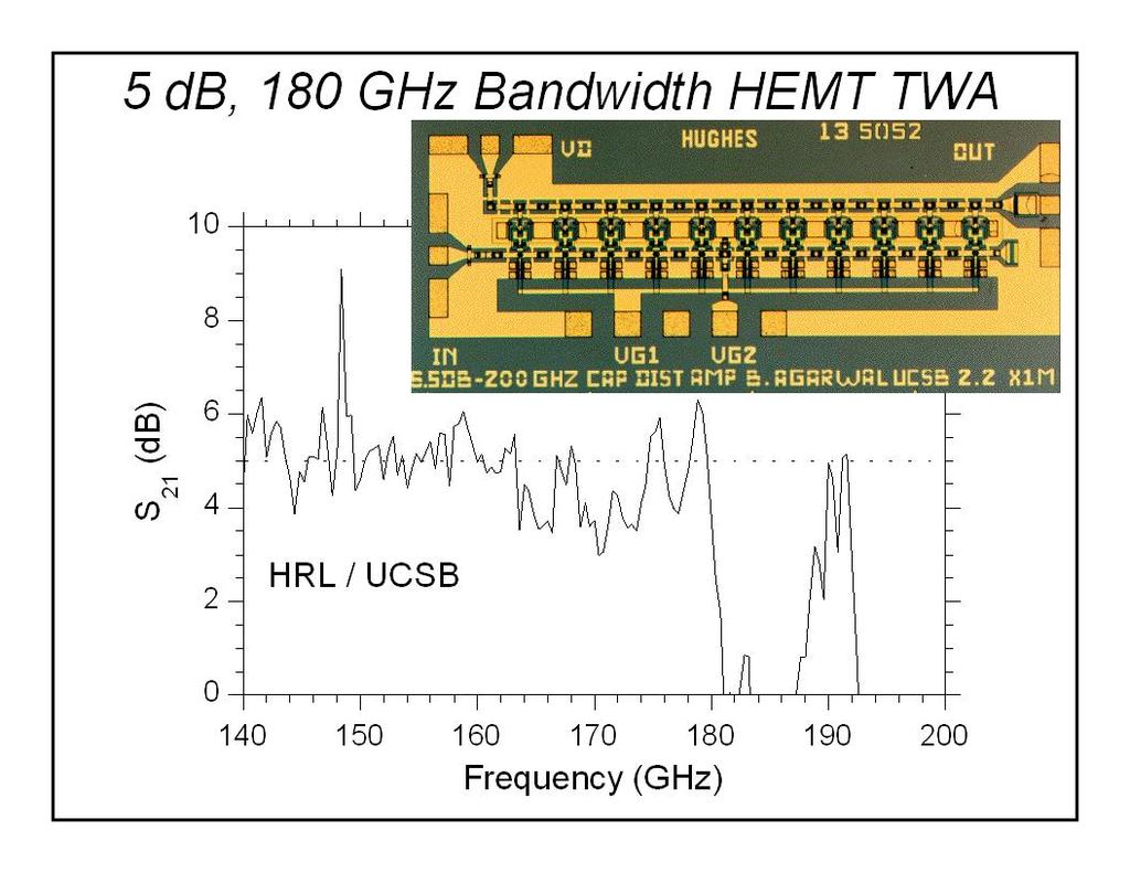
41 80 GHz HBT Distributed Aplifier S 21 5 Gas, db S S Frequency, GHz
42 dfdfasddffasdfd
ECEN326: Electronic Circuits Fall 2017
 EEN36: Electronic ircuits Fall 07 ecture 5: Frequency esponse a Palero Analo & Mixed-al enter Texas A&M University Announceents HW5 due / Exa /6 9:0-0:0 (0 extra utes) losed book w/ one standard note sheet
Chapter 11 Frequency Response. EE105 - Spring 2007 Microelectronic Devices and Circuits. High Frequency Roll-off of Amplifier. Gain Roll-off Thru C L
 EE05 - Spr 2007 Microelectronic Devices and ircuits ecture 9 Frequency Response hapter Frequency Response. General onsiderations.2 Hih-Frequency Models of Transistors.3 Frequency Response of S Staes.4
Lecture 21. REMINDERS Review session: Fri.11/9,3 5PMin306Soda in 306 (HP Auditorium) Midterm #2 (Thursday 11/15, 3:30 5PM in Sibley Auditorium)
 Midterm #2 (Thursday 11/15, 3:30 5PM in Sibley Auditorium)") Lecture EMINES eiew session: Fri./9,3 5PM306Soda 306 (HP Auditoriu) Midter # (Thursday /5, 3:30 5PM Sibley Auditoriu) OUTLINE Frequency esponse eiew of basic concepts hih frequency MOSFET odel S stae G
Lecture EMINES eiew session: Fri./9,3 5PM306Soda 306 (HP Auditoriu) Midter # (Thursday /5, 3:30 5PM Sibley Auditoriu) OUTLINE Frequency esponse eiew of basic concepts hih frequency MOSFET odel S stae G
ECEN326: Electronic Circuits Fall 2017
 ECEN36: Electronic Circuits Fall 07 Lecture 7: Feedback Sa Palero Analo & Mixed-Sal Center Texas A&M University Announceents Hoework 7 due /9 Exa 3 / 8:00-0:00 Closed book w/ one standard note sheet 8.5
Lab 4: Frequency Response of CG and CD Amplifiers.
 ESE 34 Electronics aboratory B Departent of Electrical and Coputer Enineerin Fall 2 ab 4: Frequency esponse of CG and CD Aplifiers.. OBJECTIVES Understand the role of input and output ipedance in deterinin
Chapter 2. Small-Signal Model Parameter Extraction Method
 Chapter Sall-Signal Model Paraeter Extraction Method In this chapter, we introduce a new paraeter extraction technique for sall-signal HBT odeling. Figure - shows the sall-signal equivalent circuit of
Mixed-Signal IC Design Notes set 1: Quick Summary of Device Models
 ECE194J /594J notes, M. Rodwell, copyrihted 2011 Mixed-Sinal IC Desin Notes set 1: Quick Summary of Device Models Mark Rodwell University of California, Santa Barbara rodwell@ece.ucsb.edu 805-893-3244,
Lecture 10 OUTLINE. Reading: Chapter EE105 Spring 2008 Lecture 10, Slide 1 Prof. Wu, UC Berkeley
 Lecture 0 OUTLIN BJT Aplifiers (3) itter follower (Coon-collector aplifier) Analysis of eitter follower core Ipact of source resistance Ipact of arly effect itter follower with biasin eadin: Chapter 5.3.3-5.4
HY:433 Σχεδίαση Αναλογικών/Μεικτών και Υψισυχνών Κυκλωμάτων
 HY:433 Σχεδίαση Αναλογικών/Μεικτών και Υψισυχνών Κυκλωμάτων «Low Noie Aplifier» Φώτης Πλέσσας fplea@e-ce.uth.r F eceiver Antenna BPF LNA BPF Mixer BPF3 IF Ap Deodulator F front end LO LNA De Conideration
Example: High-frequency response of a follower
 Example: Hih-requency response o a ollower o When body eects are cluded, db actually appears between dra and round. ce both termals o db are rounded, it does not aect the circuit. o d is also between the
ECEG 351 Electronics II Spring 2017
 G 351 lectronics Sprin 2017 Review Topics for xa #1 Please review the xa Policies section of the xas pae at the course web site. Please especially note the followin: 1. You will be allowed to use a non-wireless
EE5900 Spring Lecture 4 IC interconnect modeling methods Zhuo Feng
 EE59 Spring Parallel LSI AD Algoriths Lecture I interconnect odeling ethods Zhuo Feng. Z. Feng MTU EE59 So far we ve considered only tie doain analyses We ll soon see that it is soeties preferable to odel
ECEG 351 Electronics II Spring 2017
 ECEG 351 Electronics Sprin 017 Review Topics for Exa #3 Please review the Exa Policies section of the Exas pae at the course web site. You should especially note the followin: 1. You will be allowed to
Chapter 5 Impedance Matching and Tuning
 3/25/29 section 5_1 Match with umped Elements 1/3 Chapter 5 Impedance Match and Tun One of the most important and fundamental two-port networks that microwave eneers des is a lossless match network (otherwise
Lecture 36: MOSFET Common Drain (Source Follower) Amplifier.
 Amplifier.") Whites, EE 320 Lecture 36 Pae 1 of 10 Lecture 36: MOSFET Coon Drain (Source Follower) Aplifier. The third, and last, discrete-for MOSFET aplifier we ll consider in this course is the coon drain aplifier.
Whites, EE 320 Lecture 36 Pae 1 of 10 Lecture 36: MOSFET Coon Drain (Source Follower) Aplifier. The third, and last, discrete-for MOSFET aplifier we ll consider in this course is the coon drain aplifier.
Chapter 28: Alternating Current
 hapter 8: Alternating urrent Phasors and Alternating urrents Alternating current (A current) urrent which varies sinusoidally in tie is called alternating current (A) as opposed to direct current (D).
ECE 145A / 218 C, notes set 3: Two-Port Parameters
 class notes, M. odwell, copyrihted 9-4 ECE 45A / 8 C, notes set 3: Two-Port Parameters Mark odwell University of California, anta Barbara rodwell@ece.ucsb.edu 85-893-344, 85-893-36 fax Device Descriptions
Lecture #26. Small Signal Model
 ecture #6 ANNOUNCEMEN he lowest H grade will be dropped for each student OUNE Sall-signal MOSFE odel MOSFE scaling elocity uration Short-channel MOSFEs EE30 ecture 6, Slide Sall Signal Model Conductance
Introduction to CMOS RF Integrated Circuits Design
 Introduction to CMO F Interated Circuit Dein III. Low Noie Aplifier Introduction to CMO F Interated Circuit Dein Fall 0, Prof. JianJun Zhou III- Outline Fiure of erit Baic tructure Input and output atchin
Assignment 3 ELEC 312/Winter 12 R.Raut, Ph.D.
 Page 1 of 3 ELEC 312: ELECTRONICS II : ASSIGNMENT-3 Department of Electrical and Computer Engineering Winter 2012 1. A common-emitter amplifier that can be represented by the following equivalent circuit,
Switching circuits: basics and switching speed
 ECE137B notes; copyright 2018 Switching circuits: basics and switching speed Mark Rodwell, University of California, Santa Barbara Amplifiers vs. switching circuits Some transistor circuit might have V
EE 330 Lecture 30. Basic amplifier architectures
 33 Lecture 3 asic aplifier architectures asic plifier Structures MOS and ipolar Transistors oth have 3 priary terinals MOS transistor has a fourth terinal that is generally considered a parasitic D terinal
Introduction: the common and the differential mode components of two voltages. differential mode component: v d = v 1 - v 2 common mode component:
 EECTONCS-1 CHPTE 3 DFFEENT MPFES ntroduction: the common and the differential mode components of two voltaes v d v c differential mode component: v d = v 1 - v common mode component: v1 v v c = v 1 v vd
High Speed Mixed Signal IC Design notes set 8. Noise in Electrical Circuits: circuit noise analysis
 C145C /18C otes, M. odwell, copyrihted 007 Hih peed Mixed ial C Desi otes set 8 Noise i lectrical Circuits: circuit oise aalysis Mark odwell Uiversity of Califoria, ata Barbara rodwell@ece.ucsb.edu 805-893-344,
EE 330 Lecture 31. Basic amplifier architectures. Common Emitter/Source Common Collector/Drain Common Base/Gate
 33 Lecture 3 asic aplifier architectures oon itter/source oon ollector/drain oon ase/gate eview fro arlier Lecture Two-port representation of aplifiers plifiers can be odeled as a two-port y 2 2 y y 22
Electronic Circuits Summary
 Electronic Circuits Summary Andreas Biri, D-ITET 6.06.4 Constants (@300K) ε 0 = 8.854 0 F m m 0 = 9. 0 3 kg k =.38 0 3 J K = 8.67 0 5 ev/k kt q = 0.059 V, q kt = 38.6, kt = 5.9 mev V Small Signal Equivalent
EE 330 Lecture 33. Basic amplifier architectures Common Emitter/Source Common Collector/Drain Common Base/Gate. Basic Amplifiers
 33 Lecture 33 asic aplifier architectures oon itter/source oon ollector/drain oon ase/gate asic plifiers nalysis, Operation, and Desin xa 3 Friday pril 3 eview Previous Lecture Two-Port quivalents of Interconnected
Chapter 10 ACSS Power
 Objectives: Power concepts: instantaneous power, average power, reactive power, coplex power, power factor Relationships aong power concepts the power triangle Balancing power in AC circuits Condition
Lecture 28: Single Stage Frequency response. Context
 Lecure 28: Single Sage Frequency response Prof J. S. Sih Conex In oday s lecure, we will coninue o look a he frequency response of single sage aplifiers, saring wih a ore coplee discussion of he CS aplifier,
Circuit Topologies & Analysis Techniques in HF ICs
 Circuit Topologies & Analysis Techniques in HF ICs 1 Outline Analog vs. Microwave Circuit Design Impedance matching Tuned circuit topologies Techniques to maximize bandwidth Challenges in differential
EE 434 Lecture 16. Small signal model Small signal applications in amplifier analysis and design
 EE 434 Lecture 16 Sall sinal odel Sall sinal applications in aplifier analysis and desin Quiz 13 The of an n-channel OS transistor that has a quiescent current of 5A was easured to be 10A/. If the lenth
Lecture 23 Frequency Response of Amplifiers (I) Common Source Amplifier. December 1, 2005
 Common Source Amplifier. December 1, 2005") 6.02 Microelectronic Devices and Circuits Fall 2005 Lecture 23 Lecture 23 Frequency Response of Amplifiers (I) Common Source Amplifier December, 2005 Contents:. Introduction 2. Intrinsic frequency response
6.02 Microelectronic Devices and Circuits Fall 2005 Lecture 23 Lecture 23 Frequency Response of Amplifiers (I) Common Source Amplifier December, 2005 Contents:. Introduction 2. Intrinsic frequency response
Lecture 37: Frequency response. Context
 EECS 05 Spring 004, Lecture 37 Lecture 37: Frequency response Prof J. S. Smith EECS 05 Spring 004, Lecture 37 Context We will figure out more of the design parameters for the amplifier we looked at in
PH 222-2C Fall Electromagnetic Oscillations and Alternating Current. Lectures 18-19
 H - Fall 0 Electroagnetic Oscillations and Alternating urrent ectures 8-9 hapter 3 (Halliday/esnick/Walker, Fundaentals of hysics 8 th edition) hapter 3 Electroagnetic Oscillations and Alternating urrent
Biasing the CE Amplifier
 Biasing the CE Amplifier Graphical approach: plot I C as a function of the DC base-emitter voltage (note: normally plot vs. base current, so we must return to Ebers-Moll): I C I S e V BE V th I S e V th
Common Drain Stage (Source Follower) Claudio Talarico, Gonzaga University
 Claudio Talarico, Gonzaga University") Common Drain Stage (Source Follower) Claudio Talarico, Gonzaga University Common Drain Stage v gs v i - v o V DD v bs - v o R S Vv IN i v i G C gd C+C gd gb B&D v s vv OUT o + V S I B R L C L v gs - C
Common Drain Stage (Source Follower) Claudio Talarico, Gonzaga University Common Drain Stage v gs v i - v o V DD v bs - v o R S Vv IN i v i G C gd C+C gd gb B&D v s vv OUT o + V S I B R L C L v gs - C
Section J8b: FET Low Frequency Response
 ection J8b: FET ow Frequency epone In thi ection of our tudie, we re o to reiit the baic FET aplifier confiuration but with an additional twit The baic confiuration are the ae a we etiated ection J6 of
Vector Spaces in Physics 8/6/2015. Chapter 4. Practical Examples.
 Vector Spaces in Physics 8/6/15 Chapter 4. Practical Exaples. In this chapter we will discuss solutions to two physics probles where we ae use of techniques discussed in this boo. In both cases there are
The Indefinite Admittance Matrix
 Subject: ndefinite Adittance Matrices Date: June 6, 998 The ndefinite Adittance Matrix The indefinite adittance atrix, designated F for short, is a circuit analsis technique i,ii,iii which lends itself
EE105 Fall 2015 Microelectronic Devices and Circuits Frequency Response. Prof. Ming C. Wu 511 Sutardja Dai Hall (SDH)
") EE05 Fall 205 Microelectronic Devices and Circuits Frequency Response Prof. Ming C. Wu wu@eecs.berkeley.edu 5 Sutardja Dai Hall (SDH) Amplifier Frequency Response: Lower and Upper Cutoff Frequency Midband
EE05 Fall 205 Microelectronic Devices and Circuits Frequency Response Prof. Ming C. Wu wu@eecs.berkeley.edu 5 Sutardja Dai Hall (SDH) Amplifier Frequency Response: Lower and Upper Cutoff Frequency Midband
Chapter 9 Frequency Response. PART C: High Frequency Response
 Chapter 9 Frequency Response PART C: High Frequency Response Discrete Common Source (CS) Amplifier Goal: find high cut-off frequency, f H 2 f H is dependent on internal capacitances V o Load Resistance
IDAN Shock Mount Isolation Vibration Study November 1, The operation of shock and vibration isolation base plate
 dr. Istvan Koller RTD USA BME Laboratory. Background In 998, Real Tie Devices USA, Inc. introduced a novel packaging concept for ebedded PC/04 odules to build Intelligent Data Acquisition Nodes. This syste,
55:041 Electronic Circuits The University of Iowa Fall Exam 2
 Exam 2 Name: Score /60 Question 1 One point unless indicated otherwise. 1. An engineer measures the (step response) rise time of an amplifier as t r = 0.35 μs. Estimate the 3 db bandwidth of the amplifier.
V DD. M 1 M 2 V i2. V o2 R 1 R 2 C C
 UNVERSTY OF CALFORNA Collee of Enineerin Department of Electrical Enineerin and Computer Sciences E. Alon Homework #3 Solutions EECS 40 P. Nuzzo Use the EECS40 90nm CMOS process in all home works and projects
ECE 2C, notes set 7: Basic Transistor Circuits; High-Frequency Response
 class notes, M. odwell, copyrhted 013 EE, notes set 7: Basc Transstor rcuts; Hh-Frequency esponse Mark odwell Unversty of alforna, Santa Barbara rodwell@ece.ucsb.edu 805-893-344, 805-893-36 fax oals class
Vidyalankar S.E. Sem. III [EXTC] Analog Electronics - I Prelim Question Paper Solution
![Vidyalankar S.E. Sem. III [EXTC] Analog Electronics - I Prelim Question Paper Solution](/thumbs/90/101612294.jpg "Vidyalankar S.E. Sem. III [EXTC] Analog Electronics - I Prelim Question Paper Solution") . (a) S.E. Sem. [EXTC] Analog Electronics - Prelim Question Paper Solution Comparison between BJT and JFET BJT JFET ) BJT is a bipolar device, both majority JFET is an unipolar device, electron and minority
. (a) S.E. Sem. [EXTC] Analog Electronics - Prelim Question Paper Solution Comparison between BJT and JFET BJT JFET ) BJT is a bipolar device, both majority JFET is an unipolar device, electron and minority
Design of Sliding Mode Stabilizer for Wind Turbine Generator using Dynamic Compensation Observer Technique
 Proceedings of the 6th WSES International Conference on Power Systes, Lisbon, Portugal, Septeber -4, 6 84 Design of Sliding Mode Stabilizer for Wind urbine Generator using Dynaic Copensation Observer echnique
ECE 342 Electronic Circuits. Lecture 25 Frequency Response of CG, CB,SF and EF
 ECE 342 Electronic Circuits ecture 25 Frequency esponse of CG, CB,SF and EF Jose E. Schutt-Aine Electrical & Computer Engineering University of Illinois jesa@illinois.edu ECE 342 Jose Schutt Aine 1 Common
Chapter 10 Objectives
 Chapter 10 Engr8 Circuit Analysis Dr Curtis Nelson Chapter 10 Objectives Understand the following AC power concepts: Instantaneous power; Average power; Root Mean Squared (RMS) value; Reactive power; Coplex
Device Physics: The Bipolar Transistor
 Monolithic Amplifier Circuits: Device Physics: The Bipolar Transistor Chapter 4 Jón Tómas Guðmundsson tumi@hi.is 2. Week Fall 2010 1 Introduction In analog design the transistors are not simply switches
THz Bipolar Transistor Circuits: Technical Feasibility, Technology Development, Integrated Circuit Results
 Plenary, 2008 IEEE-SI Symposium, October 12, 2008 THz Bipolar Transistor ircuits: Technical Feasibility, Technology Development, Integrated ircuit Results Mark Rodwell University of alifornia, Santa Barbara
EE105 Fall 2014 Microelectronic Devices and Circuits
 EE05 Fall 204 Microelectronic Devices and Circuits Prof. Ming C. Wu wu@eecs.berkeley.edu 5 Sutardja Dai Hall (SDH) Terminal Gain and I/O Resistances of BJT Amplifiers Emitter (CE) Collector (CC) Base (CB)
Statistical Logic Cell Delay Analysis Using a Current-based Model
 Statistical Logic Cell Delay Analysis Using a Current-based Model Hanif Fatei Shahin Nazarian Massoud Pedra Dept. of EE-Systes, University of Southern California, Los Angeles, CA 90089 {fatei, shahin,
Reading. Lecture 28: Single Stage Frequency response. Lecture Outline. Context
 Reading Lecure 28: Single Sage Frequency response Prof J. S. Sih Reading: We are discussing he frequency response of single sage aplifiers, which isn reaed in he ex unil afer uli-sae aplifiers (beginning
ANALYSIS OF POWER EFFICIENCY FOR FOUR-PHASE POSITIVE CHARGE PUMPS
 ANALYSS OF POWER EFFCENCY FOR FOUR-PHASE POSTVE CHARGE PUMPS Chien-pin Hsu and Honchin Lin Department of Electrical Enineerin National Chun-Hsin University, Taichun, Taiwan e-mail:hclin@draon.nchu.edu.tw
EE 435 Lecture 13. Cascaded Amplifiers. -- Two-Stage Op Amp Design
 EE 435 Lecture 13 ascaded Amplifiers -- Two-Stae Op Amp Desin Review from Last Time Routh-Hurwitz Stability riteria: A third-order polynomial s 3 +a 2 s 2 +a 1 s+a 0 has all poles in the LHP iff all coefficients
ESE319 Introduction to Microelectronics. Feedback Basics
 Feedback Basics Stability Feedback concept Feedback in emitter follower One-pole feedback and root locus Frequency dependent feedback and root locus Gain and phase margins Conditions for closed loop stability
Modeling of Passive Elements with ASITIC. Prof. Ali M. Niknejad Berkeley Wireless Research Center University of California, Berkeley
 Modeling of Passive Eleents with ASITIC Prof. Ali M. Niknejad Berkeley Wireless Research Center University of California, Berkeley Outline of Presentation ASITIC Overview Electroagnetic Solution Approach
I. Frequency Response of Voltage Amplifiers
 I. Frequency Response of Voltage Amplifiers A. Common-Emitter Amplifier: V i SUP i OUT R S V BIAS R L v OUT V Operating Point analysis: 0, R s 0, r o --->, r oc --->, R L ---> Find V BIAS such that I C
Lecture Stage Frequency Response - I (1/10/02) Page ECE Analog Integrated Circuits and Systems II P.E.
 Page ECE Analog Integrated Circuits and Systems II P.E.") Lecture 070 Stage Frequency esponse I (/0/0) Page 070 LECTUE 070 SINGLESTAGE FEQUENCY ESPONSE I (EADING: GHLM 488504) Objective The objective of this presentation is:.) Illustrate the frequency analysis
Lecture 070 Stage Frequency esponse I (/0/0) Page 070 LECTUE 070 SINGLESTAGE FEQUENCY ESPONSE I (EADING: GHLM 488504) Objective The objective of this presentation is:.) Illustrate the frequency analysis
J. Electrical Systems x-x (xxx): x-xx. Regular paper. Reflected Signal on a Nonuniform Overhead Transmission Line at High Frequency
: x-xx. Regular paper. Reflected Signal on a Nonuniform Overhead Transmission Line at High Frequency") A. Boudjeaa S. Tahi B. Bennaane T. B. Berbar B. Lehouidj J. Electrical Systes x-x (xxx): x-xx Regular paper Reflected Signal on a Nonunifor Overhead Transission Line at High Frequency The effect of the
A. Boudjeaa S. Tahi B. Bennaane T. B. Berbar B. Lehouidj J. Electrical Systes x-x (xxx): x-xx Regular paper Reflected Signal on a Nonunifor Overhead Transission Line at High Frequency The effect of the
lecture 36: Linear Multistep Mehods: Zero Stability
 95 lecture 36: Linear Multistep Mehods: Zero Stability 5.6 Linear ultistep ethods: zero stability Does consistency iply convergence for linear ultistep ethods? This is always the case for one-step ethods,
Homework 4 Solutions
 Hoework 4 s Fall 017 65 Points Proble 6.. (10 points) A plane wave is reflected fro the ocean floor at noral incidence with a level 0 db below that of the incident wave Possible values of the specific
Current, Resistance Electric current and current density
 General Physics Current, Resistance We will now look at the situation where charges are in otion - electrodynaics. The ajor difference between the static and dynaic cases is that E = 0 inside conductors
Analysis and Design of Analog Integrated Circuits Lecture 7. Differential Amplifiers
 Analysis and Desin of Analo Interated Circuits ecture 7 Differential Amplifiers Michael H. Perrott February 1, 01 Copyriht 01 by Michael H. Perrott All rihts reserved. Review Proposed Thevenin CMOS Transistor
Chapter 10: Sinusoidal Steady-State Analysis
 Chapter 0: Sinusoidal Steady-State Analysis Sinusoidal Sources If a circuit is driven by a sinusoidal source, after 5 tie constants, the circuit reaches a steady-state (reeber the RC lab with t = τ). Consequently,
Mutual capacitor and its applications
 Mutual capacitor and its applications Chun Li, Jason Li, Jieing Li CALSON Technologies, Toronto, Canada E-ail: calandli@yahoo.ca Published in The Journal of Engineering; Received on 27th October 2013;
EECE488: Analog CMOS Integrated Circuit Design. Introduction and Background
 EECE488: Analo CMOS Interated Circuit Desin Introduction and Backround Shahriar Mirabbasi Departent of Electrical and Coputer Enineerin University of British Colubia shahriar@ece.ubc.ca Technical contributions
13.2 Fully Polynomial Randomized Approximation Scheme for Permanent of Random 0-1 Matrices
 CS71 Randoness & Coputation Spring 018 Instructor: Alistair Sinclair Lecture 13: February 7 Disclaier: These notes have not been subjected to the usual scrutiny accorded to foral publications. They ay
CHAPTER.4: Transistor at low frequencies
 CHAPTER.4: Transistor at low frequencies Introduction Amplification in the AC domain BJT transistor modeling The re Transistor Model The Hybrid equivalent Model Introduction There are three models commonly
CE/CS Amplifier Response at High Frequencies
 .. CE/CS Amplifier Response at High Frequencies INEL 4202 - Manuel Toledo August 20, 2012 INEL 4202 - Manuel Toledo CE/CS High Frequency Analysis 1/ 24 Outline.1 High Frequency Models.2 Simplified Method.3
Block designs and statistics
 Bloc designs and statistics Notes for Math 447 May 3, 2011 The ain paraeters of a bloc design are nuber of varieties v, bloc size, nuber of blocs b. A design is built on a set of v eleents. Each eleent
Chem/Biochem 471 Exam 3 12/18/08 Page 1 of 7 Name:
 Che/Bioche 47 Exa /8/08 Pae of 7 Please leave the exa paes stapled toether. The forulas are on a separate sheet. This exa has 5 questions. You ust answer at least 4 of the questions. You ay answer ore
Numerical Studies of a Nonlinear Heat Equation with Square Root Reaction Term
 Nuerical Studies of a Nonlinear Heat Equation with Square Root Reaction Ter Ron Bucire, 1 Karl McMurtry, 1 Ronald E. Micens 2 1 Matheatics Departent, Occidental College, Los Angeles, California 90041 2
New upper bound for the B-spline basis condition number II. K. Scherer. Institut fur Angewandte Mathematik, Universitat Bonn, Bonn, Germany.
 New upper bound for the B-spline basis condition nuber II. A proof of de Boor's 2 -conjecture K. Scherer Institut fur Angewandte Matheati, Universitat Bonn, 535 Bonn, Gerany and A. Yu. Shadrin Coputing
Bipolar junction transistors
 Bipolar junction transistors Find parameters of te BJT in CE configuration at BQ 40 µa and CBQ V. nput caracteristic B / µa 40 0 00 80 60 40 0 0 0, 0,5 0,3 0,35 0,4 BE / V Output caracteristics C / ma
3. Basic building blocks. Analog Design for CMOS VLSI Systems Franco Maloberti
 Inverter with active load It is the simplest gain stage. The dc gain is given by the slope of the transfer characteristics. Small signal analysis C = C gs + C gs,ov C 2 = C gd + C gd,ov + C 3 = C db +
(B) ' > 2 (A) ' < 2 (D) ' = 2 (C) > ' > 2. Page 1 of 6
 ' > 2 (A) ' < 2 (D) ' = 2 (C) > ' > 2. Page 1 of 6") TEST-7 TOPIC: ELECTRONIC DEICES ND DUL NTURE OF MTTER Q.1 Lights of two different frequencies whose photons have energies 1e and.5 e respectively, successively illuinate a etal of work function.5 e. The
TEST-7 TOPIC: ELECTRONIC DEICES ND DUL NTURE OF MTTER Q.1 Lights of two different frequencies whose photons have energies 1e and.5 e respectively, successively illuinate a etal of work function.5 e. The
P032 3D Seismic Diffraction Modeling in Multilayered Media in Terms of Surface Integrals
 P032 3D Seisic Diffraction Modeling in Multilayered Media in Ters of Surface Integrals A.M. Aizenberg (Institute of Geophysics SB RAS, M. Ayzenberg* (Norwegian University of Science & Technology, H.B.
Frequency Response Prof. Ali M. Niknejad Prof. Rikky Muller
 EECS 105 Spring 2017, Module 4 Frequency Response Prof. Ali M. Niknejad Department of EECS Announcements l HW9 due on Friday 2 Review: CD with Current Mirror 3 Review: CD with Current Mirror 4 Review:
Frequency Response of Amplifiers
 類比電路設計 (3349-004 Frequency epne f Aplifier h-uan an Natinal hun-h Univerity epartent f Electrical Eneer Overview ead B azavi hapter 6 ntrductin n thi lecture, we tudy the repne f le-tae and differential
This model assumes that the probability of a gap has size i is proportional to 1/i. i.e., i log m e. j=1. E[gap size] = i P r(i) = N f t.
![This model assumes that the probability of a gap has size i is proportional to 1/i. i.e., i log m e. j=1. E[gap size] = i P r(i) = N f t.](/thumbs/73/69472191.jpg "This model assumes that the probability of a gap has size i is proportional to 1/i. i.e., i log m e. j=1. E[gap size] = i P r(i) = N f t.") CS 493: Algoriths for Massive Data Sets Feb 2, 2002 Local Models, Bloo Filter Scribe: Qin Lv Local Models In global odels, every inverted file entry is copressed with the sae odel. This work wells when
CS 493: Algoriths for Massive Data Sets Feb 2, 2002 Local Models, Bloo Filter Scribe: Qin Lv Local Models In global odels, every inverted file entry is copressed with the sae odel. This work wells when
Lecture 23 - Frequency Resp onse of Amplifiers (I) Common-Source Amplifier. May 6, 2003
 Common-Source Amplifier. May 6, 2003") 6.0 Microelectronic Devices and Circuits Spring 003 Lecture 3 Lecture 3 Frequency Resp onse of Amplifiers (I) CommonSource Amplifier May 6, 003 Contents:. Intro duction. Intrinsic frequency resp onse of
6.0 Microelectronic Devices and Circuits Spring 003 Lecture 3 Lecture 3 Frequency Resp onse of Amplifiers (I) CommonSource Amplifier May 6, 003 Contents:. Intro duction. Intrinsic frequency resp onse of
The Failure of Coaxial TEM Cells ASTM Standards Methods In H.F. Range
 The Failure of Coaxial TEM Cells ASTM Standards Methods In H.F. Range Mihai Badic HV/EMC Laboratory, Research Institute for Electrical Engineering - ICPE Bucharest, ROMAN badic@icpe.ro Mihai-Jo Marinescu
ECEN 326 Electronic Circuits
 ECEN 326 Electronic Circuits Frequency Response Dr. Aydın İlker Karşılayan Texas A&M University Department of Electrical and Computer Engineering High-Frequency Model BJT & MOS B or G r x C f C or D r
Bipolar Junction Transistor (BJT) - Introduction
 - Introduction") Bipolar Junction Transistor (BJT) - Introduction It was found in 1948 at the Bell Telephone Laboratories. It is a three terminal device and has three semiconductor regions. It can be used in signal amplification
Bipolar Junction Transistor (BJT) - Introduction It was found in 1948 at the Bell Telephone Laboratories. It is a three terminal device and has three semiconductor regions. It can be used in signal amplification
CHAPTER 19: Single-Loop IMC Control
 When I coplete this chapter, I want to be able to do the following. Recognize that other feedback algoriths are possible Understand the IMC structure and how it provides the essential control features
and V DS V GS V T (the saturation region) I DS = k 2 (V GS V T )2 (1+ V DS )
 I DS = k 2 (V GS V T )2 (1+ V DS )") ECE 4420 Spring 2005 Page 1 FINAL EXAMINATION NAME SCORE /100 Problem 1O 2 3 4 5 6 7 Sum Points INSTRUCTIONS: This exam is closed book. You are permitted four sheets of notes (three of which are your sheets
ECE 4420 Spring 2005 Page 1 FINAL EXAMINATION NAME SCORE /100 Problem 1O 2 3 4 5 6 7 Sum Points INSTRUCTIONS: This exam is closed book. You are permitted four sheets of notes (three of which are your sheets
Case Study: Parallel Coupled- Line Combline Filter
 MICROWAVE AND RF DESIGN MICROWAVE AND RF DESIGN Case Study: Parallel Coupled- Line Combline Filter Presented by Michael Steer Reading: 6. 6.4 Index: CS_PCL_Filter Based on material in Microwave and RF
Data-Driven Imaging in Anisotropic Media
 18 th World Conference on Non destructive Testing, 16- April 1, Durban, South Africa Data-Driven Iaging in Anisotropic Media Arno VOLKER 1 and Alan HUNTER 1 TNO Stieltjesweg 1, 6 AD, Delft, The Netherlands
2 nd International HICUM user s meeting
 2 nd International HICUM user s meeting Monterey, September 22 D. Berger, D. Céli, T. Burdeau STMicroelectronics,, France esults HICUM status in ST Implementation of HICUM model equation in an in-house
EE C245 ME C218 Introduction to MEMS Design Fall 2011
 EE C245 ME C218 Introduction to MEMS Design Fall 2011 Prof. Clark T.-C. Nguyen Dept. of Electrical Engineering & Computer Sciences University of California at Berkeley Berkeley, CA 94720 Lecture EE C245:
Using a De-Convolution Window for Operating Modal Analysis
 Using a De-Convolution Window for Operating Modal Analysis Brian Schwarz Vibrant Technology, Inc. Scotts Valley, CA Mark Richardson Vibrant Technology, Inc. Scotts Valley, CA Abstract Operating Modal Analysis
th Annual IEEE Power Electronics Specialists Conference Aachen, Germany, Parallel Connection of Piezoelectric Transformers
 004 35th Annual IEEE ower Electronics Specialists Conference Aachen, Gerany, 004 arallel Connection of iezoelectric Transforers Svetlana Bronstein, Gregory Ivensky and Sa Ben-Yaakov* ower Electronics Laboratory
ECE137B Final Exam. There are 5 problems on this exam and you have 3 hours There are pages 1-19 in the exam: please make sure all are there.
 ECE37B Final Exam There are 5 problems on this exam and you have 3 hours There are pages -9 in the exam: please make sure all are there. Do not open this exam until told to do so Show all work: Credit
Multistage Amplifier Frequency Response
 Multistage Amplifier Frequency Response * Summary of frequency response of single-stages: CE/CS: suffers from Miller effect CC/CD: wideband -- see Section 0.5 CB/CG: wideband -- see Section 0.6 (wideband
Sample-and-Holds David Johns and Ken Martin University of Toronto
 Sample-and-Holds David Johns and Ken Martin (johns@eecg.toronto.edu) (martin@eecg.toronto.edu) slide 1 of 18 Sample-and-Hold Circuits Also called track-and-hold circuits Often needed in A/D converters
Chapter 10: Sinusoidal Steady-State Analysis
 Chapter 0: Sinusoidal Steady-State Analysis Sinusoidal Sources If a circuit is driven by a sinusoidal source, after 5 tie constants, the circuit reaches a steady-state (reeber the RC lab with t τ). Consequently,
LECTURE 130 COMPENSATION OF OP AMPS-II (READING: GHLM , AH )
") Lecture 30 Compensation of Op AmpsII (/26/04) Page 30 LECTURE 30 COMPENSATION OF OP AMPSII (READING: GHLM 638652, AH 260269) INTRODUCTION The objective of this presentation is to continue the ideas of
Lecture 30 Compensation of Op AmpsII (/26/04) Page 30 LECTURE 30 COMPENSATION OF OP AMPSII (READING: GHLM 638652, AH 260269) INTRODUCTION The objective of this presentation is to continue the ideas of
ID # NAME. EE-255 EXAM 3 April 7, Instructor (circle one) Ogborn Lundstrom
 Ogborn Lundstrom") ID # NAME EE-255 EXAM 3 April 7, 1998 Instructor (circle one) Ogborn Lundstrom This exam consists of 20 multiple choice questions. Record all answers on this page, but you must turn in the entire exam.
ID # NAME EE-255 EXAM 3 April 7, 1998 Instructor (circle one) Ogborn Lundstrom This exam consists of 20 multiple choice questions. Record all answers on this page, but you must turn in the entire exam.