Electron spin. Was first introduced in 1925 by Uhlenbeck and Goudsmit to explain the hyperfine structure of the atomic spectrum.
|
|
|
- Noah Walker
- 6 years ago
- Views:
Transcription
1 Electron spin Was first introduced in 1925 by Uhlenbeck and Goudsmit to explain the hyperfine structure of the atomic spectrum. A theoretical foundation has been provided in 1928 by Dirac by making a relativistic correction to the wave equation. 1. Explain what electron spin is. Introduce magnetoresistance. Give example of magnetoresistance in a material or system. What is role of electron spin in magnetoresistance of materials? What is spintronics? Spintronics 1

2 Discovery of electron spin (left) and (right) proposed the idea that each electron spins with an angular momentum of one half Planck constant and carries a magnetic moment of one Bohr magneton (1925). The discovery note in Naturwissenschaften is dated Saturday 17 October One day earlier Ehrenfest had written to Lorentz to make an appointment for the coming Monday to discuss a "very witty idea" of two of his graduate students. When Lorentz pointed out that the idea of a spinning electron would be incompatible with classical electrodynamics, Uhlenbeck asked Ehrenfest not to submit the paper. Ehrenfest replied that he had already sent off their note, and he added: "You are both young enough to be able to afford a stupidity!" Ehrenfest's encouraging response to his students ideas contrasted sharply with that of Wolfgang Pauli. As it turned out, Ralph Kronig, a young Columbia University PhD who had spent two years studying in Europe, had come up with the idea of electron spin several months before Uhlenbeck and Goudsmit. He had put it before Pauli for his reactions, who had ridiculed it, saying that "it is indeed very clever but of course has nothing to do with reality". Kronig did not publish his ideas on spin. No wonder that Uhlenbeck would later refer to the "luck and privilege to be students of Paul Ehrenfest". Spintronics 2
 was used in the magnetic read heads of earlier generations.")
3 Spintronics Spintronics investigates control and manipulation of the electron spin in metals and semiconductors. Anisotropic magnetoresistance effect (AMR) was used in the magnetic read heads of earlier generations. In nanostructures spin polarization of the current adds a dramatic new functionality establishing polarization-based electronic circuits in addition to charge-based circuits. Current and future applications range from spin-based field effect transistors (FETs), through permanent magnetic storage devices without moving parts like read/write heads, to quantum computers. Due to much larger scattering length, spin is superior to charge in terms of coherent effects and for quantum computation applications. 2. Give examples of spintronics applications. What is spintronics advantage comparable with conventional (charge) electronics? Why could spin be more effective than charge? Conferences People Spintronics
4 Magnetoresistance Magnetoresistance (MR) is the change of resistance of a conductor in an external magnetic field. In typical metal, at room temperature, orbital MR effects are very small, at most of the order of a few per cent. Comment: For a spherically-symmetric energy spectrum Therefore, the xx-component is field-independent. However, energy spectrum of realistic metals is anisotropic. 3. Is orbital magnetoresistance large in typical metals at room temperature? How does xx component of longitudinal resistance depend on field in two-dimensional electron gas? Can you derive its value from the conductance matrix? Spintronics 4


5 Diffusive transport Between scattering events electrons move like free particles with a given effective mass. In 1D case the relation between the final velocity and the effective free path, l, is then Assuming where is the drift velocity while is the typical velocity and introducing the collision time as we obtain in the linear approximation: Mobility Update of solid state physics 5


6 Diffusion motion of electron in magnetic field In magnetic field ω c τ 1 friction Lorentz force Update of solid state physics 6

7 Conductivity tensor Magnetic field is applied in the z-direction, B = (0, 0, B) Important quantity is the product of the cyclotron frequency, by the relaxation time, S is a geometry factor Here v i are the components of the drift velocity vector. Solving this system of equations for j gives j = ^σe with conductivity as a tensor, Resistivity (inverse to conductivity) tensor: Update of solid state physics 7


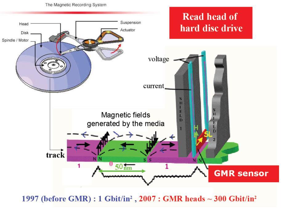
8 Magnetic field on nanoscale It is not difficult to get large fields going to nanometer scale. Giant magnetoresistance 8
9 Magnetoresistance in bulk Closed orbits: B-independent resistance Open orbits: MR ~ B 2 The MR effect has been of substantial importance technologically, especially in connection with read-out heads for magnetic disks and as sensors of magnetic fields. The most useful material has been an alloy between iron and nickel, Fe 20 Ni 80 (permalloy). The general consensus in the 1980s was that it was not possible to significantly improve performance of magnetic sensors based on MR. Giant magnetoresistance 9
 in Fe/Ge-O/Cojunctions at 4.2 K.")

10 Tunneling magnetoresistance Tunnel magnetoresistance (TMR) is a magnetoresistive effect that occurs in a magnetic tunnel junction (MTJ), which is a component consisting of two ferromagnets separated by a thin insulator. The effect was originally discovered in 1975 by M. Jullière (University of Rennes, France) in Fe/Ge-O/Cojunctions at 4.2 K. The relative change of resistance was around 14%, and did not attract much attention. In 1991 Terunobu Miyazaki (Tohoku University, Japan) found an effect of 2.7% at room temperature. Later, in 1994, Miyazaki found 18% in junctions of iron separated by an amorphous aluminum oxide insulator and Jagadeesh Moodera found 11.8% in junctions with electrodes of CoFe and Co. The highest effects observed to date with aluminum oxide insulators are around 70% at room temperature. By Fred the OysteriThe source code of this SVG is valid.this vector graphics image was created with Adobe Illustrator., GFDL, = Introduce effect of tunnelling magnetoresistance (TMR). What are the materials suitable for tunnelling magnetoresistance devices? Explain how TMR works and how to make tunnel magnetoresistance junctions. What are current and expected applications of TMR? Giant magnetoresistance 10
, CoFe / Al 2 O 3 /Co, Fe /Al 2 O 3 / Fe, Fe/MgO/Fe TMR can exceed 200% Due to the better performance of the magnetic tunnel junctions they are")
11 Tunneling magnetoresistance Here the insulator should be only a few atomic layers thick so that there is a significant probability that electrons can quantum mechanically tunnel through the insulating barrier Fe/amorphous Ge/Co, Ni/NiO/(Fe,Co,Ni), CoFe / Al 2 O 3 /Co, Fe /Al 2 O 3 / Fe, Fe/MgO/Fe TMR can exceed 200% Due to the better performance of the magnetic tunnel junctions they are expected to become the material of choice for technical applications. Their use for non-volatile magnetic random access memories (MRAM) is of particular interest - MRAM systems based on TMR are already on the market. One expects that TMR based technologies will become dominant over the GMR sensors. 4. Introduce effect of tunnelling magnetoresistance (TMR). What are the materials suitable for tunnelling magnetoresistance devices? Explain how TMR works and how to make tunnel magnetoresistance junctions. What are current and expected applications of TMR? Giant magnetoresistance 11
12 Spin polarization Spin interacts only weakly with its environment. The majority of the electron scattering events are spin-conserving, and it can therefore be expected that spin is conserved over distances that are much larger than the elastic mean free path. Key parameter in spintronics is spin polarization which could be defined as: and denote the majority and the minority spin, respectively. For q = 0, polarization P q = 1; while for q = q, P q = 0. TMR refers to the resistance of a ferromagnet insulator ferromagnet (FIF) tunnel junction in which coercive magnetic fields differ by a significant amount, which allows the relative orientation of the magnetizations to be changed by sweeping a magnetic field aligned parallel to the layers. It was found that, for the magnetizations of the two layers aligned parallel to each other, the tunnel resistance is lower than for antiparallel alignment. 5. What is spin polarization? Write its expression. What is effect of spin polarization on tunnelling magnetoresistance? Is tunnel resistance lower for antiparallel alignment of spins? Spintronics 12
13 Effect of spin polarization Magneto-resistance of a TMR structure formed by a CoFe Al 2 O 3 Co sandwich, with the magnetization directions of the two films as indicated in the schemes (bottom) Also shown in the top two traces are the much weaker anisotropic magnetoresistances of the corresponding individual films. The upper two curves show the small magnetoresistance changes in the two films (not the junction) which mark the coercive fields (H c ) by the position of their extrema. (The presence of a maximum or minimum is determined by the field and current directions.) The tunnel resistance is lower for parallel alignment. Spintronics 13
14 Conductance and polarization We define conductances Gp and Gap for the parallel and antiparallel configurations. The densities of states for the source and drain ferromagnetic electrodes are labeled D ( )S and D ( )D. Since, in a ferromagnet, D > D, we have Gp > Gap. The tunneling magnetoresistance (TMR) is usually defined as: Here R ap,p denotes the resistance of the corresponding configurations. Inserting the conductances gives: Here P denotes the polarization of the density of states. In cobalt, for example, P Co = 0.34, which gives a TMR of 0.26 in an ideal system. 6. Link conductance and polarization. How is tunnelling magnetoresistance (define it) expressed through the polarization of source and drain? Give an example of ideal TMR value for a metal, for instance, cobalt. Spintronics 14

15 TMR in memory chips In a magnetic random access memory (MRAM) chip, each bit is stored in a sequence of TMR layers. The lower ferromagnetic layer is hard, i.e. not reversible by the magnetic fields acting on the layers. The spin state of upper layer can be changed by current. The square arrays of TMR columns are contacted by one-dimensional arrays of wires on the top and on the bottom, which are rotated by 90 with respect to each other. In this way, each element of the array can be addressed individually. The writing, which means defining the orientation of the top magnetic layer, can be done by current pulses. The memory can be read out without a magnetic read head. Two states of the bit correspond to the two values of the measured current through tunnel junction. No moving parts are required. The stored data does not get lost when the power is turned off. 7. Explain how tunnelling magnetoresistance can be used in memory chips? Is hard ferromagnetic layer necessary in their construction? Is yes, why? How to assemble a sequence of TMR elements and how to write and read information? Are movable parts necessary? Are stored data lost when the power is turned off? Spintronics 15


16 TMR based memory chips Dynamic random-access memory Static random-access memory Spintronics 16

. In what systems does it take place?")
17 Giant magnetoresistance In GMR, as in TMR resistance depends on the relative orientation of the magnetizations of the ferromagnetic layers. Replace the insulator in a TMR layer sequence by a normal metal, and you have a GMR structure. It has been established that resistance dependence originates mostly from spin-dependent transmission of the conduction electrons across the ferromagnet normal metal interfaces. 8. Introduce phenomenon of giant magnetoresistance (GMR). In what systems does it take place? What are materials suitable for GMR devices and how are they used? What is the difference between GMR and TMR? Giant magnetoresistance 17


18 Giant magnetoresistance structures Fe/Cr/Fe trilayer, P. Grünberg, room temperature (FeCr)n, n=60. A. Fert, Liquid He temperature Giant magnetoresistance 18
. In what systems does it take place? What are materials suitable for GMR devices and how are they used?")
19 Giant magnetoresistance: two-current model The GMR effect as observed on a Fe Cr Fe sandwich structure. The anisotropic magnetoresistance of a ferromagnetic thin film is shown in comparison. Mott s two-current model 8. Introduce phenomenon of giant magnetoresistance (GMR). In what systems does it take place? What are materials suitable for GMR devices and how are they used? What is the difference between GMR and TMR? In the parallel configuration, the highly transmissive spin channel dominates the resistance; whereas, in the antiparallel configuration, both spin channels contribute equally to the resistance. This results in a lower overall resistance for the parallel configuration. Giant magnetoresistance 19
20 Density of states (DOS) profile Non-magnetic state: numbers of spin-up and spin-down electrons are equal Ferromagnetic state: numbers of spin-up and spin-down electrons are different Giant magnetoresistance 20

21 Physics of GMR Antiferromagnet trilayer system, H=0 Shown are DOS for upand down- spins Equivalent circuit diagram Magnetic field aligns the magnetic moments of the layers 12. Explain physics of GMR introducing equivalent circuit diagrams. What is the difference in resistance between parallel and antiparallel orientations? Is any way to enhance GMR using half-metals? Giant magnetoresistance 21


22 Spin aligned layers Ferromagnet trilayer system, H 0 Shown are DOS for upand down- spins Difference Giant magnetoresistance 22
23 A way to enhance GMR: Half-metals We are interested in the largest possible difference in the Fermi-level DOS for spin up and spin down. In half-metals the spin down band is metallic while the spin up band is an insulator (example CrO 2 ). Non-magnetic state Magnetic state Giant magnetoresistance 23


24 Half-metals GMR No electric current (spin blockade) Only spin down current Giant magnetoresistance 24

25 Ferromagnetic metals 3d transition metals - Fe, Co, Ni; lantanides (4f) - Gd The origin of magnetism - behavior of the 3d/4f electrons, respectively. We will focus on 3d elements. In the free atoms, the 3d and 4s levels of the 3d transition elements are hosts for the valence electrons. In the metallic state these 3d and 4s levels are broadened into energy bands. 4s orbitals are rather extended overlap between 4s orbitals of neighboring atoms 4s band is spread out over a wide energy range (15 20 ev). 3d orbitals are much less extended in space associated 3d energy band is comparatively narrow (4 7 ev). 4s electrons are much more mobile than 3d ones. 11. How do different spin states influence resistance of a material? How do 4d-electron states contribute to the resistance? What are requirements for building magnetic superlattices for GMR devices? How to engineer magnetic materials using principle of Friedel oscillations? How do electrons in non-magnetic layers provide coupling between magnetic layers? Giant magnetoresistance 25
26 Lowering energy of the state Energy of the state depends on the interplay between the (exchange) interaction between electrons and their kinetic energy. The Exchange Interaction: arises from Coulomb electrostatic interaction and the Pauli exclusion principle Higher repulsion energy Lower repulsion energy Giant magnetoresistance 26

27 Exchange interaction Exchange interaction requires overlap of wave functions. Giant magnetoresistance 27
28 Magnetic impurities Imperfections (defects and impurities) in metals become screened by the surrounding conduction electrons. The imperfection gives rise to decaying (Friedel) oscillations of the electron density as a function of the distance from the disruption. Similarly, a magnetic impurity atom in a metal gives rise to an induced spin polarization of the electron density. With increasing distance from the magnetic impurity there will be an oscillation in the sign of the polarization and the disturbance will also decay in magnitude with distance. As a consequence, the magnetic moment of a second impurity will become aligned parallel or antiparallel to the magnetic moment of the first moment depending on the sign of the induced polarization at that particular distance. Giant magnetoresistance 28
29 Mechanism of exchange interaction Localized spin induces spin polarization of conduction electrons. This polarization decays in space in an oscillatory fashion this is a property of magnetic susceptibility of the Fermi gas. Induced polarization interacts with second localized spin indirect exchange or RKKY (Ruderman-Kittel-Kasuya-Yosida) interaction. Depending on the distance, the RKKY interaction can be either ferromagnetic or antiferromagnetic! Electrons in non-magnetic layers provide coupling between magnetic layers! Giant magnetoresistance 29
30 Itinerant magnetism How much does it cost to create a FM state? A transfer of spin down electrons from the spin down band into the spin up band leads to lowering of the total energy (a gain). On the other hand, such a process requires a transfer of electrons from spin down levels below the initial Fermi energy, into spin up levels situated just above the initial Fermi energy. That will increase the total energy (a loss). Thus there is a competition between two opposite effects. This can be formulated as the so called Stoner criterion for ferromagnetism, J N (E F ) 1 Here J is called the Stoner exchange parameter and N(E F ) is the density of states at the Fermi energy. 10. Explain the concept of itinerant magnetism. Does itinerant magnetism important for giant magnetoresistance? In what materials does it takes place and what orbitals are most important for this effect? What role does exchange interaction play in itinerant magnetism? What is the Stoner criterion for ferromagnetism? Do you know a metal, which is on the verge of ferromagnetism? Giant magnetoresistance 30
31 Resistivity for different spin states Conductivity of d transition elements is mainly determined by the 4s electrons (easily mobile due to the wide 4s energy bands). However s electrons can scatter into the many d states which are available at the Fermi level considerable resistance. For Cu (following Ni in the Periodic Table) all the 3d states are situated below the Fermi level and therefore not available for scattering processes. This explains the particularly high conductivity of Cu. Sir Nevil Mott, 1936 In a ferromagnet like Fe there are 2 types of carriers, one made up from spin up electrons and one from spin down electrons. Since the density of states at the Fermi surface is quite different for the two spin states it follows that there is a significant difference in resistance for the spin up electrons and the spin down electrons. Giant magnetoresistance 31

32 Magnetic superlattices It is important that the lattice parameters for the different layers match each other; it is also an advantage if the two metals forming the superlattice have the same crystal structure. This is the case for Cr and Fe, where both metals adapt the bcc crystal structure and have very similar lattice spacing. It was also extremely important that the spatial separation between the magnetic layers is of the order of nanometers. In order to exhibit the GMR effect the mean free path for the conduction electrons has to greatly exceed the interlayer separations so that the electrons can travel through magnetic layers and pick up the GMR effect. Giant magnetoresistance 32

33 Preparation of superlattices Key ingredients MBE Growth of metallic multilayers Novel characterization methods At present time, GMR structures can be also obtained by magnetron sputtering Giant magnetoresistance 33


34 GMR effect and applications A prerequisite for the discovery of the GMR-effect was provided by the new possibilities of producing fine layers of metals on the nanometer scale. Originally, epitaxy was used. At present time, after Stuart Parkin, more simple and cheap method sputtering is more practical. GMR effect can also be observed when the current flows parallel to the layers. One speaks of the current perpendicular to plane (CPP) and the current in plane (CIP) configurations. In spite being much weaker, CIP is an important configuration, since CPP has very small overall resistance. 13. Can GMR effect be observed when the current flows parallel to the layers? Explain physics of it. What are currentperpendicular-to-plane (CPP) and the current-in-plane (CIP) configurations? Why is CIP important? Giant magnetoresistance 34


35 Spin injection The current density across the interface between a ferromagnet (F) and a normal conductor (N), is composed of two spin components, j = j + j. The spin current density is given by js = j j. Here, we denote by the majority spin in the ferromagnet. In a normal conductor, there is no spin current associated with a charge current. In the centre of normal conductor: Close to interface: β N is the fraction of the current density carried by the spin-up channel in the normal metal. 14. Outline principles of spin injection. Describe spin transport in ferromagnet and spin accumulation close to interface with normal metal. Introduce spin-flip scattering time and spin relaxation length. Describe these processes in specific materials. Giant magnetoresistance 35
36 Spin injection: spin transport in ferromagnet In the ferromagnet, the two spin directions experience different conductivities: Here denote the spin-resolved densities of states at the Fermi energy and the diffusion constants, respectively, while α F represents the fraction of the total ferromagnet conductance that is contributed by the spin up channel. The current in ferromagnet is split among the spin channels: Here β F is the fraction of the current density carried by the spin-up channel in the ferromagnet. Because in the normal metal, spin channels have equal conductances and in ferromagnet not, the spin accumulates close to the interface, and a spin density gradient builds up in both materials. This means that, in the interface region, the two spin directions have different electrochemical Potentials with and. Giant magnetoresistance 36
37 Spin injection: diffusion equation By introducing spin-flip scattering times: the diffusion equation can be obtained Here n F ( ) denotes the spin-resolved electron densities, T (T ) are the spin-flip scattering times from into (respectively, from into ) and T 1F is the spin relaxation time Diffusion equation: Diffusion equation solution: Here λ F(N) is the spin relaxation length in the corresponding material. Giant magnetoresistance 37
38 Spin injection: properties of interface By solving current equations on both sides of interface and equalling currents, one can obtain: Spin accumulation at the ferromagnet normal metal interface, expressed in terms of the spin-resolved electrochemical potentials. The step of the averaged electrochemical potentials across the interface is denoted by Δμ. For a ferromagnet with P jf = 1, the spins are perfectly injected into the normal metal! To aim for a large spin polarization in the normal conductor, (λ N /σ N )/(λ F /σ F ) should be as small as possible. 15. How are chemical potentials of differently polarized electrons linked in the interface? Write expression for the current polarization at an ferromagnet-normal metal interface. What is the condition of perfect injection of spins? Giant magnetoresistance 38
39 Spin injection: experiments A spin-polarized current is injected from permalloy (Ni 80 Fe 20 ) into copper, and a value of P j,cu = 0.02 was extracted. A spinflip time T 1,Cu of 42 ps was found at 4.2K, which corresponds to λ Cu 1 μm. Since the Drude scattering time in copper is 30 fs at 4.2K, these results show that the electrons experience 1000 elastic scattering events on average before they experience a spin flip. Even at room temperature, a relatively large value of λ Cu 350 nm remains. Spintronics 39
40 Colossal magnetoresistance Colossal magnetoresistance (CMR) is a property of some materials, mostly manganese-based perovskite oxides, that enables them to dramatically change their electrical resistance in the presence of a magnetic field. The magnetoresistance of conventional materials enables changes in resistance of up to 5%, but materials featuring CMR may demonstrate resistance changes by orders of magnitude. This technology may find uses in disk read-and-write heads, allowing for increases in hard disk drive data density. La 0.67 Ca 0.33 MnO 3 La 0.67 Sr 0.33 MnO 3 T Curie = 250 K T Curie = 350 K CMR materials are perovskites with crystal lattice that is very close to crystal lattice of hightemperature superconductors, for example, YBa 2 Cu 3 O x. Y Tokura, Critical features of colossal magnetoresistive manganites, Reports on Progress in Physics, Volume 69, Number 3, p (2006).
41 Spin injection into YBa 2 Cu 3 O x 5 I H 1 E F CMR HTS 1 - STO substrate (5 mm 5 mm); 2 - YBCO; 3 - STO barrier; 4 - CMR; 5 - gold contact pads. The arrow shows the direction of the applied field.
42 Current dependence of the effect of spin injection 5 t (min.) I (ma) m (10-8 Am 2 ) m (10-8 Am 2 ) I = ma t (min.) p =1 s
43 Interaction with antiferromagnetic spin fluctuations: annealing experiments R (Ohm) YBCO R /R 290K T (K) , 3 h 350, 3 h 350 C, 10 h C, 24 h C, 24 h C, 48 h C, 96 h T (K) The annealing experiments, which change T* and the upper boundary of AFM spin fluctuations, display the removal of increase in resistance and coercive field effect. I 1 V 1 Au YBCO YBCO/LCMO&Au interface Au V 2 I 2 R/R 0 Amplitude (10-2 a.u.) C8_ K 68.9 K 73.5 K 78.3 K 87.4 K 89.2 K K K Annealed H (Oe) YBCO/LCMO As prepared T (K) Exposed, 7 months T Curie
44 Spin injection into ultrathing films K I 1 V 1 V 2 I 2 Au YBa 2 Cu 3 O x I (ma) K The bilayer is set in the resistive state V (mv) I 1 V 1 V 2 I 2 La 0.7 Ca 0.3 MnO 3 SrTiO 3 substrate YBCO film: nm Quasiparticle exchange has a considerable ab-plane component
45 Spin injection into ultrathing films V (10-4 V) R (Ohm) K 72.7 K YBCO d = 25 nm H (a.u.) 74.7 K V (%) T (K) m (A m 2 ) Data: EffectPercent_B Model: Gauss Equation: y=y0 + (A/(w*sqrt(PI/2)))*exp(-2*((x-xc)/w)^2) Weighting: y No weighting Chi^2/DoF = R^2 = H (Oe) y0 0 ±0 xc ± w ± A ± xc ± w ± A ± Minimums dissapear here T (K) Both low-temperature and close-to-t c effects of spin injection are observed in ultrathing films
46 4-corners transport measurements V 1.8 V 0.3 V 5.0 V V V Resistance ( ) Resistance ( ) Temperature (K) Temperature (K) I Montgomery technique I


47 Superconductivity: seeing is believing Faraday effect and magneto-optical imaging Michael Faraday, 1842, by Thomas Phillips The Faraday effect is a rotation of the polarization of light in presence of magnetic field. The effect was discovered by Michael Faraday in

48 Magneto-optical study A differential MOI image showing the in- plane magnetization of the LCMO thin film surface. The sample is covered with an MO-indicator film and the red line indicates where the sample ends. The contrast in the image represents areas of strong and weak magnetic fields periodically alternating in the plane of the film and seen as bright and dark areas, respectively.

, 10-15 September 2017,")
49 2500 Anisotropy transport measurements parallel perpendicular V V Resistance ( Resistance ( Temperature (K) I I Temperature (K), September 2017, Zatoka, Ukraine


50 Scanning electron microscopy and EDX YBa 2 Cu 3 O 7-d 500 nm La 0.67 Ca 0.33 MnO 3 Mn-KA 500 nm 500 nm Scanning electron microscopy and EDX confirm presence of both layers with reasonably well defined interface., September 2017, Zatoka, Ukraine
51 X-ray diffraction study Thickness fringe SrTiO 3 log 10 (intensity [a.u.]) Unknown phase LCMO/ YBCO Angle [degrees] The main peak in x-ray diffraction scan is from the SrTiO 3 -substrate. LCMO and YBCO are also identified in the scan. In addition, there are some unknown peaks that indicate significant interdiffusion between the LCMO and YBCO forming interface layer with different properties than those of the pure compounds., September 2017, Zatoka, Ukraine
52 Magnetization measurements m (10-4 emu) ZFCW 1 T FCW 1 T FCC 1 T T(K)

53 Interface magnetism J. Chakhalian et al., Magnetism at the interface between ferromagnetic and superconducting oxides, Nature Physics 2, 244 (2006). Carefully controlled interfaces between two materials can give rise to novel physical phenomena and functionalities not exhibited by either of the constituent materials alone. Here we examine superlattices composed of the halfmetallic ferromagnet La 2/3 Ca 1/3 MnO 3 and the hightemperature superconductor YBa 2 Cu 3 O 7 by absorption spectroscopy with circularly polarized X-rays and by off-specular neutron reflectometry. The resulting data yield microscopic insight into the interplay of spin and orbital degrees of freedom at the interface. The experiments also reveal an extensive rearrangement of the magnetic domain structure at the superconducting transition temperature.
54 An ex-situ YBCO/LCMO bilayer was investigated by a range of techniques. A strong anisotropy in resistance and a resistance peak is observed below critical temperature of superconductor. The resistance peak corresponds to stripy magnetic structure seen by magneto-optical imaging and registered by vibrating sample magnetometry. It is suggested that magnetic structure is associated with YBCO/LCMO interface., September 2017, Zatoka, Ukraine

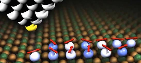
55 Evidence of spin injection from La 0.67 Ca 0.33 MnO 3 to YBa 2 Cu 3 O x T. B. Hjelmeland et al. V 1 V 2 1,0 0,8 Spin Injection No Spin Injection Difference 1,0 0,8 Spin Injection No Spin Injection Difference R[Ohm] 0,6 0,4 R[Ohm] 0,6 1 V 3 V 0,4 0,2 0,2 0,0 0, T[K] T[K] I 1 I 2 I 2 R[Ohm] 1,0 0,8 0,6 0,4 Spin Injection No Spin Injection Difference 9 V R[Ohm] 1,0 0,8 0,6 0,4 Spin Injection No Spin Injection Difference 15 V 0,2 0,2 0,0 0, T[K] T[K] Spin injection is most effective close to T c Giant magnetoresistance 55
56 R (Ohm) I 1 Evidence of spin injection from La 0.67 Ca 0.33 MnO 3 to YBa 2 Cu 3 O x V 1 V 2 I 2 V T (K) 1 V 3 V 6 V 9 V 12 V 15 V V 2 R (Ohm) I [A] 0,016 0,014 0,012 0,010 0,008 0,006 0,004 0,002 0, T [K] T. B. Hjelmeland et al T (K) V 2 Spin injection in normal state of YBa 2 Cu 3 O x is revealed. 1 V 3 V 6 V 9 V 12 V 15 V Giant magnetoresistance 56


 1 V 3 V 6 V 9 V")
 YBCO Spin injection in")
57 Evidence of spin injection from La 0.67 Ca 0.33 MnO 3 to YBa 2 Cu 3 O x V 1 V 2 0,6 0,4 T. B. Hjelmeland et al. Straight line is subtracted, two measurement configurations YBCO LCMO R (Ohm) I I 2 I T (K) 1 V 3 V 6 V 9 V 12 V 15 V R(Ohm) 0,2 0,0-0,2 1 V 1 V 3 V 3 V 9 V 9 V 15 V 15 V T(K) YBCO Spin injection in normal state of YBa 2 Cu 3 O x is revealed. Giant magnetoresistance 57
 Spin-polarized electrons are injected in the semiconductor Ferromagnetic drain contact is used as analyzer Idea by Datta & Das Not realized experimentally Gate is used to rotate the")
58 Datta Das spin transistor Spin FET is a modification of a GMR structure. S. Datta and B. Das, Appl. Phys. Lett. 56, 665 (1990) Spin-polarized electrons are injected in the semiconductor Ferromagnetic drain contact is used as analyzer Idea by Datta & Das Not realized experimentally Gate is used to rotate the polarization plane (Rashba effect) No need to add/remove electrons less energy consumption! 16. Introduce concept of Datta Das spin transistor. Is it implemented? Does it use semiconductor? What are difficulties in injecting spins into semiconductor and what are possible solutions to overcome these difficulties? How can additional interface resistance in a tunnel barrier structure increase injected spin polarization? Spintronics 58
59 Spin injection into semiconductors It is difficult task because conductivity is lower than that of the ferromagnet and the spin-flip length is longer. Two possible solutions: a) a ferromagnet with a spin polarization of P jf = 1, b) inserting tunnel barriers at the ferromagnet semiconductor interface to use spin-selective interface resistance. Interface tunnel barriers Additional interface resistance R i ( ) depends on spin and makes the spinresolved electrochemical potentials discontinuous at the interface. Giant magnetoresistance 59
60 Detection of spin-polarized current A frequently used technique is based on conversion of the spin polarization into circular polarization of photons, for example by a LED p n type junction. During electron hole recombination, the dipole selection rules allow only transitions between electron and hole states that emit photons of left or right circular polarization, with a weight given by the corresponding dipole matrix elements. σ+ (σ ) polarization of 0.5 Selection rules for photon emission by electron hole recombination in GaAs. The relative intensities and the orientation of the circular polarization are indicated at each transition. The circularly polarized emitted light reflects the spin polarization of the injected current. P j = 0.13 at the GaAs quantum well at a temperature of 4K is found, which decayed to 0.04 at 240K. The injected polarization at the interface was estimated to be as high as P j = 0.3 and independent of the temperature. 17. How to detect spin-polarized current? Has it anything to do with circular polarization of photons? Can LED p n type junctions be used for that? Please explain how. Do you know any spin-polarization experiments involving GaAs quantum wells? What polarization was observed there? Giant magnetoresistance 60
61 Ferromagnetic semiconductors The Fermi energy in semiconductors is small compared to that in metals, and can become smaller than the spin splitting of the conduction band. This results in a spin polarization of 1. Consequently, the impedance mismatch problem would not occur. The remanence and the coercive magnetic field could be tuned by a gate voltage. A significant circular polarization of the emitted light is detected. Spin injection from a ferromagnetic semiconductor into a GaAs quantum well. Magnetization hysteresis curves of Ga 1 x Mn x As. A spin polarization of the current injected from Ga 1 x Mn x As into GaAs of P j = 0.82 at liquid helium temperatures has been found. The impedance mismatch problem has been solved, at least conceptually. 18. What are ferromagnetic semiconductors? Do they help to solve the impedance mismatch problem? Can they have spin polarization equal to 1? How it can be achieved? Can Ga1 xmnxas be used as a ferromagnetic semiconductor? What are the results of experiments with this compound? Giant magnetoresistance 61
 is formed.")
62 Rashba effect The Rashba effect denotes the spin orbit coupling experienced by moving electrons in electric fields. It can be induced by macroscopic electric field in a semiconductor quantum well. Due to the band offsets at the interface of two different materials the electrons are confined in a quantum well. A two-dimensional electron gas (2DEG) is formed. If the potential well is asymmetric, the electrons are moving in an effective electric field E. In the reference system of the electron this electrical field transforms into a magnetic field B. Depending of the spin orientation and the corresponding magnetic moment an energy lowering or an energy increase occurs, respectively. For applications it is essential, that the strength of the Rashba effect and thus the spin splitting can be controlled by means of a gate electrode. 19. What is Rashba effect? Can you explain its origin? Do you know any experimental observations of the Rashba effect? How could this effect be used in spin based field-effect transistor? What are the conditions for constructing Datta Das transistor? Spintronics 62

63 Derivation of Rashba effect The Rashba effect is a direct result of inversion symmetry breaking in the direction perpendicular to the two-dimensional plane. Therefore, let us add to the Hamiltonian a term that breaks this symmetry in the form of an electric field Due to relativistic corrections an electron moving with velocity v in the electric field will experience an effective magnetic field B This magnetic field couples to the electron spin where is the magnetic moment of the electron. Within this toy model, the Rashba Hamiltonian is given by: The eigenvalues are: The energy dispersion of a free 2DEG in an In 0.53 Ga 0.47 As In 0.52 Al 0.48 As quantum well with η = ev m and m 0.05m e, with the Rashba effect taken into account. The arrows depict the corresponding spin directions. Spintronics 63
64 Observation of Rashba effect For a Fermi energy of E F = 10 mev and a spin orbit coupling constant η = ev m, we find Δk F = m k F. It corresponds to a modulation of certain wavelength. Modulation of Shubnikov de Haas oscillations due to the Rashba effect. This is a rotation along a circle formed by the intersection of the Bloch sphere with the plane given by φ. In real space, the spinor rotates around the direction of the magnetic field seen by the electron, i.e. around the axis in the (x, y) plane that is perpendicular to k. For the above values, we find from Δk F L = 2 a rotation about over a distance L. The Datta Das transistor only works when the spin directions are well defined, which means that the channel should be quasi-one-dimensional. Second, the channel should be ballistic. Even though elastic scattering does not flip the spin, it changes the continuous spin rotation abruptly. Spintronics 64
65 Spin relaxation and spin dephasing One has to distinguish between two different time scales. First time scale T 1 comes from spin-up state experiencing a spin-flip scattering event and ending up in a spin-down state (or vice versa). Second time scale T 2 refers to the loss of the correlation of the spin precession around the quantization axis when it moves with the Larmor frequency ω L = eb/2m around the effective magnetic field axis. It is also the time over which the superposition of two states, a situation encountered frequently in quantum computational schemes, decays into a pure state. In Elliot Yafet (EY) spin orbit coupling mechanism, even spin-independent interactions can induce transitions between these eigenstates and generate spin dephasing. This type of spin relaxation increases both with the spin orbit coupling and electron scattering rate. In GaAs, Elliot Yafet spin relaxation is very strong for holes due to large spin orbit coupling. The Dyakonov Perel (DP) mechanism emerges from the fact that the spin degeneracy is lifted in crystals without inversion symmetry. In contrast to the Elliot Yafet mechanism, the dephasing occurs not during the scattering but during the electron motion in between these events. Because of this, the spin relaxation time is inversely proportional to the Drude scattering time. By studying the spin relaxation time as a function of the mobility, one can easily distinguish between Elliot Yafet and Dyakonov Perel mechanisms. Spintronics E is the energy of the electron and Δ SO is the spin orbit splitting. 20. Introduce spin relaxation and spin dephasing times. What mechanisms of spin relaxation do you know? What is their dependence on Drude scattering time? 65


66 Hyperfine interaction It is an important source of spin relaxation, in which the spin-polarized electron gas interacts with the nuclear spins via H IS polarizing the nuclei while experiencing spin relaxation itself. It has been calculated that. This means that hyperfine interactions are particularly important at low carrier densities. In a confined system like a ballistic quantum dot, the first two mechanisms, which rely on extended motion of the electrons, should be of minor importance, while the hyperfine interaction remains relevant. This is an important factor and the reason why extremely long spin relaxation times can be observed in such systems. 21. Explain hyperfine interaction. Where does it take place and what is its importance in spin systems? In what devices could it be most efficient? What are possible applications of hyperfine interaction? Spintronics 66
67 Recent developments Magnetic semiconductors (quick performance) Spin injection from a metallic ferromagnet into a semiconductor from a magnetic semiconductor to a non-magnetic semiconductor Magnetic switching induced by spin currents The discovery of GMR opened the door to a new field of science, magnetoelectronics (or spintronics), where two fundamental properties of the electron, namely its charge and its spin, are manipulated simultaneously. Emerging nanotechnology was an original prerequisite for the discovery of GMR, now magnetoelectronics is in its turn a driving force for new applications of nanotechnology. 22. Name few modern spintronics trends and explain their importance. Do you aware of spintronics aspects in graphene and topological insulators (TIs)? Is single molecule GMR possible? Spintronics 67


68 Recent STM developments Atom-by-atom engineering and magnetometry of tailored nanomagnets Roland Wiesendanger et al., Institute of Applied Physics, Hamburg University, Jungiusstrasse 11, D Hamburg, Germany Experiments were performed in an ultrahigh vacuum scanning tunnelling microscope at a temperature of T 0.3 K with a magnetic field B up to 12 T applied perpendicular to the sample surface. Spin-polarized Fe atoms on Cu. Spintronics 68
69 Spintronics (abbreviation for Spin Transport Electronics") is an emerging technology exploiting both the intrinsic spin of the electron and its associated magnetic moment, in addition to its fundamental electronic charge, in solid-state devices. New ingredients Spintronics trends 1. current-induced torque (CIT), also known as the spin-transfer torque. The manipulation of magnetization by CITs has its origin in angular momentum conservation, which twists the layer receiving the angular momentum carried by the spin current. Spin is a key element for the next-generation magnetic random access memories, logic-in-memory architectures, and high-density memory devices. Spin-torque-based nano-oscillators can be exploited as tunable microwave generators in wireless device technology, as well as a means of low-power spin-wave interconnects in logic devices. Spintronics 69
70 Spintronics trends 2. The second is the spin Hall effect (SHE), which originates from the relativistic spin orbit coupling (SOC) interaction that turns the electrons perpendicular to the current in a spin-dependent way. Despite the short time since its discovery, SHE has now become a standard tool in the detection of spin currents and spin polarization. It has been used to create one of the first spin field-effect transistors (FETs), to measure spin currents generated by magnetization dynamics, and even to generate spin currents large enough to produce spin-torque effects. 3. The third subfield is spin caloritronics. Envisaged in an early work on spin injection and ignited by the discovery of the spin Seebeck effect, thermal gradients driving heat currents are now being exploited to generate spin currents. The origin of the effect seems to be the coupling between collective spin modes (magnons) and lattice excitations (phonons). The spin dependence of the heat conductance, Seebeck and Peltier effect may have important energy applications. Spintronics 70
71 Spintronics trends 4. The fourth is silicon spintronics. Silicon is not only abundant (its oxide is sand) and the central material for electronics, but it also has very desirable long spin-relaxation times. It was a late bloomer in spintronics, mostly because its indirect band gap and weak SOC have, for decades, precluded spin injection and detection. Recent experimental breakthroughs have, however, demonstrated that the electron spin in silicon can be reliably injected and detected as well as transferred over relatively large distances, allowing a seamless integration with electronic circuits, such as connecting close-by processor cores. 5. Finally, the fifth entails the spintronic aspects of graphene and topological insulators (TIs), which originate from the bandstructure properties and create an effective topological knot. This property protects the states of graphene or the surface states of a TI from non-magnetic disorder effects. Spintronics 71

72 Silicon based spin transistor A ferromagnetic emitter to inject spinpolarized electrons via a tunnel barrier into a silicon base These spin-polarized minority carriers traverse the base diffusively and are harvested by the ferromagnetic collector via another tunnel barrier The spin selectivity derives from the back-biased collector presenting a different density of final spin states to the spin-polarized minority carriers in the base. Spintronics 72
 molecules adsorbed onto two Co")

73 GMR through a single molecule H 2 Pc (hydrogen phthalocyanine) molecules adsorbed onto two Co islands on the Cu(111) surface. Magnetoresistance 51% Schmaus et al., cond-mat 2011 Giant magnetoresistance 73


74 Quantum devices (qubits and gates) A SEM image of a double quantum dot A SEM image of a two qubit device Having nanosecond resolution one have to use a lot of high frequency components, which must all work at 40 millikelvin. Here is a picture of a board with a sample on it. There is a microwave stripline for four coaxial cables to bring high frequency signals to the sample 23. In what quantum devices could spin be used? Can it be relevant to quantum computing? What are other emerging applications of spintronics? What problems need to be solved in this area? Spintronics 74
75 Electronics applications Spintronics 75
76 Problems Spin injection in semiconductor optimizing interfaces and materials are needed. - one of ways using magnetic semiconductors as FM decreases impedance mismatch Gate-induced spin rotation (Rashba effect) Spin relaxation and decoherence Spintronics is a new emerging field providing promising solutions for signal processing and realization of computer algorithms. Spin depolarization is still large many things have to be done to make coherent spintronics practical. Current induced magnetisation switch Spintronics 76
Mesoscopic Spintronics
 Mesoscopic Spintronics Taro WAKAMURA (Université Paris-Sud) Lecture 1 Today s Topics 1.1 History of Spintronics 1.2 Fudamentals in Spintronics Spin-dependent transport GMR and TMR effect Spin injection
Ferromagnetism and Electronic Transport. Ordinary magnetoresistance (OMR)
") Ferromagnetism and Electronic Transport There are a number of effects that couple magnetization to electrical resistance. These include: Ordinary magnetoresistance (OMR) Anisotropic magnetoresistance (AMR)
Ferromagnetism and Electronic Transport There are a number of effects that couple magnetization to electrical resistance. These include: Ordinary magnetoresistance (OMR) Anisotropic magnetoresistance (AMR)
MAGNETORESISTANCE PHENOMENA IN MAGNETIC MATERIALS AND DEVICES. J. M. De Teresa
 MAGNETORESISTANCE PHENOMENA IN MAGNETIC MATERIALS AND DEVICES J. M. De Teresa Instituto de Ciencia de Materiales de Aragón, Universidad de Zaragoza-CSIC, Facultad de Ciencias, 50009 Zaragoza, Spain. E-mail:
SPINTRONICS. Waltraud Buchenberg. Faculty of Physics Albert-Ludwigs-University Freiburg
 SPINTRONICS Waltraud Buchenberg Faculty of Physics Albert-Ludwigs-University Freiburg July 14, 2010 TABLE OF CONTENTS 1 WHAT IS SPINTRONICS? 2 MAGNETO-RESISTANCE STONER MODEL ANISOTROPIC MAGNETO-RESISTANCE
Spins and spin-orbit coupling in semiconductors, metals, and nanostructures
 B. Halperin Spin lecture 1 Spins and spin-orbit coupling in semiconductors, metals, and nanostructures Behavior of non-equilibrium spin populations. Spin relaxation and spin transport. How does one produce
Giant Magnetoresistance
 Giant Magnetoresistance N. Shirato urse: Solid State Physics 2, Spring 2010, Instructor: Dr. Elbio Dagotto Department of Materials Science and Engineering, University of Tennessee, Knoxville, TN 37996
Chapter 3 Properties of Nanostructures
 Chapter 3 Properties of Nanostructures In Chapter 2, the reduction of the extent of a solid in one or more dimensions was shown to lead to a dramatic alteration of the overall behavior of the solids. Generally,
μ (vector) = magnetic dipole moment (not to be confused with the permeability μ). Magnetism Electromagnetic Fields in a Solid
 = magnetic dipole moment (not to be confused with the permeability μ). Magnetism Electromagnetic Fields in a Solid") Magnetism Electromagnetic Fields in a Solid SI units cgs (Gaussian) units Total magnetic field: B = μ 0 (H + M) = μ μ 0 H B = H + 4π M = μ H Total electric field: E = 1/ε 0 (D P) = 1/εε 0 D E = D 4π P
Magnetism Electromagnetic Fields in a Solid SI units cgs (Gaussian) units Total magnetic field: B = μ 0 (H + M) = μ μ 0 H B = H + 4π M = μ H Total electric field: E = 1/ε 0 (D P) = 1/εε 0 D E = D 4π P
Solid Surfaces, Interfaces and Thin Films
 Hans Lüth Solid Surfaces, Interfaces and Thin Films Fifth Edition With 427 Figures.2e Springer Contents 1 Surface and Interface Physics: Its Definition and Importance... 1 Panel I: Ultrahigh Vacuum (UHV)
Advanced Lab Course. Tunneling Magneto Resistance
 Advanced Lab Course Tunneling Magneto Resistance M06 As of: 015-04-01 Aim: Measurement of tunneling magnetoresistance for different sample sizes and recording the TMR in dependency on the voltage. Content
Giant Magnetoresistance
 GENERAL ARTICLE Giant Magnetoresistance Nobel Prize in Physics 2007 Debakanta Samal and P S Anil Kumar The 2007 Nobel Prize in Physics was awarded to Albert Fert and Peter Grünberg for the discovery of
Current-driven Magnetization Reversal in a Ferromagnetic Semiconductor. (Ga,Mn)As/GaAs/(Ga,Mn)As Tunnel Junction
As/GaAs/(Ga,Mn)As Tunnel Junction") Current-driven Magnetization Reversal in a Ferromagnetic Semiconductor (Ga,Mn)As/GaAs/(Ga,Mn)As Tunnel Junction D. Chiba 1, 2*, Y. Sato 1, T. Kita 2, 1, F. Matsukura 1, 2, and H. Ohno 1, 2 1 Laboratory
Current-driven Magnetization Reversal in a Ferromagnetic Semiconductor (Ga,Mn)As/GaAs/(Ga,Mn)As Tunnel Junction D. Chiba 1, 2*, Y. Sato 1, T. Kita 2, 1, F. Matsukura 1, 2, and H. Ohno 1, 2 1 Laboratory
From Hall Effect to TMR
 From Hall Effect to TMR 1 Abstract This paper compares the century old Hall effect technology to xmr technologies, specifically TMR (Tunnel Magneto-Resistance) from Crocus Technology. It covers the various
Some pictures are taken from the UvA-VU Master Course: Advanced Solid State Physics by Anne de Visser (University of Amsterdam), Solid State Course
, Solid State Course") Some pictures are taken from the UvA-VU Master Course: Advanced Solid State Physics by Anne de Visser (University of Amsterdam), Solid State Course by Mark Jarrel (Cincinnati University), from Ibach and
Some pictures are taken from the UvA-VU Master Course: Advanced Solid State Physics by Anne de Visser (University of Amsterdam), Solid State Course by Mark Jarrel (Cincinnati University), from Ibach and
Recent developments in spintronic
 Recent developments in spintronic Tomas Jungwirth nstitute of Physics ASCR, Prague University of Nottingham in collaboration with Hitachi Cambridge, University of Texas, Texas A&M University - Spintronics
Saroj P. Dash. Chalmers University of Technology. Göteborg, Sweden. Microtechnology and Nanoscience-MC2
 Silicon Spintronics Saroj P. Dash Chalmers University of Technology Microtechnology and Nanoscience-MC2 Göteborg, Sweden Acknowledgement Nth Netherlands University of Technology Sweden Mr. A. Dankert Dr.
Physics and applications (I)
") Spintronics: Physics and applications (I) Malek Zareyan IPM, 15 TiR 1387 1 Very weak magnetic changes give rise to major differences in resistance in a GMR system (.( ١٩٨٨ GMR has made possible miniaturizing
Spintronics: Physics and applications (I) Malek Zareyan IPM, 15 TiR 1387 1 Very weak magnetic changes give rise to major differences in resistance in a GMR system (.( ١٩٨٨ GMR has made possible miniaturizing
introduction: what is spin-electronics?
 Spin-dependent transport in layered magnetic metals Patrick Bruno Max-Planck-Institut für Mikrostrukturphysik, Halle, Germany Summary: introduction: what is spin-electronics giant magnetoresistance (GMR)
The Physics of Ferromagnetism
 Terunobu Miyazaki Hanmin Jin The Physics of Ferromagnetism Springer Contents Part I Foundation of Magnetism 1 Basis of Magnetism 3 1.1 Basic Magnetic Laws and Magnetic Quantities 3 1.1.1 Basic Laws of
From nanophysics research labs to cell phones. Dr. András Halbritter Department of Physics associate professor
 From nanophysics research labs to cell phones Dr. András Halbritter Department of Physics associate professor Curriculum Vitae Birth: 1976. High-school graduation: 1994. Master degree: 1999. PhD: 2003.
Electron spins in nonmagnetic semiconductors
 Electron spins in nonmagnetic semiconductors Yuichiro K. Kato Institute of Engineering Innovation, The University of Tokyo Physics of non-interacting spins Optical spin injection and detection Spin manipulation
Spintronics at Nanoscale
 Colloquium@NTHU Sep 22, 2004 Spintronics at Nanoscale Hsiu-Hau Lin Nat l Tsing-Hua Univ & Nat l Center for Theoretical Sciences What I have been doing Spintronics: Green s function theory for diluted magnetic
VALLIAMMAI ENGINEERING COLLEGE
 VALLIAMMAI ENGINEERING COLLEGE SRM Nagar, Kattankulathur 603 203 DEPARTMENT OF PHYSICS QUESTION BANK II SEMESTER PH8252 - PHYSICS FOR INFORMATION SCIENCE (Common to CSE & IT) Regulation 2017 Academic Year
Challenges for Materials to Support Emerging Research Devices
 Challenges for Materials to Support Emerging Research Devices C. Michael Garner*, James Hutchby +, George Bourianoff*, and Victor Zhirnov + *Intel Corporation Santa Clara, CA + Semiconductor Research Corporation
Spin electronics at the nanoscale. Michel Viret Service de Physique de l Etat Condensé CEA Saclay France
 Spin electronics at the nanoscale Michel Viret Service de Physique de l Etat Condensé CEA Saclay France Principles of spin electronics: ferromagnetic metals spin accumulation Resistivity of homogeneous
Spin caloritronics in magnetic/non-magnetic nanostructures and graphene field effect devices Dejene, Fasil
 University of Groningen Spin caloritronics in magnetic/non-magnetic nanostructures and graphene field effect devices Dejene, Fasil DOI: 10.1038/nphys2743 IMPORTANT NOTE: You are advised to consult the
Neutron and x-ray spectroscopy
 Neutron and x-ray spectroscopy B. Keimer Max-Planck-Institute for Solid State Research outline 1. self-contained introduction neutron scattering and spectroscopy x-ray scattering and spectroscopy 2. application
CHAPTER 2 MAGNETISM. 2.1 Magnetic materials
 CHAPTER 2 MAGNETISM Magnetism plays a crucial role in the development of memories for mass storage, and in sensors to name a few. Spintronics is an integration of the magnetic material with semiconductor
What so special about LaAlO3/SrTiO3 interface? Magnetism, Superconductivity and their coexistence at the interface
 What so special about LaAlO3/SrTiO3 interface? Magnetism, Superconductivity and their coexistence at the interface Pramod Verma Indian Institute of Science, Bangalore 560012 July 24, 2014 Pramod Verma
Spintronics. Seminar report SUBMITTED TO: SUBMITTED BY:
 A Seminar report On Spintronics Submitted in partial fulfillment of the requirement for the award of degree of Electronics SUBMITTED TO: SUBMITTED BY: www.studymafia.org www.studymafia.org Preface I have
TRANSVERSE SPIN TRANSPORT IN GRAPHENE
 International Journal of Modern Physics B Vol. 23, Nos. 12 & 13 (2009) 2641 2646 World Scientific Publishing Company TRANSVERSE SPIN TRANSPORT IN GRAPHENE TARIQ M. G. MOHIUDDIN, A. A. ZHUKOV, D. C. ELIAS,
EXTRINSIC SEMICONDUCTOR
 EXTRINSIC SEMICONDUCTOR In an extrinsic semiconducting material, the charge carriers originate from impurity atoms added to the original material is called impurity [or] extrinsic semiconductor. This Semiconductor
Metals: the Drude and Sommerfeld models p. 1 Introduction p. 1 What do we know about metals? p. 1 The Drude model p. 2 Assumptions p.
 Metals: the Drude and Sommerfeld models p. 1 Introduction p. 1 What do we know about metals? p. 1 The Drude model p. 2 Assumptions p. 2 The relaxation-time approximation p. 3 The failure of the Drude model
2 B B D (E) Paramagnetic Susceptibility. m s probability. A) Bound Electrons in Atoms
 Paramagnetic Susceptibility. m s probability. A) Bound Electrons in Atoms") Paramagnetic Susceptibility A) Bound Electrons in Atoms m s probability B +½ p ½e x Curie Law: 1/T s=½ + B ½ p + ½e +x With increasing temperature T the alignment of the magnetic moments in a B field is
Paramagnetic Susceptibility A) Bound Electrons in Atoms m s probability B +½ p ½e x Curie Law: 1/T s=½ + B ½ p + ½e +x With increasing temperature T the alignment of the magnetic moments in a B field is
Physics of Semiconductors
 Physics of Semiconductors 13 th 2016.7.11 Shingo Katsumoto Department of Physics and Institute for Solid State Physics University of Tokyo Outline today Laughlin s justification Spintronics Two current
Minimal Update of Solid State Physics
 Minimal Update of Solid State Physics It is expected that participants are acquainted with basics of solid state physics. Therefore here we will refresh only those aspects, which are absolutely necessary
Magnetism in correlated-electron materials
 Magnetism in correlated-electron materials B. Keimer Max-Planck-Institute for Solid State Research focus on delocalized electrons in metals and superconductors localized electrons: Hinkov talk outline
Semiclassical formulation
 The story so far: Transport coefficients relate current densities and electric fields (currents and voltages). Can define differential transport coefficients + mobility. Drude picture: treat electrons
Mon., Feb. 04 & Wed., Feb. 06, A few more instructive slides related to GMR and GMR sensors
 Mon., Feb. 04 & Wed., Feb. 06, 2013 A few more instructive slides related to GMR and GMR sensors Oscillating sign of Interlayer Exchange Coupling between two FM films separated by Ruthenium spacers of
Spin Transport in III-V Semiconductor Structures
 Spin Transport in III-V Semiconductor Structures Ki Wook Kim, A. A. Kiselev, and P. H. Song Department of Electrical and Computer Engineering, North Carolina State University, Raleigh, NC 27695-7911 We
Concepts in Spin Electronics
 Concepts in Spin Electronics Edited by Sadamichi Maekawa Institutefor Materials Research, Tohoku University, Japan OXFORD UNIVERSITY PRESS Contents List of Contributors xiii 1 Optical phenomena in magnetic
Spin relaxation of conduction electrons Jaroslav Fabian (Institute for Theoretical Physics, Uni. Regensburg)
") Spin relaxation of conduction electrons Jaroslav Fabian (Institute for Theoretical Physics, Uni. Regensburg) :Syllabus: 1. Introductory description 2. Elliott-Yafet spin relaxation and spin hot spots 3.
Spin relaxation of conduction electrons Jaroslav Fabian (Institute for Theoretical Physics, Uni. Regensburg) :Syllabus: 1. Introductory description 2. Elliott-Yafet spin relaxation and spin hot spots 3.
Chapter 4: Bonding in Solids and Electronic Properties. Free electron theory
 Chapter 4: Bonding in Solids and Electronic Properties Free electron theory Consider free electrons in a metal an electron gas. regards a metal as a box in which electrons are free to move. assumes nuclei
Low Energy Spin Transfer Torque RAM (STT-RAM / SPRAM) Zach Foresta April 23, 2009
 Zach Foresta April 23, 2009") Low Energy Spin Transfer Torque RAM (STT-RAM / SPRAM) Zach Foresta April 23, 2009 Overview Background A brief history GMR and why it occurs TMR structure What is spin transfer? A novel device A future
Low Energy Spin Transfer Torque RAM (STT-RAM / SPRAM) Zach Foresta April 23, 2009 Overview Background A brief history GMR and why it occurs TMR structure What is spin transfer? A novel device A future
Chapter 103 Spin-Polarized Scanning Tunneling Microscopy
 Chapter 103 Spin-Polarized Scanning Tunneling Microscopy Toyo Kazu Yamada Keywords Spin-polarized tunneling current Spin polarization Magnetism 103.1 Principle Spin-polarized scanning tunneling microscopy
Foundations of Condensed Matter Physics
 Foundations of Condensed Matter Physics PHY1850F 2005 www.physics.utoronto.ca/~wei/phy1850f.html Physics 1850F Foundations of Condensed Matter Physics Webpage: www.physics.utoronto.ca/~wei/phy1850f.html
Introduction to Spintronics and Spin Caloritronics. Tamara Nunner Freie Universität Berlin
 Introduction to Spintronics and Spin Caloritronics Tamara Nunner Freie Universität Berlin Outline Format of seminar How to give a presentation How to search for scientific literature Introduction to spintronics
Giant Magnetoresistance
 Giant Magnetoresistance This is a phenomenon that produces a large change in the resistance of certain materials as a magnetic field is applied. It is described as Giant because the observed effect is
The Oxford Solid State Basics
 The Oxford Solid State Basics Steven H. Simon University of Oxford OXFORD UNIVERSITY PRESS Contents 1 About Condensed Matter Physics 1 1.1 What Is Condensed Matter Physics 1 1.2 Why Do We Study Condensed
Supplementary material: Nature Nanotechnology NNANO D
 Supplementary material: Nature Nanotechnology NNANO-06070281D Coercivities of the Co and Ni layers in the nanowire spin valves In the tri-layered structures used in this work, it is unfortunately not possible
SOLID STATE PHYSICS. Second Edition. John Wiley & Sons. J. R. Hook H. E. Hall. Department of Physics, University of Manchester
 SOLID STATE PHYSICS Second Edition J. R. Hook H. E. Hall Department of Physics, University of Manchester John Wiley & Sons CHICHESTER NEW YORK BRISBANE TORONTO SINGAPORE Contents Flow diagram Inside front
Nanoelectronics 12. Atsufumi Hirohata Department of Electronics. Quick Review over the Last Lecture
 Nanoelectronics 12 Atsufumi Hirohata Department of Electronics 09:00 Tuesday, 20/February/2018 (P/T 005) Quick Review over the Last Lecture Origin of magnetism : ( Circular current ) is equivalent to a
Carbon based Nanoscale Electronics
 Carbon based Nanoscale Electronics 09 02 200802 2008 ME class Outline driving force for the carbon nanomaterial electronic properties of fullerene exploration of electronic carbon nanotube gold rush of
Spin Orbit Coupling (SOC) in Graphene
 in Graphene") Spin Orbit Coupling (SOC) in Graphene MMM, Mirko Rehmann, 12.10.2015 Motivation Weak intrinsic SOC in graphene: [84]: Phys. Rev. B 80, 235431 (2009) [85]: Phys. Rev. B 82, 125424 (2010) [86]: Phys. Rev.
Spin Orbit Coupling (SOC) in Graphene MMM, Mirko Rehmann, 12.10.2015 Motivation Weak intrinsic SOC in graphene: [84]: Phys. Rev. B 80, 235431 (2009) [85]: Phys. Rev. B 82, 125424 (2010) [86]: Phys. Rev.
single-electron electron tunneling (SET)
") single-electron electron tunneling (SET) classical dots (SET islands): level spacing is NOT important; only the charging energy (=classical effect, many electrons on the island) quantum dots: : level spacing
single-electron electron tunneling (SET) classical dots (SET islands): level spacing is NOT important; only the charging energy (=classical effect, many electrons on the island) quantum dots: : level spacing
SUPPLEMENTARY INFORMATION
 SUPPLEMENTARY INFORMATION DOI: 10.1038/NNANO.2014.16 Electrical detection of charge current-induced spin polarization due to spin-momentum locking in Bi 2 Se 3 by C.H. Li, O.M.J. van t Erve, J.T. Robinson,
STM spectroscopy (STS)
") STM spectroscopy (STS) di dv 4 e ( E ev, r) ( E ) M S F T F Basic concepts of STS. With the feedback circuit open the variation of the tunneling current due to the application of a small oscillating voltage
STM spectroscopy (STS) di dv 4 e ( E ev, r) ( E ) M S F T F Basic concepts of STS. With the feedback circuit open the variation of the tunneling current due to the application of a small oscillating voltage
Italian School of Magnetism
 Spintronics I 1. Introduction 3. Mott paradigm: two currents model 4. Giant MagnetoResistance: story and basic principles 5. Semiclassical model for CIP GMR Italian School of Magnetism Prof. Riccardo Bertacco
High T C copper oxide superconductors and CMR:
 High T C copper oxide superconductors and CMR: Ram Seshadri (seshadri@mrl.ucsb.edu) The Ruddlesden-Popper phases: Ruddlesden-Popper phases are intergrowths of perovskite slabs with rock salt slabs. First
J 12 J 23 J 34. Driving forces in the nano-magnetism world. Intra-atomic exchange, electron correlation effects: Inter-atomic exchange: MAGNETIC ORDER
 Driving forces in the nano-magnetism world Intra-atomic exchange, electron correlation effects: LOCAL (ATOMIC) MAGNETIC MOMENTS m d or f electrons Inter-atomic exchange: MAGNETIC ORDER H exc J S S i j
(a) (b) Supplementary Figure 1. (a) (b) (a) Supplementary Figure 2. (a) (b) (c) (d) (e)
 (b) Supplementary Figure 1. (a) (b) (a) Supplementary Figure 2. (a) (b) (c) (d) (e)") (a) (b) Supplementary Figure 1. (a) An AFM image of the device after the formation of the contact electrodes and the top gate dielectric Al 2 O 3. (b) A line scan performed along the white dashed line
(a) (b) Supplementary Figure 1. (a) An AFM image of the device after the formation of the contact electrodes and the top gate dielectric Al 2 O 3. (b) A line scan performed along the white dashed line
SUPPLEMENTARY INFORMATION
 UPPLEMENTARY INFORMATION doi: 0.038/nmat78. relaxation time, effective s polarization, and s accumulation in the superconducting state The s-orbit scattering of conducting electrons by impurities in metals
Lecture contents. Magnetic properties Diamagnetism Band paramagnetism Atomic paramagnetism Ferromagnetism. Molecular field theory Exchange interaction
 1 Lecture contents Magnetic properties Diamagnetism and paramagnetism Atomic paramagnetism Ferromagnetism Molecular field theory Exchange interaction NNSE 58 EM Lecture #1 [SI] M magnetization or magnetic
Optical studies of current-induced magnetization
 Optical studies of current-induced magnetization Virginia (Gina) Lorenz Department of Physics, University of Illinois at Urbana-Champaign PHYS403, December 5, 2017 The scaling of electronics John Bardeen,
Fundamental concepts of spintronics
 Fundamental concepts of spintronics Jaroslav Fabian Institute for Theoretical Physics University of Regensburg Stara Lesna, 24. 8. 2008 SFB 689 :outline: what is spintronics? spin injection spin-orbit
Luigi Paolasini
 Luigi Paolasini paolasini@esrf.fr LECTURE 4: MAGNETIC INTERACTIONS - Dipole vs exchange magnetic interactions. - Direct and indirect exchange interactions. - Anisotropic exchange interactions. - Interplay
Unit III Free Electron Theory Engineering Physics
 . Introduction The electron theory of metals aims to explain the structure and properties of solids through their electronic structure. The electron theory is applicable to all solids i.e., both metals
Magnetism and Magnetic Switching
 Magnetism and Magnetic Switching Robert Stamps SUPA-School of Physics and Astronomy University of Glasgow A story from modern magnetism: The Incredible Shrinking Disk Instead of this: (1980) A story from
Classification of Solids
 Classification of Solids Classification by conductivity, which is related to the band structure: (Filled bands are shown dark; D(E) = Density of states) Class Electron Density Density of States D(E) Examples
Electronic and Optoelectronic Properties of Semiconductor Structures
 Electronic and Optoelectronic Properties of Semiconductor Structures Jasprit Singh University of Michigan, Ann Arbor CAMBRIDGE UNIVERSITY PRESS CONTENTS PREFACE INTRODUCTION xiii xiv 1.1 SURVEY OF ADVANCES
Chapter 2. Theoretical background. 2.1 Itinerant ferromagnets and antiferromagnets
 Chapter 2 Theoretical background The first part of this chapter gives an overview of the main static magnetic behavior of itinerant ferromagnetic and antiferromagnetic materials. The formation of the magnetic
Optical Characterization of Solids
 D. Dragoman M. Dragoman Optical Characterization of Solids With 184 Figures Springer 1. Elementary Excitations in Solids 1 1.1 Energy Band Structure in Crystalline Materials 2 1.2 k p Method 11 1.3 Numerical
QUANTUM INTERFERENCE IN SEMICONDUCTOR RINGS
 QUANTUM INTERFERENCE IN SEMICONDUCTOR RINGS PhD theses Orsolya Kálmán Supervisors: Dr. Mihály Benedict Dr. Péter Földi University of Szeged Faculty of Science and Informatics Doctoral School in Physics
Semiconductor Physics and Devices Chapter 3.
 Introduction to the Quantum Theory of Solids We applied quantum mechanics and Schrödinger s equation to determine the behavior of electrons in a potential. Important findings Semiconductor Physics and
Ferromagnetism and Anomalous Hall Effect in Graphene
 Ferromagnetism and Anomalous Hall Effect in Graphene Jing Shi Department of Physics & Astronomy, University of California, Riverside Graphene/YIG Introduction Outline Proximity induced ferromagnetism Quantized
Giant Magnetoresistance
 Giant Magnetoresistance Zachary Barnett Course: Solid State II; Instructor: Elbio Dagotto; Semester: Spring 2008 Physics Department, University of Tennessee (Dated: February 24, 2008) This paper briefly
Material Science II. d Electron systems
 Material Science II. d Electron systems 1. Electronic structure of transition-metal ions (May 23) 2. Crystal structure and band structure (June 13) 3. Mott s (June 20) 4. Metal- transition (June 27) 5.
Influence of Size on the Properties of Materials
 Influence of Size on the Properties of Materials M. J. O Shea Kansas State University mjoshea@phys.ksu.edu If you cannot get the papers connected to this work, please e-mail me for a copy 1. General Introduction
From Last Time Important new Quantum Mechanical Concepts. Atoms and Molecules. Today. Symmetry. Simple molecules.
 Today From Last Time Important new Quantum Mechanical Concepts Indistinguishability: Symmetries of the wavefunction: Symmetric and Antisymmetric Pauli exclusion principle: only one fermion per state Spin
Quantum Condensed Matter Physics Lecture 12
 Quantum Condensed Matter Physics Lecture 12 David Ritchie QCMP Lent/Easter 2016 http://www.sp.phy.cam.ac.uk/drp2/home 12.1 QCMP Course Contents 1. Classical models for electrons in solids 2. Sommerfeld
What is Quantum Transport?
 What is Quantum Transport? Branislav K. Nikolić Department of Physics and Astronomy, University of Delaware, U.S.A. http://www.physics.udel.edu/~bnikolic Semiclassical Transport (is boring!) Bloch-Boltzmann
Max-Planck-Institut für Metallforschung Stuttgart. Towards Spin Injection into Silicon. Saroj Prasad Dash. Dissertation an der Universität Stuttgart
 Max-Planck-Institut für Metallforschung Stuttgart Towards Spin Injection into Silicon Saroj Prasad Dash Dissertation an der Universität Stuttgart Bericht Nr. 203 August 2007 Towards Spin Injection into
Electromagnetism II. Instructor: Andrei Sirenko Spring 2013 Thursdays 1 pm 4 pm. Spring 2013, NJIT 1
 Electromagnetism II Instructor: Andrei Sirenko sirenko@njit.edu Spring 013 Thursdays 1 pm 4 pm Spring 013, NJIT 1 PROBLEMS for CH. 6 http://web.njit.edu/~sirenko/phys433/phys433eandm013.htm Can obtain
Impact of disorder and topology in two dimensional systems at low carrier densities
 Impact of disorder and topology in two dimensional systems at low carrier densities A Thesis Submitted For the Degree of Doctor of Philosophy in the Faculty of Science by Mohammed Ali Aamir Department
Correlations between spin accumulation and degree of time-inverse breaking for electron gas in solid
 Correlations between spin accumulation and degree of time-inverse breaking for electron gas in solid V.Zayets * Spintronic Research Center, National Institute of Advanced Industrial Science and Technology
Electrical spin-injection into semiconductors
 Electrical spin-injection into semiconductors L. W. Molenkamp Physikalisches Institut Universität Würzburg Am Hubland 97074 Würzburg Germany Contents Motivation The usual approach Theoretical treatment
2) Atom manipulation. Xe / Ni(110) Model: Experiment:
 Atom manipulation. Xe / Ni(110) Model: Experiment:") 2) Atom manipulation D. Eigler & E. Schweizer, Nature 344, 524 (1990) Xe / Ni(110) Model: Experiment: G.Meyer, et al. Applied Physics A 68, 125 (1999) First the tip is approached close to the adsorbate
2) Atom manipulation D. Eigler & E. Schweizer, Nature 344, 524 (1990) Xe / Ni(110) Model: Experiment: G.Meyer, et al. Applied Physics A 68, 125 (1999) First the tip is approached close to the adsorbate
Semiconductor Spintronics
 IEEE TRANSACTIONS ON NANOTECHNOLOGY, VOL. 1, NO. 1, MARCH 2002 19 Semiconductor Spintronics Hiro Akinaga and Hideo Ohno, Member, IEEE Abstract We review recent progress made in the field of semiconductor
SECOND PUBLIC EXAMINATION. Honour School of Physics Part C: 4 Year Course. Honour School of Physics and Philosophy Part C C3: CONDENSED MATTER PHYSICS
 A11046W1 SECOND PUBLIC EXAMINATION Honour School of Physics Part C: 4 Year Course Honour School of Physics and Philosophy Part C C3: CONDENSED MATTER PHYSICS TRINITY TERM 2015 Wednesday, 17 June, 2.30
Spin injection. concept and technology
 Spin injection concept and technology Ron Jansen ャンセンロン Spintronics Research Center National Institute of Advanced Industrial Science and Technology (AIST), Tsukuba, Japan Spin injection Transfer of spin
Graphene and Carbon Nanotubes
 Graphene and Carbon Nanotubes 1 atom thick films of graphite atomic chicken wire Novoselov et al - Science 306, 666 (004) 100μm Geim s group at Manchester Novoselov et al - Nature 438, 197 (005) Kim-Stormer
CMSC 33001: Novel Computing Architectures and Technologies. Lecture 06: Trapped Ion Quantum Computing. October 8, 2018
 CMSC 33001: Novel Computing Architectures and Technologies Lecturer: Kevin Gui Scribe: Kevin Gui Lecture 06: Trapped Ion Quantum Computing October 8, 2018 1 Introduction Trapped ion is one of the physical
Center for Spintronic Materials, Interfaces, and Novel Architectures. Voltage Controlled Antiferromagnetics and Future Spin Memory
 Center for Spintronic Materials, Interfaces, and Novel Architectures Voltage Controlled Antiferromagnetics and Future Spin Memory Maxim Tsoi The University of Texas at Austin Acknowledgments: H. Seinige,
Perpendicular MTJ stack development for STT MRAM on Endura PVD platform
 Perpendicular MTJ stack development for STT MRAM on Endura PVD platform Mahendra Pakala, Silicon Systems Group, AMAT Dec 16 th, 2014 AVS 2014 *All data in presentation is internal Applied generated data
Electrical conduction in solids
 Equations of motion Electrical conduction in solids Electrical conduction is the movement of electrically charged particles through a conductor or semiconductor, which constitutes an electric current.
Artificially layered structures
 http://accessscience.com/popup.ap x?id=053450&name=print Close Window ENCYCLOPEDIA ARTICLE Artificially layered structures Manufactured, reproducibly layered structures having layer thicknesses approaching
SUPPLEMENTARY INFORMATION
 DOI: 1.138/NMAT3449 Topological crystalline insulator states in Pb 1 x Sn x Se Content S1 Crystal growth, structural and chemical characterization. S2 Angle-resolved photoemission measurements at various
Quantum Phenomena & Nanotechnology (4B5)
") Quantum Phenomena & Nanotechnology (4B5) The 2-dimensional electron gas (2DEG), Resonant Tunneling diodes, Hot electron transistors Lecture 11 In this lecture, we are going to look at 2-dimensional electron
Quantum Phenomena & Nanotechnology (4B5) The 2-dimensional electron gas (2DEG), Resonant Tunneling diodes, Hot electron transistors Lecture 11 In this lecture, we are going to look at 2-dimensional electron
Presented by: Göteborg University, Sweden
 SMR 1760-3 COLLEGE ON PHYSICS OF NANO-DEVICES 10-21 July 2006 Nanoelectromechanics of Magnetic and Superconducting Tunneling Devices Presented by: Robert Shekhter Göteborg University, Sweden * Mechanically
ELECTRONS AND PHONONS IN SEMICONDUCTOR MULTILAYERS
 ELECTRONS AND PHONONS IN SEMICONDUCTOR MULTILAYERS Second Edition B.K. RIDLEY University of Essex CAMBRIDGE UNIVERSITY PRESS Contents Preface Introduction 1 Simple Models of the Electron-Phonon Interaction