Four Voltage References, an ADC and MSP430
|
|
|
- Dennis Lee
- 6 years ago
- Views:
Transcription
1 Four Voltage References, an ADC and MSP430 Tadija Janjic HPL Tucson Michael Ashton DAP
2 Motivation u Total Solution Concept u Application section of datasheets u New REF products from TI u Greed Product Recognition Increased Revenue 2
3 Experiment u Verify setup/measurements u Evaluate TI REFs with ADS1256 u Compare different TI REF results u Suggest the optimal circuitry 3
4 Basic Setup Vss R2 R2 1k To ADS Vref R1 R1 1k -!OPAMP Vref C1 1u C1 C2 1u C2 ADS1256, PGA=1, Vref=2.5V 4
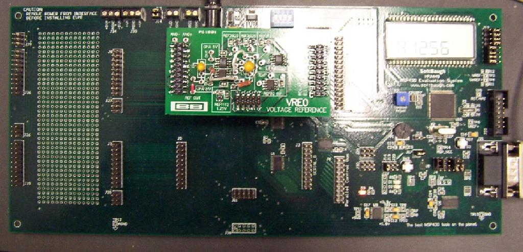
5 Board 5

6 Board (side view) 6
7 Considerations u Low Noise u Long term stability Time Temperature 7
8 Experiment Design R1 C1 OPA R2 C2 RMS noise free bits u u Additional considerations: Vin amplitude, f s (data output rate) 8

9 Confirm the Setup REF R1 C1 OPA R2 C2 RMSnfb k 47u u 23.8 VIn=0V, shorted inputs, 9
10 Results REF R1 C1 OPA R2 C2 RMSnfb OPA u k 220u same same same k 47u same same same same same same same same same same same same same * same same same same same same same OPA227 same same 22.4 Vin=2.5V, data output rate = 60Hz, * OPA in a gain of 2 10
11 Conclusions u On ADS1256 one needs external buffer Input impedance 18k u Noise-wise OPA227 and OPA335 equal However, we tried at T=25 C u REF1004 and REF1112 similar results u REF3xxx family good for lower precision u RC (settling time vs. noise) trade off 11
12 MSP430 u Has 12 bit ADC (ADC12) u Has Vref (2.5V or 1.5V) 800uA max 100ppm/ C max 4% initial accuracy TI REFs: 8uA -110 ua max current ppm/ C 2.048/2.5/3.0V/3.3V 0.2% 12
13 Results REF R1 C1 Noise RMS bits Internal (2.5V) ~ V u ~ k 47u ~ same same ~ same same ~ same ~ same same ~ same same
14 Conclusions Part II u External REFs improve performance Lower noise Lower supply current u REF1112 can not be used with MSP430 VeRef is 1.4V min!!!!! 14
15 Summary u Built tools for evaluations u Got preliminary results u Will work on other ADCs and MSP430 SARs, Delta-Sigma u Will improve datasheets u Support customers with optimal solution Thank You 15


16 Amplifier to A/D Interface Study Or that short task that will not go away Generated by Foxit PDF Creator Foxit Software Bill Klein Senior Applications Engineer Miro Oljaca Strategic Marketing: Motor Control With major contributions from: Tom Hendrick, Tim Green, Rick Downs, Rod Burt, Bob Benjamin, Bernd Rundel, Bruce Trump, Dennis Goeke, Pat Highton 16
17 The Interface Circuit R C sw samp R sw C SH (20pF to 50pF) V int (V cc, 0.5V cc, or GND) sw conv Op Amp Filter A/D CMV Range, V OS vs CMV Charge Bucket Acquisition Time RR Out-Swing to the rail Filtering, Input Circuit Parameters Slew Rate, Signal BW, C load Isolation, Initial Voltage on C SH Load Transient, Settling Time, Output Impedance, 17
18 LSB Size usignal range: +/-10V is a 20V range 12 bits: 20V/4,096 = 4.88mV per LSB 16 bits: 20V/65,536 = 305µV per LSB +5V range 12 bits: 5V/4,096 = 1.22mV per LSB 16 bits: 5V/65,536 = 76.2µV per LSB 24 bits: 5V/16,777,216 = 298nV per LSB +3.3V range 12 bits: 3.3V/4,096 = 806µV per LSB 16 bits: 3.3V/65,536 = 50.4µV per LSB 24 bits: 3.3V/16,777,216 = 196nV per LSB 18
19 Op Amp Input Concerns See Appendix R C sw samp R sw C SH (20pF to 50pF) V int (V cc, 0.5V cc, or GND) sw conv Rail-to-Rail Input 19
20 Output Stage Concerns See Appendix R C sw samp R sw C SH (20pF to 50pF) V int (V cc, 0.5V cc, or GND) sw conv Rail-to-Rail Output 20
21 How Fast does that Op Amp Settle R C sw samp R sw C SH (20pF to 50pF) V int (V cc, 0.5V cc, or GND) sw conv 21
22 What Settling Time? uthink of a linear voltage regulator, there are TWO Settling Times. Line Transient Load Transient usame applies here. udata sheets report settling time to 0.01% at best. 22
23 The Test Circuit C fb REF V-1 +15V-1 OPA227-15V V 2.0K 10K +5V DUT R fil C fil Ref ADS K 10K 2.5V ADS CMD Acquire Convert 30usec T Conv Acq Conv Increment in 20nsec steps 4.0V DUT Out 0.5V 23
24 OPA Bits Series1 Series2 Series3 Series Time (nsec) 24
25 OPA Series1 Series
26 OPA
27 Line Transient Becomes uresponse to change in input signal uincludes Slew Rate. uop Amp data sheets MAY address Settling Time to 0.01% ubut we need % for a 16 bit system 27
28 Required Settling Time Number of bits 0.5LSB % % % % % % % % See appendix for calculations 28
29 Load Transient is UNKNOWN uwe know the load is the input capacitance of the A/D uwe do NOT know the starting voltage. Possible voltages: GND, Mid-Rail, Random Not given in data sheet uthe Op Amp data sheet does NOT even mention this settling time. 29
30 SAR A/D < 500kHz u 70% Applications Slow Moving Real World Process Signals Fast Acquisition & Conversion Allows More System Time For Processing, Computation, Decision Making Multiplexed, Scanning Systems for Slow Moving Signals u 30% Applications AC Fast Moving Dynamic Signals Real Time Processing of Input Signals 30
31 Look at the Charge Transients 31
32 Capacitor Type is Critical R C sw samp R sw C SH (20pF to 50pF) V int (V cc, 0.5V cc, or GND) sw conv 32
33 THD+N vs. Frequency for Various Capacitor types d B k 2k 5k 10k 20k 50k 100k 200k Hz Sweep Trace Color Line Style Thick Data Axis Comment 1 1 Yellow Solid 1 Anlr.THD+N Ratio Left C = Red Solid 1 Anlr.THD+N Ratio Left C1 3 1 Blue Solid 1 Anlr.THD+N Ratio Left C2 4 1 Cyan Solid 1 Anlr.THD+N Ratio Left C3 5 1 Green Solid 1 Anlr.THD+N Ratio Left C4 R = 100 ohm, C = 3.3 nf, Vp-p = 5V f(-3db) = 482 khz 33
34 THD+N vs. Voltage for Various Capacitor Types d B Vrms Sweep Trace Color Line Style Thick Data Axis Comment 1 1 Yellow Solid 1 Anlr.THD+N Ratio Left C = Red Solid 1 Anlr.THD+N Ratio Left C1 3 1 Blue Solid 1 Anlr.THD+N Ratio Left C2 4 1 Cyan Solid 1 Anlr.THD+N Ratio Left C3 5 1 Green Solid 1 Anlr.THD+N Ratio Left C4 R = 100 ohm, C = 3.3 nf, f = 10 khz, f(-3db) = 482 khz 34
35 Conclusions on C Type ubest performance: Sliver Mica or COG(NPO) uavoid all other uothers may cost less and be smaller but can distort signal 35
36 Selecting the Fly-wheel Values R C sw samp R sw C SH (20pF to 50pF) V int (V cc, 0.5V cc, or GND) sw conv 36
37 Fly Wheel Component Selection u Pick C =20*C SH (See Appendix for proof) u R Calculation t _settle = t SAMPL = 12 τ FLT Theoretical Minimum Practical results Use t =18τ FLT Margin for: Op Amp Output Load Transient Op Amp Output Small Signal Settling Time R = t SAMPL /18 C 37
38 ADC Sampling Considerations Voltage on the sampling capacitor during sampling period V C ( t) = V0 + ( E V0 ) (1 e t τ ) 1) E V V t C ( t ) AQ 1 2 LSB 1 ) E (1 2 C ( AQ 17 t AQ τ E V ln( E ) ) 38
39 ADC Sampling Considerations Suggested input sampling switch transient-immunity RC filter R SW R SW V C C C S V 0 τ E ln( t AQ V E ) 39
40 Required Settling Time Number of bits 0.5LSB Time Constants % % % % % % % % 18 See appendix for calculations 40
41 Establish Op Amp Specs Determine Op Amp specs needed based on system values set in design. Op Amp specs to be determined: uugbw uslew Rate ui out 41
42 Impact on UGBW u Modified A ol due to R FLT & C FLT f PX = 1/[2 Π(R O + R FLT )C FLT ] f ZX = 1/[2 Π R FLT C FLT ] u Stability Check At f cl Rate-of-closure is 20dB/decade f ZX cancels f PX before f cl f PX and f ZX are < decade apart Phase of pole will be cancelled by phase of zero This implies: R FLT < 9 R O u Impact on UGBW UGBW mod = UGBW orig -(f ZX - f PX ) 42

43 Impact on UGBW-cont 43
44 Op Amp Specs to Check uugbw mod >2* 1/[2 Π R FLT C FLT ] uop Amp Transient Output Drive to R FLT & C FLT I Opk max = (5% V REF )/(R FLT ) 44
45 Interface Design Check List uop Amp Common Mode Voltage uop Amp Output Swing to Rail uop Amp Settling Time ufilter Capacitor Type ufilter Component Values uop Amp Specifications 45
46 Appendix Calculation Details 1.C as a Function of C sh 2.Open Loop Output Resistance vs. Closed Loop Output Resistance 3.Modified A ol Calculations 4.Time to Charge Capacitor 46
47 Op Amp Input Concerns R C sw samp R sw C SH (20pF to 50pF) V int (V cc, 0.5V cc, or GND) sw conv Rail-to-Rail Input 47
48 Input Stage-Parallel P-ch & N-ch +V SUPPLY V IN - Q 1 Q 2 V IN + Q 3 Q 4 -V SUPPLY 48
49 Looking at Input Stage Performance 1.0kΩ 1.0kΩ kΩ 100kΩ Gain=100 49
50 Single Supply RRI Plot-V OS vs CMV (Most RRI Op Amps Except OPA363/OPA364) OPA2340 (Dual: V OUT1 & V OUT2 from different halves) CMV V OUT1 V OUT2 50
51 Performance Requirements The simple buffer stage. Most accurate unity gain. V IN - + V+ V OUT Bits (mv) (db)

52 OPA350 Data Sheet THD+N 52
53 Possible Input Schemes - V+ V OUT V B - V+ V OUT V IN + (A) Good V IN + (B) Better V IN - V+ V OUT V B + (C) Best 53
54 OPA350 THD+N vs Frequency d B k 2k 5k 10k 20k 50k 100k 200k Hz Sweep Trace Color Line Style Thick Data Axis Comment 1 1 Yellow Solid 1 Anlr.THD+N Ratio Left OPA350 High CMRR G= Red Solid 1 Anlr.THD+N Ratio Left OPA350 High CMRR G= Blue Solid 1 Anlr.THD+N Ratio Left OPA350 Low CMRR G= Cyan Solid 1 Anlr.THD+N Ratio Left OPA350 Low CMRR G=-1 OPA 350, R = 0 ohm, C = 0 nf, Vp-p = 4 V, G = +1or -1 54
55 OPA350 with RC, THD+N vs Frequency d B k 2k 5k 10k 20k 50k 100k 200k Hz Sweep Trace Color Line Style Thick Data Axis Comment 1 1 Yellow Solid 1 Anlr.THD+N Ratio Left OPA350 Low CMRR G=+1 C1 2 1 Red Solid 1 Anlr.THD+N Ratio Left OPA350 Low CMRR G=-1 C4 OPA 350, R = 100 ohm, C = 3.3 nf, Vp-p = 4 V, f(-3db) = 482 khz, G = +1or -1 55
56 OPA350 THD+N vs Input Voltage d B Vpp Sweep Trace Color Line Style Thick Data Axis Comment 1 1 Yellow Solid 1 Anlr.THD+N Ratio Left OPA350 Low CMRR 1kHz 2 1 Red Solid 1 Anlr.THD+N Ratio Left OPA350 Low CMRR 10kHz 3 1 Cyan Solid 1 Anlr.THD+N Ratio Left OPA350 Low CMRR 50kHz 4 1 Green Solid 1 Anlr.THD+N Ratio Left OPA350 Low CMRR 100kHz OPA 350, R = 0 ohm, C = 0 nf, G = -1 56
57 Output Stage Concerns R C sw samp R sw C SH (20pF to 50pF) V int (V cc, 0.5V cc, or GND) sw conv Rail-to-Rail Output 57
58 OPA KHz 10KHz -50 THD+N V(out) 58
59 OPA KHz 10KHz -50 THD+N V(out) 59
60 Solution Circuit - + +In ADS8361 usince Op Amp can only swing 4.8Vp-p uset ADS FSR to 4.8V by reducing Ref in to 2.4V. 2.5V -In Ref Out Ref In 2.4V 60
61 Filter Design Example u R SW = 100Ω (Not needed for Buffer & Filter Calculations) u C SH = 50pF [for ADS8361] u Worst case ΔV across C SH is V REF V REF = +5V u t SAMPL = 1.88μs [for ADS8361] 61
62 Filter Design Example(cont) u Charge Transfer Equation: Q = CV u Charge required to charge C SH to V REF Q SH = C SH V REF Q SH = 50pF 5V = 250pC u IDEAL C FLT Charge Bucket to fill C SH with only a 76μV (1/2LSB) droop on C FLT Q FLT =Q SH Q FLT = C FLT (38μV) 250pC = C FLT (38μV) C FLT = 6.6μF u IDEAL C FLT = 6.6μF Not a good, small, cheap high frequency ceramic capacitor Not practical for Op Amp to drive directly (stability, transient current) Isolation resistor likely not large enough to help isolate Cload and still meet necessary filter time constant 62
63 Filter Design Example(cont) u Partition the Charge Bucket 95% from C FLT 5% from Op Amp u C FLT value required to provide Q SH with <5% droop on C FLT Q FLT = Q SH Q FLT = C FLT (0.05V REF ) 250pC = C FLT (0.05 5V) C FLT = 1nF u During t SAMPL the Op Amp must provide 5% V REF to C FLT Ensure C FLT is at least 10X > C SH This implies dominant load for Op Amp Buffer is C FLT 1nF = 20 X 50pF C FLT = 20X C SH 63
64 Op Amp Model for Derivation of R OUT 64
65 Derivation of R OUT (Closed Loop Output Resistance) β = V FB /V OUT = [V OUT (R I / {R F + R I })]/V OUT = R I / (R F + R I ) R OUT = V OUT /I OUT V O = -V E Aol V E = V OUT [R I /(R F + R I )] V OUT = V O + I OUT R O V OUT = -V E Aol + I OUT R O V OUT = -V OUT [R I /(R F + R I )] Aol+ I OUT R O V OUT + V OUT [R I /(R F + R I )] Aol = I OUT R O V OUT = I OUT R O / {1+[R I Aol/(R F +R I )]} R OUT = V OUT /I OUT = I OUT R O / {1+[R I A OL /(R F +R I )]} R OUT = R O / (1+Aolβ)


66 OPA353 Specifications R O = 40Ω R OUT (@1MHz, G=10) = 10Ω = 29.54dB = x30 66
67 OPA353 R OUT Calculation R O = 40Ω R OUT (@1MHz, G=10) = 10Ω = 29.54dB = x30 67
68 R OUT vs R O u R O does not change when feedback is used to close the loop u Closed loop feedback forces V O to increase/decrease u The increase/decrease in V O appears at V OUT as a reduction in R O u R OUT is the net effect of R O and closed loop feedback controlling V O 68
69 Op Amp Model for AC Stability Analysis R O is constant over the Op Amp s bandwidth R O is defined as the Op Amp s Open Loop Output Resistance R O is measured at I OUT = 0 Amps, f = 1MHz R O is included in β calculation 69
70 Aol Modified by Filter Original Aol f P f Z E E E E E+07 70
71 Modified Aol-The Math V OUT = V R O O R + R 1 + sc 1 + sc V OUT V O = K = 1 R + sc 1 RO + R + sc V OUT V O = K = sc sc + 1 ( R + R ) + 1 O R V OUT V O = K = C ( R + R ) C O s + C R 1 R s + C 1 R 71
72 72 Modified Aol-The Math cont. ( ) ( ) = = O f f O O OUT R R C R C R C s R R C R C R C s K V V 1 1 ( ) ( ) = = O O O OUT R R R R C s R R R R C s K V V 1 1 ( ) ( ) = = O O O OUT R R C s R C s R R R K V V 1 1 ( ) z O p R C f R R C f Π = + Π = 2 1 ; 2 1 Generated by Foxit PDF Creator Foxit Software
73 Voltage on the sampling capacitor during sampling period VC ( t) = V0 + ( E V0 ) (1 e 1 E VC ( taq) LSB 2 V 1 ) E (1 2 C ( t AQ 17 t AQ τ E V ln( E ) ) t τ ) 73
Bipolar Emitter-Follower: Riso w/dual Feedback
 Operational Amplifier Stability Part 10 of 15: Capacitor Loop Stability: Riso with Dual Feedback by Tim Green Linear Applications Engineering Manager, Burr-Brown Products from Texas Instruments Part 10
EE247 Analog-Digital Interface Integrated Circuits
 EE247 Analog-Digital Interface Integrated Circuits Fall 200 Name: Zhaoyi Kang SID: 22074 ******************************************************************************* EE247 Analog-Digital Interface Integrated
Sample-and-Holds David Johns and Ken Martin University of Toronto
 Sample-and-Holds David Johns and Ken Martin (johns@eecg.toronto.edu) (martin@eecg.toronto.edu) slide 1 of 18 Sample-and-Hold Circuits Also called track-and-hold circuits Often needed in A/D converters
Homework Assignment 08
 Homework Assignment 08 Question 1 (Short Takes) Two points each unless otherwise indicated. 1. Give one phrase/sentence that describes the primary advantage of an active load. Answer: Large effective resistance
Switched Capacitor: Sampled Data Systems
 Switched Capacitor: Sampled Data Systems Basic switched capacitor theory How has Anadigm utilised this. Theory-Basic SC and Anadigm-1 Resistor & Charge Relationship I + V - I Resistance is defined in terms
SHM-14 Ultra-Fast, 14-Bit Linear Monolithic Sample-Hold Amplifiers
 INNOVATION and EX C ELL E N C E Ultra-Fast, 1-Bit Linear Monolithic Sample-Hold Amplifiers FEATURES Fast acquisition time: 10ns to ±0.1% 0ns to ±0.0% ns to ±0.01% ±0.001% Nonlinearity 6µV rms output noise
Final Exam. 55:041 Electronic Circuits. The University of Iowa. Fall 2013.
 Final Exam Name: Max: 130 Points Question 1 In the circuit shown, the op-amp is ideal, except for an input bias current I b = 1 na. Further, R F = 10K, R 1 = 100 Ω and C = 1 μf. The switch is opened at
Homework Assignment 11
 Homework Assignment Question State and then explain in 2 3 sentences, the advantage of switched capacitor filters compared to continuous-time active filters. (3 points) Continuous time filters use resistors
EXAMPLE DESIGN PART 2
 ECE37 Advanced Analog Circuits Lecture 4 EXAMPLE DESIGN PART 2 Richard Schreier richard.schreier@analog.com Trevor Caldwell trevor.caldwell@utoronto.ca Course Goals Deepen understanding of CMOS analog
Switched-Capacitor Circuits David Johns and Ken Martin University of Toronto
 Switched-Capacitor Circuits David Johns and Ken Martin University of Toronto (johns@eecg.toronto.edu) (martin@eecg.toronto.edu) University of Toronto 1 of 60 Basic Building Blocks Opamps Ideal opamps usually
DESIGN MICROELECTRONICS ELCT 703 (W17) LECTURE 3: OP-AMP CMOS CIRCUIT. Dr. Eman Azab Assistant Professor Office: C
 LECTURE 3: OP-AMP CMOS CIRCUIT. Dr. Eman Azab Assistant Professor Office: C") MICROELECTRONICS ELCT 703 (W17) LECTURE 3: OP-AMP CMOS CIRCUIT DESIGN Dr. Eman Azab Assistant Professor Office: C3.315 E-mail: eman.azab@guc.edu.eg 1 TWO STAGE CMOS OP-AMP It consists of two stages: First
MICROELECTRONICS ELCT 703 (W17) LECTURE 3: OP-AMP CMOS CIRCUIT DESIGN Dr. Eman Azab Assistant Professor Office: C3.315 E-mail: eman.azab@guc.edu.eg 1 TWO STAGE CMOS OP-AMP It consists of two stages: First
E40M. Op Amps. M. Horowitz, J. Plummer, R. Howe 1
 E40M Op Amps M. Horowitz, J. Plummer, R. Howe 1 Reading A&L: Chapter 15, pp. 863-866. Reader, Chapter 8 Noninverting Amp http://www.electronics-tutorials.ws/opamp/opamp_3.html Inverting Amp http://www.electronics-tutorials.ws/opamp/opamp_2.html
Chapter 10 Feedback. PART C: Stability and Compensation
 1 Chapter 10 Feedback PART C: Stability and Compensation Example: Non-inverting Amplifier We are analyzing the two circuits (nmos diff pair or pmos diff pair) to realize this symbol: either of the circuits
Operational Amplifiers
 Operational Amplifiers A Linear IC circuit Operational Amplifier (op-amp) An op-amp is a high-gain amplifier that has high input impedance and low output impedance. An ideal op-amp has infinite gain and
ELECTRONIC SYSTEMS. Basic operational amplifier circuits. Electronic Systems - C3 13/05/ DDC Storey 1
 Electronic Systems C3 3/05/2009 Politecnico di Torino ICT school Lesson C3 ELECTONIC SYSTEMS C OPEATIONAL AMPLIFIES C.3 Op Amp circuits» Application examples» Analysis of amplifier circuits» Single and
Maxim Integrated Products 1
 19-4187; Rev 4; 7/1 μ μ PART AMPS PER PACKAGE PIN- PACKAGE + * TOP MARK MAX965AZK+ 1 5 SOT3 ADSI MAX965AZK/V+ 1 5 SOT3 ADSK MAX965AUA+ 1 8 μmax-ep* AABI MAX965ATA+ 1 8 TDFN-EP* BKX MAX9651AUA+ 8 μmax-ep*
Advanced Current Mirrors and Opamps
 Advanced Current Mirrors and Opamps David Johns and Ken Martin (johns@eecg.toronto.edu) (martin@eecg.toronto.edu) slide 1 of 26 Wide-Swing Current Mirrors I bias I V I in out out = I in V W L bias ------------
Lecture 10, ATIK. Data converters 3
 Lecture, ATIK Data converters 3 What did we do last time? A quick glance at sigma-delta modulators Understanding how the noise is shaped to higher frequencies DACs A case study of the current-steering
Time Varying Circuit Analysis
 MAS.836 Sensor Systems for Interactive Environments th Distributed: Tuesday February 16, 2010 Due: Tuesday February 23, 2010 Problem Set # 2 Time Varying Circuit Analysis The purpose of this problem set
Precision, Micropower, Low-Dropout, High- Output-Current, SO-8 Voltage References
 19-165; Rev ; 7/ Precision, Micropower, Low-Dropout, High- General Description The MAX6167 are precision, low-dropout, micropower voltage references. These three-terminal devices operate with an input
UNIVERSITÀ DEGLI STUDI DI CATANIA. Dottorato di Ricerca in Ingegneria Elettronica, Automatica e del Controllo di Sistemi Complessi, XXII ciclo
 UNIVERSITÀ DEGLI STUDI DI CATANIA DIPARTIMENTO DI INGEGNERIA ELETTRICA, ELETTRONICA E DEI SISTEMI Dottorato di Ricerca in Ingegneria Elettronica, Automatica e del Controllo di Sistemi Complessi, XXII ciclo
Systematic Design of Operational Amplifiers
 Systematic Design of Operational Amplifiers Willy Sansen KULeuven, ESAT-MICAS Leuven, Belgium willy.sansen@esat.kuleuven.be Willy Sansen 10-05 061 Table of contents Design of Single-stage OTA Design of
Fig. 2.0: SPICE Loop Gain Test
 Operational Amplifier Stability Part 2 of 15: Op Amp Networks, SPICE Analysis by Tim Green Strategic Development Engineer, BurrBrown Products from Texas Instruments Incorporated Part 2 of this series focuses
Monolithic N-Channel JFET Dual
 N9 Monolithic N-Channel JFET Dual V GS(off) (V) V (BR)GSS Min (V) g fs Min (ms) I G Max (pa) V GS V GS Max (mv). to. Monolithic Design High Slew Rate Low Offset/Drift Voltage Low Gate Leakage: pa Low Noise:
OPERATIONAL AMPLIFIER APPLICATIONS
 OPERATIONAL AMPLIFIER APPLICATIONS 2.1 The Ideal Op Amp (Chapter 2.1) Amplifier Applications 2.2 The Inverting Configuration (Chapter 2.2) 2.3 The Non-inverting Configuration (Chapter 2.3) 2.4 Difference
D/A Converters. D/A Examples
 D/A architecture examples Unit element Binary weighted Static performance Component matching Architectures Unit element Binary weighted Segmented Dynamic element matching Dynamic performance Glitches Reconstruction
EECE 2150 Circuits and Signals, Biomedical Applications Final Exam Section 3
 EECE 2150 Circuits and Signals, Biomedical Applications Final Exam Section 3 Instructions: Closed book, closed notes; Computers and cell phones are not allowed You may use the equation sheet provided but
Lecture 340 Characterization of DACs and Current Scaling DACs (5/1/10) Page 340-1
 Page 340-1") Lecture 34 Characterization of DACs and Current Scaling DACs (5//) Page 34 LECTURE 34 CHARACTERZATON OF DACS AND CURRENT SCALNG DACS LECTURE ORGANZATON Outline ntroduction Static characterization of DACs
Lecture 34 Characterization of DACs and Current Scaling DACs (5//) Page 34 LECTURE 34 CHARACTERZATON OF DACS AND CURRENT SCALNG DACS LECTURE ORGANZATON Outline ntroduction Static characterization of DACs
Lecture 4: Feedback and Op-Amps
 Lecture 4: Feedback and Op-Amps Last time, we discussed using transistors in small-signal amplifiers If we want a large signal, we d need to chain several of these small amplifiers together There s a problem,
Georgia Institute of Technology School of Electrical and Computer Engineering. Midterm-1 Exam (Solution)
") Georgia Institute of Technology School of Electrical and Computer Engineering Midterm-1 Exam (Solution) ECE-6414 Spring 2012 Friday, Feb. 17, 2012 Duration: 50min First name Solutions Last name Solutions
Georgia Institute of Technology School of Electrical and Computer Engineering Midterm-1 Exam (Solution) ECE-6414 Spring 2012 Friday, Feb. 17, 2012 Duration: 50min First name Solutions Last name Solutions
Monolithic N-Channel JFET Duals
 Monolithic N-Channel JFET Duals N96/97/98/99 Part Number V GS(off) (V) V (BR)GSS Min (V) Min (ms) I G Max (pa) V GS V GS Max (mv) N96.7 to N97.7 to N98.7 to N99.7 to Monolithic Design High Slew Rate Low
System on a Chip. Prof. Dr. Michael Kraft
 System on a Chip Prof. Dr. Michael Kraft Lecture 3: Sample and Hold Circuits Switched Capacitor Circuits Circuits and Systems Sampling Signal Processing Sample and Hold Analogue Circuits Switched Capacitor
D is the voltage difference = (V + - V - ).
.") 1 Operational amplifier is one of the most common electronic building blocks used by engineers. It has two input terminals: V + and V -, and one output terminal Y. It provides a gain A, which is usually
1 Operational amplifier is one of the most common electronic building blocks used by engineers. It has two input terminals: V + and V -, and one output terminal Y. It provides a gain A, which is usually
CE/CS Amplifier Response at High Frequencies
 .. CE/CS Amplifier Response at High Frequencies INEL 4202 - Manuel Toledo August 20, 2012 INEL 4202 - Manuel Toledo CE/CS High Frequency Analysis 1/ 24 Outline.1 High Frequency Models.2 Simplified Method.3
Electronic Circuits. Prof. Dr. Qiuting Huang Integrated Systems Laboratory
 Electronic Circuits Prof. Dr. Qiuting Huang 6. Transimpedance Amplifiers, Voltage Regulators, Logarithmic Amplifiers, Anti-Logarithmic Amplifiers Transimpedance Amplifiers Sensing an input current ii in
KH600. 1GHz, Differential Input/Output Amplifier. Features. Description. Applications. Typical Application
 KH 1GHz, Differential Input/Output Amplifier www.cadeka.com Features DC - 1GHz bandwidth Fixed 1dB (V/V) gain 1Ω (differential) inputs and outputs -7/-dBc nd/3rd HD at MHz ma output current 9V pp into
EXAMPLE DESIGN PART 2
 ECE37 Advanced Analog Circuits Lecture 3 EXAMPLE DESIGN PART 2 Richard Schreier richard.schreier@analog.com Trevor Caldwell trevor.caldwell@utoronto.ca Course Goals Deepen understanding of CMOS analog
Application Report. Mixed Signal Products SLOA021
 Application Report May 1999 Mixed Signal Products SLOA021 IMPORTANT NOTICE Texas Instruments and its subsidiaries (TI) reserve the right to make changes to their products or to discontinue any product
LASER PULSE DETECTION: The Tradeoff between Pulse Resolution and Responsivity
 ELTECdata #134 LASER PULSE DETECTION: The Tradeoff between Pulse Resolution and Responsivity ELTEC INSTRUMENTS, INC. I. VOLTAGE MODE APPROACH C R Output Pyroelectric Crystal "Self-Generating" Capacitor
SGM nA, Non-Unity Gain, Dual Rail-to-Rail Input/Output Operational Amplifier
 PRODUCT DESCRIPTION The SGM8046 operates with a single supply voltage as low as 1.4V, while drawing less than 670nA (TYP) of quiescent current per amplifier. This device is also designed to support rail-to-rail
Lab #4 Capacitors and Inductors. Capacitor Transient and Steady State Response
 Capacitor Transient and Steady State Response Like resistors, capacitors are also basic circuit elements. Capacitors come in a seemingly endless variety of shapes and sizes, and they can all be represented
Design Engineering MEng EXAMINATIONS 2016
 IMPERIAL COLLEGE LONDON Design Engineering MEng EXAMINATIONS 2016 For Internal Students of the Imperial College of Science, Technology and Medicine This paper is also taken for the relevant examination
H(s) = 2(s+10)(s+100) (s+1)(s+1000)
 = 2(s+10)(s+100) (s+1)(s+1000)") Problem 1 Consider the following transfer function H(s) = 2(s10)(s100) (s1)(s1000) (a) Draw the asymptotic magnitude Bode plot for H(s). Solution: The transfer function is not in standard form to sketch
Problem 1 Consider the following transfer function H(s) = 2(s10)(s100) (s1)(s1000) (a) Draw the asymptotic magnitude Bode plot for H(s). Solution: The transfer function is not in standard form to sketch
Low-Sensitivity, Highpass Filter Design with Parasitic Compensation
 Low-Sensitivity, Highpass Filter Design with Parasitic Compensation Introduction This Application Note covers the design of a Sallen-Key highpass biquad. This design gives low component and op amp sensitivities.
NCS1002A. Constant Voltage / Constant Current Secondary Side Controller
 NCS00A Constant Voltage / Constant Current Secondary Side Controller Description The NCS00A is a performance upgrade from the NCS00 focused on reducing power consumption in applications that require more
EMC Considerations for DC Power Design
 EMC Considerations for DC Power Design Tzong-Lin Wu, Ph.D. Department of Electrical Engineering National Sun Yat-sen University Power Bus Noise below 5MHz 1 Power Bus Noise below 5MHz (Solution) Add Bulk
ESE319 Introduction to Microelectronics. Feedback Basics
 Feedback Basics Stability Feedback concept Feedback in emitter follower One-pole feedback and root locus Frequency dependent feedback and root locus Gain and phase margins Conditions for closed loop stability
Guest Lectures for Dr. MacFarlane s EE3350
 Guest Lectures for Dr. MacFarlane s EE3350 Michael Plante Sat., -08-008 Write name in corner.. Problem Statement Amplifier Z S Z O V S Z I Z L Transducer, Antenna, etc. Coarse Tuning (optional) Amplifier
MAX14753 V DD INA0 INA1 INA2 INA3 OUT INB0 INB1 INB2 INB3
 19-4255; Rev 3; 7/10 8-Channel/Dual 4-Channel General Description The are 8-to-1 and dual 4-to-1 high-voltage analog multiplexers. Both devices feature 60Ω (typ) on-resistance with 0.03Ω (typ) on-resistance
High-Supply-Voltage, Precision Voltage Reference in SOT23 MAX6035
 19-2606; Rev 3; 11/06 High-Supply-Voltage, Precision General Description The is a high-voltage, precision micropower voltage reference. This three-terminal device is available with output voltage options
SGM nA, Non-Unity Gain, Quad Rail-to-Rail Input/Output Operational Amplifier
 PRODUCT DESCRIPTION The SGM8048 operates with a single supply voltage as low as 1.4V, while drawing less than 690nA (TYP) of quiescent current per amplifier. This device is also designed to support rail-to-rail
ECEN 610 Mixed-Signal Interfaces
 ECEN 610 Mixed-Signal Interfaces Sebastian Hoyos Texas A&M University Analog and Mixed Signal Group Spring 014 S. Hoyos-ECEN-610 1 Sample-and-Hold Spring 014 S. Hoyos-ECEN-610 ZOH vs. Track-and-Hold V(t)
SC70, 1.6V, Nanopower, Beyond-the-Rails Comparators With/Without Reference
 19-1862; Rev 4; 1/7 SC7, 1.6V, Nanopower, Beyond-the-Rails General Description The nanopower comparators in space-saving SC7 packages feature Beyond-the- Rails inputs and are guaranteed to operate down
Electronic Circuits Summary
 Electronic Circuits Summary Andreas Biri, D-ITET 6.06.4 Constants (@300K) ε 0 = 8.854 0 F m m 0 = 9. 0 3 kg k =.38 0 3 J K = 8.67 0 5 ev/k kt q = 0.059 V, q kt = 38.6, kt = 5.9 mev V Small Signal Equivalent
EXAMPLE DESIGN PART 1
 ECE37 Advanced Analog Circuits Lecture 3 EXAMPLE DESIGN PART Richard Schreier richard.schreier@analog.com Trevor Caldwell trevor.caldwell@utoronto.ca Course Goals Deepen understanding of CMOS analog circuit
Lecture 6, ATIK. Switched-capacitor circuits 2 S/H, Some nonideal effects Continuous-time filters
 Lecture 6, ATIK Switched-capacitor circuits 2 S/H, Some nonideal effects Continuous-time filters What did we do last time? Switched capacitor circuits The basics Charge-redistribution analysis Nonidealties
Lecture 37: Frequency response. Context
 EECS 05 Spring 004, Lecture 37 Lecture 37: Frequency response Prof J. S. Smith EECS 05 Spring 004, Lecture 37 Context We will figure out more of the design parameters for the amplifier we looked at in
General Purpose Transistors
 General Purpose Transistors NPN and PNP Silicon These transistors are designed for general purpose amplifier applications. They are housed in the SOT 33/SC which is designed for low power surface mount
2N5545/46/47/JANTX/JANTXV
 N//7/JANTX/JANTXV Monolithic N-Channel JFET Duals Product Summary Part Number V GS(off) (V) V (BR)GSS Min (V) g fs Min (ms) I G Max (pa) V GS V GS Max (mv) N. to.. N. to.. N7. to.. Features Benefits Applications
Homework Assignment 09
 Homework Assignment 09 Question 1 (Short Takes) Two points each unless otherwise indicated. 1. What is the 3-dB bandwidth of the amplifier shown below if r π = 2.5K, r o = 100K, g m = 40 ms, and C L =
55:041 Electronic Circuits The University of Iowa Fall Final Exam
 Final Exam Name: Score Max: 135 Question 1 (1 point unless otherwise noted) a. What is the maximum theoretical efficiency for a class-b amplifier? Answer: 78% b. The abbreviation/term ESR is often encountered
ENGN3227 Analogue Electronics. Problem Sets V1.0. Dr. Salman Durrani
 ENGN3227 Analogue Electronics Problem Sets V1.0 Dr. Salman Durrani November 2006 Copyright c 2006 by Salman Durrani. Problem Set List 1. Op-amp Circuits 2. Differential Amplifiers 3. Comparator Circuits
1/13/12 V DS. I d V GS. C ox ( = f (V GS ,V DS ,V SB = I D. + i d + I ΔV + I ΔV BS V BS. 19 January 2012
 /3/ 9 January 0 Study the linear model of MOS transistor around an operating point." MOS in saturation: V GS >V th and V S >V GS -V th " VGS vi - I d = I i d VS I d = µ n ( L V V γ Φ V Φ GS th0 F SB F
SGM nA, Dual Rail-to-Rail I/O Operational Amplifier
 SGM842 67nA, Dual Rail-to-Rail I/O GENERAL DESCRIPTION The SGM842 is guaranteed to operate with a single supply voltage as low as 1.4V, while drawing less than 67nA (TYP) of quiescent current per amplifier.
Section 4. Nonlinear Circuits
 Section 4 Nonlinear Circuits 1 ) Voltage Comparators V P < V N : V o = V ol V P > V N : V o = V oh One bit A/D converter, Practical gain : 10 3 10 6 V OH and V OL should be far apart enough Response Time:
Low Drift, Low Power Instrumentation Amplifier AD621
 a FEATURES EASY TO USE Pin-Strappable Gains of 0 and 00 All Errors Specified for Total System Performance Higher Performance than Discrete In Amp Designs Available in -Lead DIP and SOIC Low Power,.3 ma
Pipelined multi step A/D converters
 Department of Electrical Engineering Indian Institute of Technology, Madras Chennai, 600036, India 04 Nov 2006 Motivation for multi step A/D conversion Flash converters: Area and power consumption increase
Lecture 310 Open-Loop Comparators (3/28/10) Page 310-1
 Page 310-1") Lecture 310 Open-Loop Comparators (3/28/10) Page 310-1 LECTURE 310 OPEN-LOOP COMPARATORS LECTURE ORGANIZATION Outline Characterization of comparators Dominant pole, open-loop comparators Two-pole, open-loop
Lecture 310 Open-Loop Comparators (3/28/10) Page 310-1 LECTURE 310 OPEN-LOOP COMPARATORS LECTURE ORGANIZATION Outline Characterization of comparators Dominant pole, open-loop comparators Two-pole, open-loop
Stability and Frequency Compensation
 類比電路設計 (3349) - 2004 Stability and Frequency ompensation hing-yuan Yang National hung-hsing University Department of Electrical Engineering Overview Reading B Razavi hapter 0 Introduction In this lecture,
UNIVERSITY OF CALIFORNIA College of Engineering Department of Electrical Engineering and Computer Sciences
 UNIVERSITY OF CALIFORNIA College of Engineering Department of Electrical Engineering and Computer Sciences E. Alon Final EECS 240 Monday, May 19, 2008 SPRING 2008 You should write your results on the exam
Summary Last Lecture
 EE247 Lecture 19 ADC Converters Sampling (continued) Sampling switch charge injection & clock feedthrough Complementary switch Use of dummy device Bottom-plate switching Track & hold T/H circuits T/H combined
Quick Review. ESE319 Introduction to Microelectronics. and Q1 = Q2, what is the value of V O-dm. If R C1 = R C2. s.t. R C1. Let Q1 = Q2 and R C1
 Quick Review If R C1 = R C2 and Q1 = Q2, what is the value of V O-dm? Let Q1 = Q2 and R C1 R C2 s.t. R C1 > R C2, express R C1 & R C2 in terms R C and ΔR C. If V O-dm is the differential output offset
LM108/LM108AQML Operational Amplifiers
 LM108/LM108AQML Operational Amplifiers General Description The LM108 is a precision operational amplifier having specifications a factor of ten better than FET amplifiers over a 55 C to +125 C temperature
ECE 304: Design Issues for Voltage Follower as Output Stage S&S Chapter 14, pp
 ECE 34: Design Issues for oltage Follower as Output Stage S&S Chapter 14, pp. 131133 Introduction The voltage follower provides a good buffer between a differential amplifier and a load in two ways: 1.
Figure Circuit for Question 1. Figure Circuit for Question 2
 Exercises 10.7 Exercises Multiple Choice 1. For the circuit of Figure 10.44 the time constant is A. 0.5 ms 71.43 µs 2, 000 s D. 0.2 ms 4 Ω 2 Ω 12 Ω 1 mh 12u 0 () t V Figure 10.44. Circuit for Question
LD A high PSRR ultra low drop linear regulator with reverse current protection. Datasheet. Features. Applications.
 Datasheet 2 A high PSRR ultra low drop linear regulator with reverse current protection Features Input voltage from 1.25 V to 6. V Ultra low drop: 13 mv (typ.) at 2 A load 1 % output accuracy at 25 C,
Microelectronic Circuit Design 4th Edition Errata - Updated 4/4/14
 Chapter Text # Inside back cover: Triode region equation should not be squared! i D = K n v GS "V TN " v & DS % ( v DS $ 2 ' Page 49, first exercise, second answer: -1.35 x 10 6 cm/s Page 58, last exercise,
PT5108. High-PSRR 500mA LDO GENERAL DESCRIPTION FEATURES APPLICATIONS TYPICAL APPLICATIONS. Ripple Rejection vs Frequency. Ripple Rejection (db)
") GENERAL DESCRIPTION The PT5108 is a low-dropout voltage regulator designed for portable applications that require both low noise performance and board space. Its PSRR at 1kHz is better than 70dB. The PT5108
GENERAL DESCRIPTION The PT5108 is a low-dropout voltage regulator designed for portable applications that require both low noise performance and board space. Its PSRR at 1kHz is better than 70dB. The PT5108
Lecture 4, Noise. Noise and distortion
 Lecture 4, Noise Noise and distortion What did we do last time? Operational amplifiers Circuit-level aspects Simulation aspects Some terminology Some practical concerns Limited current Limited bandwidth
Bandwidth of op amps. R 1 R 2 1 k! 250 k!
 Bandwidth of op amps An experiment - connect a simple non-inverting op amp and measure the frequency response. From the ideal op amp model, we expect the amp to work at any frequency. Is that what happens?
Errata of CMOS Analog Circuit Design 2 nd Edition By Phillip E. Allen and Douglas R. Holberg
 Errata 2 nd Ed. (5/22/2) Page Errata of CMOS Analog Circuit Design 2 nd Edition By Phillip E. Allen and Douglas R. Holberg Page Errata 82 Line 4 after figure 3.2-3, CISW CJSW 88 Line between Eqs. (3.3-2)
Switched-Capacitor Filters
 Switched-Capacitor Filters Analog sampled-data filters: Continuous amplitude Quantized time Applications: Oversampled and D/A converters Analog front-ends (CDS, etc) Standalone filters E.g. National Semiconductor
DAC10* PRODUCT PAGE QUICK LINKS Last Content Update: 02/23/2017
 * PRODUCT PAGE QUICK LINKS Last Content Update: 0/3/07 COMPARABLE PARTS View a parametric search of comparable parts. DOCUMENTATION Data Sheet : 0-Bit Current-Out DAC Data Sheet REFERENCE MATERIALS Solutions
SGM nA, Single Rail-to-Rail I/O Operational Amplifier
 GENERAL DESCRIPTION The SGM8041 is guaranteed to operate with a single supply voltage as low as 1.4V, while drawing less than 710nA (TYP) of quiescent current. This device is also designed to support rail-to-rail
EXAMPLE DESIGN PART 1
 EE37 Advanced Analog ircuits Lecture 3 EXAMPLE DESIGN PART Richard Schreier richard.schreier@analog.com Trevor aldwell trevor.caldwell@utoronto.ca ourse Goals Deepen understanding of MOS analog circuit
Current feedback operational amplifiers as fast charge sensitive preamplifiers for
 Home Search Collections Journals About Contact us My IOPscience Current feedback operational amplifiers as fast charge sensitive preamplifiers for photomultiplier read out This article has been downloaded
ENGR-4300 Spring 2009 Test 2. Name: SOLUTION. Section: 1(MR 8:00) 2(TF 2:00) 3(MR 6:00) (circle one) Question I (20 points): Question II (20 points):
 2(TF 2:00) 3(MR 6:00) (circle one) Question I (20 points): Question II (20 points):") ENGR43 Test 2 Spring 29 ENGR43 Spring 29 Test 2 Name: SOLUTION Section: 1(MR 8:) 2(TF 2:) 3(MR 6:) (circle one) Question I (2 points): Question II (2 points): Question III (17 points): Question IV (2 points):
ENGR43 Test 2 Spring 29 ENGR43 Spring 29 Test 2 Name: SOLUTION Section: 1(MR 8:) 2(TF 2:) 3(MR 6:) (circle one) Question I (2 points): Question II (2 points): Question III (17 points): Question IV (2 points):
( s) N( s) ( ) The transfer function will take the form. = s = 2. giving ωo = sqrt(1/lc) = 1E7 [rad/s] ω 01 := R 1. α 1 2 L 1.
![( s) N( s) ( ) The transfer function will take the form. = s = 2. giving ωo = sqrt(1/lc) = 1E7 [rad/s] ω 01 := R 1. α 1 2 L 1.](/thumbs/83/87520964.jpg "( s) N( s) ( ) The transfer function will take the form. = s = 2. giving ωo = sqrt(1/lc) = 1E7 [rad/s] ω 01 := R 1. α 1 2 L 1.") Problem ) RLC Parallel Circuit R L C E-4 E-0 V a. What is the resonant frequency of the circuit? The transfer function will take the form N ( ) ( s) N( s) H s R s + α s + ω s + s + o L LC giving ωo sqrt(/lc)
Problem ) RLC Parallel Circuit R L C E-4 E-0 V a. What is the resonant frequency of the circuit? The transfer function will take the form N ( ) ( s) N( s) H s R s + α s + ω s + s + o L LC giving ωo sqrt(/lc)
Ultra-Low-Power Series Voltage Reference
 19-257; Rev 2; 3/5 Ultra-Low-Power Series Voltage Reference General Description The micropower, low-dropout bandgap voltage reference combines ultra-low supply current and low drift in a miniature 5-pin
Ω μ. PKG CODE M AX 5128E LA+ -40 C to +85 C 8 μdfn AAF L822-1 TEMP RANGE PIN - PA C K A G E TOP MARK PART. Maxim Integrated Products 1
 19-3929; Rev 2; 6/7 μ Ω μ μ μ Ω μ PART TEMP RANGE PIN - PA C K A G E TOP MARK PKG M AX 5128E A+ -4 C to +85 C 8 μdfn AAF 822-1 H V CC GND POR 7 7-BIT NV MEMORY 128-POSITION DER 128 TAPS W UP DN SERIA INTERFACE
Cast of Characters. Some Symbols, Functions, and Variables Used in the Book
 Page 1 of 6 Cast of Characters Some s, Functions, and Variables Used in the Book Digital Signal Processing and the Microcontroller by Dale Grover and John R. Deller ISBN 0-13-081348-6 Prentice Hall, 1998
EE247 Lecture 16. Serial Charge Redistribution DAC
 EE47 Lecture 16 D/A Converters D/A examples Serial charge redistribution DAC Practical aspects of current-switch DACs Segmented current-switch DACs DAC self calibration techniques Current copiers Dynamic
AN019. A Better Approach of Dealing with Ripple Noise of LDO. Introduction. The influence of inductor effect over LDO
 Better pproach of Dealing with ipple Noise of Introduction It has been a trend that cellular phones, audio systems, cordless phones and portable appliances have a requirement for low noise power supplies.
RP mA, Ultra-Low Noise, Ultra-Fast CMOS LDO Regulator. General Description. Features. Applications. Ordering Information. Marking Information
 RP122 3mA, Ultra-Low Noise, Ultra-Fast CMOS LDO Regulator General Description The RP122 is designed for portable RF and wireless applications with demanding performance and space requirements. The RP122
Ultra-Low-Power Precision Series Voltage Reference MAX6029. Features. General Description. Ordering Information. Applications.
 MAX629 General Description The MAX629 micropower, low-dropout bandgap voltage reference combines ultra-low supply current and low drift in a miniature 5-pin SOT23 surface-mount package that uses 7% less
SERIALLY PROGRAMMABLE CLOCK SOURCE. Features
 DATASHEET ICS307-03 Description The ICS307-03 is a dynamic, serially programmable clock source which is flexible and takes up minimal board space. Output frequencies are programmed via a 3-wire SPI port.
Frequency Dependent Aspects of Op-amps
 Frequency Dependent Aspects of Op-amps Frequency dependent feedback circuits The arguments that lead to expressions describing the circuit gain of inverting and non-inverting amplifier circuits with resistive
Laboratory III: Operational Amplifiers
 Physics 33, Fall 2008 Lab III - Handout Laboratory III: Operational Amplifiers Introduction Operational amplifiers are one of the most useful building blocks of analog electronics. Ideally, an op amp would
ADC Bit, 50MHz Video A/D Converter
 ADC- -Bit, 0MHz Video A/D Converter FEATURES Low power dissipation (0mW max.) Input signal bandwith (00MHz) Optional synchronized clamp function Low input capacitance (pf typ.) +V or +V /+.V power supply
Experiment Guide for RC Circuits
 Guide-P1 Experiment Guide for RC Circuits I. Introduction 1. Capacitors A capacitor is a passive electronic component that stores energy in the form of an electrostatic field. The unit of capacitance is