FPGA Resource Utilization Estimates for NI PXI-7854R. LabVIEW FPGA Version: 8.6 NI-RIO Version: 3.0 Date: 8/5/2008
|
|
|
- Priscilla Fox
- 6 years ago
- Views:
Transcription
1 FPGA Resource Utilization Estimates for NI PXI-7854R LabVIEW FPGA Version: 8.6 NI-RIO Version: 3.0 Date: 8/5/2008 Note: The numbers presented in this document are estimates. Actual resource usage for your designs may be different (smaller or greater) than the resource usage computed using the information contained in this document. 1. How to use the table An example Resource utilization tables for the functions on the FPGA palette Structures Array Cluster & Variant Numeric Boolean Comparison Timing Memory & FIFO Memory FIFO FIFO DMA host-to-target FIFO DMA target-to-host FPGA Math & Analysis Look-up Table 1D Butterworth filter Notch filter DC & RMS Measurements Fast Fourier Transform Rational Resampler Synchronization Advanced... 29
2 1. How to use the table The tables in this spreadsheet contain approximations of resource usage. To obtain an estimate for your design, add the corresponding numbers for each function/vi you use. Some of the functions on the LabVIEW FPGA palette consume no logic resources on the FPGA because they are purely wiring operations: For more FPGA-specific information about the objects on the palette see LabVIEW Help: VI and Function Reference > FPGA Module VIs and > FPGA VI and Function details. For information on the resources available for the PXI-7854R target, go to: Start menu > Programs > National Instruments > NI-RIO > R Series Intelligent DAQ Specifications Then, look under the heading Reconfigurable FPGA. To allow for target overhead, you should add the following base numbers to the sum of flip flops and the sum of LUTs: Flip LUTs Also add the corresponding numbers for the controls and indicators in your VI(s): Data type Resource usage Flip LUTs Numeric controls and indicators U U U U I I I I FXP<±,8,4> FXP<±,16,8> FXP<±,32,16> FXP<±,64,32>
3 Boolean controls and indicators Boolean 3 4 Data type Fixed array size Resource usage Flip LUTs Array controls and indicators U U U U I I I I FXP<±,8,4> FXP<±,16,8> FXP<±,32,16> FXP<±,64,32> Boolean

4 An example To illustrate the difference between actual resource usage and the estimate obtained using the spreadsheet, we use an example from the NI Example Finder, Counters R Series.lvproj
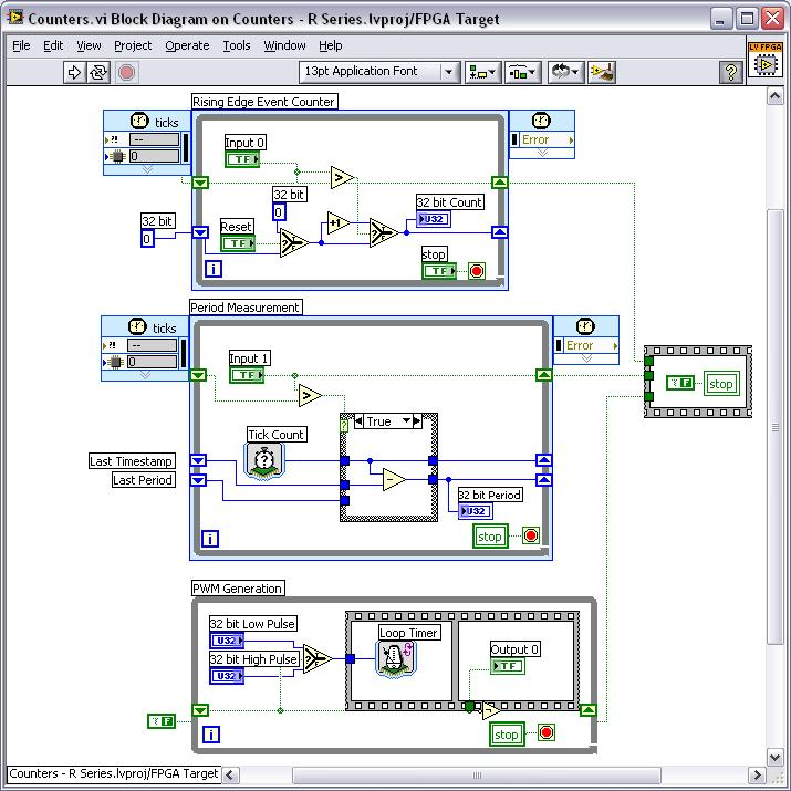
5
6 Actual resource usage: Slice Logic Utilization: Slice Registers: 1,053 out of 69,120 1% Number used as Flip : 1,053 Slice LUTs: 1,070 out of 69,120 1% Number used as logic: 1,061 out of 69,120 1% Number using O6 output only: 906 Number using O5 output only: 76 Number using O5 and O6: 79 Number used as Memory: 6 out of 17,920 1% Number used as Shift Register: 6 Number using O6 output only: 6 Number used as exclusive route-thru: 3 Estimated resource usage: Name of VI/Element Resource Usage Flip LUTs Select I32/U32 SCTL Select I32/U32 SCTL Select I32/U32 SCTL Greater? Boolean SCTL Greater? Boolean SCTL Not SCTL 0 1 Increment I32/U32 SCTL 0 32 Subtract I32/U32 SCTL 0 33 Tick count 32-bit SCTL Loop timer 32-bit Structures Timed Loop Timed Loop Case structure SCTL 0 0 Flat sequence SCTL 0 0 While loop, i terminal unwired Stacked sequence 0 0 Controls and indicators 7x Boolean x U Base Total
7 3. Resource utilization tables for the functions on the FPGA palette 3.1. Structures Name of VI/Element Data Outside SCTL Inside SCTL Type Flip LUTs Flip LUTs Structures For Loop, i terminal wired Not supported For Loop, i terminal unwired Not supported While Loop, i terminal wired 2 3 Not supported While Loop, i terminal unwired Not supported Timed Structures 0 0 Timed Loop Not supported FPGA Clk Const Case Structure Flat Sequence Structure 0 0 No sequencing effect Stacked Sequence Structure 0 0 No sequencing effect Diagram Disable Structure Conditional Disable Structure Local Variable Boolean I8/U I16/U I32/U I64/U Decorations Free Label Thin Line Thin Line with Arrow Flat Frame Thick Line Thick Line with Arrow Feedback Node Boolean I8/U I16/U I32/U I64/U
8 3.2. Array Name of VI/Element Data Array Outside SCTL Inside SCTL Type Size Flip LUTs Flip LUTs Array Array Size Index Array I32/U Replace Array Subset I32/U Insert Into Array Delete From Array Initialize Array Build Array Array Subset Rotate 1D Array I32/U Not supported Reverse 1D Array Split 1D Array Interleave 1D Arrays Decimate 1D Array Array Constant Array to Cluster Cluster to Array Reshape Array
9 3.3. Cluster & Variant Name of VI/Element Outside SCTL Inside SCTL Flip LUTs Flip LUTs Cluster & variant Unbundle Bundle Unbundle by Name Bundle by Name Cluster Constant Cluster to Array Array to Cluster Name of VI/Element 3.4. Numeric Input (s) Output Flip Outside SCTL LUTs DSP48 Es Flip Inside SCTL LUTs DSP48E s Numeric Add I8/U8 I8/U I16/U16 I16/U I32/U32 I32/U I64/U64 I64/U FXP<±,16,8> FXP<±,16,8> FXP<±,32,16> FXP<±,32,16> FXP<±,64,32> FXP<±,64,32> Subtract I8/U8 I8/U I16/U16 I16/U I32/U32 I32/U I64/U64 I64/U FXP<±,16,8> FXP<±,16,8> FXP<±,32,16> FXP<±,32,16> FXP<±,64,32> FXP<±,64,32> Multiply I8/U8 I16/U I16/U16 I32/U I32/U32 I64/U FXP<±,16,8> FXP<±,32,16> FXP<±,32,16> FXP<±,64,32>
10 Quotient & Remainder I8/U8 I8/U I16/U16 I16/U I32/U32 I32/U Not supported I64/U64 I64/U Conversion To Byte Integer To Word Integer To Long Integer To Quad Integer To Unsigned Byte Integer To Unsigned Word Integer To Unsigned Long Integer To Unsigned Quad Integer To Fixed Point I16 FXP<±,16,16> I32 FXP<±,32,32> I64 FXP<±,64,64> Number to Boolean Array Boolean Array to Number Boolean to (0,1) Increment I8/U8 I8/U I16/U16 I16/U I32/U32 I32/U I64/U64 I64/U FXP<±,16,8> FXP<±,16,8> FXP<±,32,16> FXP<±,32,16> FXP<±,64,32> FXP<±,64,32> Decrement I8/U8 I8/U I16/U16 I16/U I32/U32 I32/U I64/U64 I64/U FXP<±,16,8> FXP<±,16,8> FXP<±,32,16> FXP<±,32,16> FXP<±,64,32> FXP<±,64,32> Data Manipulation Rotate Left with Carry I8/U8 I8/U8 I16/U16 I16/U I32/U32 I32/U I64/U64 I64/U Rotate Right with Carry I8/U8 I8/U I16/U16 I16/U I32/U32 I32/U I64/U64 I64/U Logical Shift I8/U8 I8/U I16/U16 I16/U I32/U32 I32/U
11 I64/U64 I64/U Rotate I8/U8 I8/U I16/U16 I16/U I32/U32 I32/U I64/U64 I64/U Split Number Join Numbers Swap Bytes Swap Words Absolute Value I8/U8 I8/U I16/U16 I16/U I32/U32 I32/U I64/U64 I64/U FXP<±,16,8> FXP<±,16,8> FXP<±,32,16> FXP<±,32,16> FXP<±,64,32> FXP<±,64,32> Round to Nearest I8/U8 I8/U I16/U16 I16/U I32/U32 I32/U I64/U64 I64/U FXP<±,16,8> FXP<±,9,9> FXP<±,32,16> FXP<±,17,17> FXP<±,64,32> FXP<±,33,33> Round Toward -Infinity I8/U8 I8/U I16/U16 I16/U I32/U32 I32/U I64/U64 I64/U FXP<±,16,8> FXP<±,8,8> FXP<±,32,16> FXP<±,16,16> FXP<±,64,32> FXP<±,32,32> Round Toward +Infinity I8/U8 I8/U I16/U16 I16/U I32/U32 I32/U I64/U64 I64/U FXP<±,16,8> FXP<±,9,8> FXP<±,32,16> FXP<±,17,17> FXP<±,64,32> FXP<±,33,33> Scale by Power of 2 I8/U8 I8/U I16/U16 I16/U I32/U32 I32/U I64/U64 I64/U Square I8/U8 I16/U I16/U16 I32/U I32/U32 I64/U FXP<±,16,8> FXP<±,32,16>
12 FXP<±,32,16> FXP<±,64,32> Negate I8/U8 I8/U I16/U16 I16/U I32/U32 I32/U I64/U64 I64/U FXP<±,15,7> FXP<±,16,8> FXP<±,31,15> FXP<±,32,16> FXP<±,63,31> FXP<±,64,32> Reciprocal FXP<±,32,16> FXP<±,33,18> Not supported Sign I8/U8 I8/U I16/U16 I16/U I32/U32 I32/U I64/U64 I64/U FXP<±,16,8> FXP<±,2,2> FXP<±,32,16> FXP<±,2,2> FXP<±,64,32> FXP<±,2,2> Fixed-Point Clear Overflow Status FXP<±,32,16> FXP<±,32,16> Remove Overflow Status FXP<±,32,16> FXP<±,32,16> Include Overflow Status FXP<±,32,16> FXP<±,32,16> Numeric Constant Enum Constant Ring Constant Name of VI/Element Compound Arithmetic Mode Outside SCTL Inside SCTL Data inputs Flip LUTs DSP48Es Flip LUTs DSP48Es Type I32/U32 2 Add Add Add Multiply Multiply Multiply AND AND AND OR OR OR XOR XOR XOR
13 Boolean 2 AND AND AND OR OR OR XOR XOR XOR Boolean Name of Data Outside SCTL Inside SCTL VI/Element Type Flip LUTs Flip LUTs Boolean And Boolean I8/U I16/U I32/U I64/U Or Boolean I8/U I16/U I32/U I64/U Exclusive Or Boolean I8/U I16/U I32/U I64/U Not Boolean I8/U I16/U I32/U I64/U Compound Arithmetic see the second table in section 3.4. Numeric Not And Boolean I8/U I16/U I32/U I64/U
14 Not Or Boolean I8/U I16/U I32/U I64/U Not Exclusive Or Boolean I8/U I16/U I32/U I64/U Implies Boolean I8/U I16/U I32/U I64/U Number to Boolean Array I8/U I16/U I32/U I64/U Boolean Array to Number I8/U I16/U I32/U I64/U Boolean to (0,1) True Constant False Constant Name of Array Outside SCTL Inside SCTL VI/Element Size Flip LUTs Flip LUTs And Array Elements Or Array Elements
15 3.6. Comparison Name of Data Outside SCTL Inside SCTL VI/Element Type Flip LUTs Flip LUTs Comparison Equal? Boolean I8/U I16/U I32/U I64/U FXP<±,16,8> FXP<±,32,16> FXP<±,64,32> Not Equal? Boolean I8/U I16/U I32/U I64/U FXP<±,16,8> FXP<±,32,16> FXP<±,64,32> Greater? Boolean I8/U I16/U I32/U I64/U FXP<±,16,8> FXP<±,32,16> FXP<±,64,32> Less? Boolean I8/U I16/U I32/U I64/U FXP<±,16,8> FXP<±,32,16> FXP<±,64,32> Greater or Equal? Boolean I8/U I16/U I32/U I64/U FXP<±,16,8> FXP<±,32,16> FXP<±,64,32>
16 Less or Equal? Boolean I8/U I16/U I32/U I64/U FXP<±,16,8> FXP<±,32,16> FXP<±,64,32> Equal to 0? I8/U I16/U I32/U I64/U FXP<±,16,8> FXP<±,32,16> FXP<±,64,32> Not Equal to 0? I8/U I16/U I32/U I64/U FXP<±,16,8> FXP<±,32,16> FXP<±,64,32> Greater Than 0? I8/U I16/U I32/U I64/U FXP<±,16,8> FXP<±,32,16> FXP<±,64,32> Less Than 0? I8/U I16/U I32/U I64/U FXP<±,16,8> FXP<±,32,16> FXP<±,64,32> Greater or Equal to 0? I8/U I16/U I32/U I64/U FXP<±,16,8> FXP<±,32,16> FXP<±,64,32> Less or Equal to 0? I8/U I16/U
17 I32/U I64/U FXP<±,16,8> FXP<±,32,16> FXP<±,64,32> Select? Boolean I8/U I16/U I32/U I64/U FXP<±,16,8> FXP<±,32,16> FXP<±,64,32> Max & Min? I8/U I16/U I32/U I64/U FXP<±,16,8> FXP<±,32,16> FXP<±,64,32> In Range and Coerce? I8/U I16/U I32/U I64/U FXP<±,16,8> FXP<±,32,16> FXP<±,64,32> Fixed-Point Overflow? FXP<±,16,8> FXP<±,32,16> FXP<±,64,32> Timing Name of Size of Internal Counter Outside SCTL Inside SCTL VI/Element (bits) Flip LUTs Flip LUTs Timing Loop Timer Wait Not supported Tick Count
18 3.8. Memory & FIFO Memory Boolean 1024 if multiple requestors only if multiple requestors only 1 1, s, 2 s I if multiple requestors only if multiple requestors only 1 1, s, 2 s I if multiple requestors only if multiple requestors only 1 1, s, 2 s I always always 1 1, s, 2 s
19 I never never 1 1, s, 2 s I if multiple requestors only if multiple requestors only 1 1, s, 2 s I always always 1 1, s, 2 s I never never 1 1, s, 2 s I if multiple requestors only if multiple requestors only 2 1, s, 2 s
20 I always always 2 1, s, 2 s I never never 2 1, s, 2 s I if multiple requestors only if multiple requestors only 8 1, s, 2 s I always always 8 1, s, 2 s I never never 8 1, s, 2 s
21 FIFO Number Data of Implementation Flip LUTs Type I Block memory if multiple requestors if multiple requestors only only 1, , 1, 1 Clear s, 2 s, 1 Clear Block 1 Number Data of Implementation Type I Block memory always always 1 1, , 1, 1 Clear s, 2 s, 1 Clear Number Data of Implementation Type I Block memory never never 1 1, , 1, 1 Clear s, 2 s, 1 Clear Number Data of Implementation Flip LUTs Type I Block memory if multiple requestors if multiple requestors only only 1, , 1, 1 Clear s, 2 s, 1 Clear Block 1
22 Number Data of Implementation Type I Block memory always always 1 1, , 1, 1 Clear s, 2 s, 1 Clear Number Data of Implementation Type I Block memory never never 1 1, , 1, 1 Clear s, 2 s, 1 Clear FIFO DMA host-to-target arbitration Flip LUTs Block I if multiple requestors only arbitration Flip LUTs Block I always arbitration Flip LUTs Block I never
23 arbitration Flip LUTs Block I if multiple requestors only arbitration Flip LUTs Block I always arbitration Flip LUTs Block I never FIFO DMA target-to-host arbitration Flip LUTs Block I if multiple requestors only arbitration Flip LUTs Block I always arbitration Flip LUTs Block I never
24 arbitration Flip LUTs Block I if multiple requestors only arbitration Flip LUTs Block I always arbitration Flip LUTs Block I never
25 3.9. FPGA Math & Analysis Name of VI/element FPGA Math & Analysis Control Discrete Nonlinear Systems Backlash Flip Outside SCTL LUTs Block DSP48E s Flip Inside SCTL LUTs Block DSP48 Es Friction Quantizer Dead Zone Rate Limiter Relay Saturate Switch Boolean Crossing Zero Crossing Memory Element Trigger Discrete Linear Systems Normalized Integrator Unit Delay Delay Not supported Zero-Order Hold Initial Condition Control Filter Utilities Linear Interpolation Saturate Zero Crossing Boolean Crossing Unit Delay Discrete Delay Not supported Generation Sine Wave Not supported Square Wave White Noise Scaled Window Analog Period Measurement Not supported
26 Look-up Table 1D Look-Up Table Specifications Data type Memory size Interpolate data Flip LUTs Block DSP48E s 1024 I16 2 KB yes U16 2 KB yes I8 1 KB yes I32 4 KB yes I16 4 KB yes I16 8 KB yes I8 2 KB yes I8 4 KB yes I32 8 KB yes I32 16 KB yes I32 64 KB yes Butterworth filter Butterworth filter configuration options Channels Input Output Type Order Cutoff frequency Sample rate Flip LUTs Block DSP48 Es 1 I16 I16 Lowpass 1 1kHz 50kS/s I16 I16 Lowpass 2 1kHz 50kS/s I16 I16 Lowpass 4 1kHz 50kS/s I32 I32 Lowpass 1 1kHz 50kS/s I32 I32 Lowpass 2 1kHz 50kS/s I32 I32 Lowpass 4 1kHz 50kS/s * I16 I16 Lowpass 2 1kHz 50kS/s * I16 I16 Lowpass 2 1kHz 50kS/s * I16 I16 Lowpass 2 1kHz 50kS/s * Multichannel support for the Butterworth filter is restricted to 16-bit resolution and 2nd order.
27 Notch filter Notch filter configuration options channels Input data type Expected sample rate (ks/s) Frequency (khz) Flip LUTs Block DSP48 Es 1 I I I I I I I I DC & RMS Measurements DC & RMS configuration options Function Input Hanning Expected Measurement DSP48Es data type window? sample rate time DC I16 no 50kS/s 20m DC I16 yes 50kS/s 20m DC I32 no 50kS/s 20m DC I32 yes 50kS/s 20m RMS I16 no 50kS/s 20m RMS I16 yes 50kS/s 20m RMS I32 no 50kS/s 20m RMS I32 yes 50kS/s 20m Sum I16 no 50kS/s 20m Sum I32 no 50kS/s 20m Mean I16 no 50kS/s 20m Square Mean I32 no 50kS/s 20m Square Square Sum I16 no 50kS/s 20m Square Sum I32 no 50kS/s 20m
28 Fast Fourier Transform The Fast Fourier Transform function is configurable for a range of input and output parameters. The resource usage table below is not exhaustive. Using the FFT VI inside of a SCTL enables an option to select the throughput. Throughput for all tests shown below is set not equal to one. Additionally, all tests (inside and outside SCTL) were performed using an output type of adapt to source. FFT configuration options Real data in data DSP48Es Length Direction Execution type FXP<±,16,8> 1024 Forward Inside SCTL FXP<±,16,8> 1024 Forward Outside SCTL FXP<±,16,8> 1024 Inverse Inside SCTL FXP<±,16,8> 1024 Inverse Outside SCTL FXP<±,16,8> 2048 Forward Inside SCTL FXP<±,16,8> 2048 Forward Outside SCTL FXP<±,16,8> 2048 Inverse Inside SCTL FXP<±,16,8> 2048 Inverse Outside SCTL FXP<±,32,16> 1024 Forward Inside SCTL FXP<±,32,16> 1024 Forward Outside SCTL FXP<±,32,16> 1024 Inverse Inside SCTL FXP<±,32,16> 1024 Inverse Outside SCTL FXP<±,32,16> 2048 Forward Inside SCTL FXP<±,32,16> 2048 Forward Outside SCTL FXP<±,32,16> 2048 Inverse Inside SCTL FXP<±,32,16> 2048 Inverse Outside SCTL Rational Resampler Rational resampler configuration options Number DSP48Es Input data type of channels Execution L M I32 1 Inside SCTL I32 1 Inside SCTL I32 1 Outside SCTL I32 4 Inside SCTL I32 4 Inside SCTL
29 I32 4 Outside SCTL I32 8 Inside SCTL I32 8 Inside SCTL I32 8 Outside SCTL FXP<±,32,16> 1 Inside SCTL FXP<±,32,16> 1 Outside SCTL FXP<±,32,16> 4 Inside SCTL FXP<±,32,16> 4 Outside SCTL FXP<±,32,16> 8 Inside SCTL FXP<±,32,16> 8 Outside SCTL Synchronization Name of Outside SCTL Inside SCTL VI/Element Flip LUTs Flip LUTs Synchronization FIFO see section 3.8 Memory & FIFO Occurrences Generate Occurrence Wait on Occurrence 1 2 Not supported Wait on Occurrence with Not supported Timeout in Ticks Set Occurrence 2 5 Not supported First Call? Interrupt 1 11 Not supported Advanced Advanced FPGA programming techniques could include either the HDL Interface Node or CLIP node. These methods also utilize FPGA resources on your target; however, the amount of resources will vary based on how the code is written.
FPGA Resource Utilization Estimates for NI crio LabVIEW FPGA Version: 8.6 NI-RIO Version: 3.0 Date: 8/5/2008
 FPGA Resource Utilization Estimates for NI crio-9104 LabVIEW FPGA Version: 8.6 NI-RIO Version: 3.0 Date: 8/5/2008 Note: The numbers presented in this document are estimates. Actual resource usage for your
Design of Sequential Circuits
 Design of Sequential Circuits Seven Steps: Construct a state diagram (showing contents of flip flop and inputs with next state) Assign letter variables to each flip flop and each input and output variable
EECS150 - Digital Design Lecture 23 - FFs revisited, FIFOs, ECCs, LSFRs. Cross-coupled NOR gates
 EECS150 - Digital Design Lecture 23 - FFs revisited, FIFOs, ECCs, LSFRs April 16, 2009 John Wawrzynek Spring 2009 EECS150 - Lec24-blocks Page 1 Cross-coupled NOR gates remember, If both R=0 & S=0, then
hexadecimal-to-decimal conversion
 OTHER NUMBER SYSTEMS: octal (digits 0 to 7) group three binary numbers together and represent as base 8 3564 10 = 110 111 101 100 2 = (6X8 3 ) + (7X8 2 ) + (5X8 1 ) + (4X8 0 ) = 6754 8 hexadecimal (digits
Outline. policies for the first part. with some potential answers... MCS 260 Lecture 10.0 Introduction to Computer Science Jan Verschelde, 9 July 2014
 Outline 1 midterm exam on Friday 11 July 2014 policies for the first part 2 questions with some potential answers... MCS 260 Lecture 10.0 Introduction to Computer Science Jan Verschelde, 9 July 2014 Intro
Linear Feedback Shift Registers (LFSRs) 4-bit LFSR
 4-bit LFSR") Linear Feedback Shift Registers (LFSRs) These are n-bit counters exhibiting pseudo-random behavior. Built from simple shift-registers with a small number of xor gates. Used for: random number generation
Linear Feedback Shift Registers (LFSRs) These are n-bit counters exhibiting pseudo-random behavior. Built from simple shift-registers with a small number of xor gates. Used for: random number generation
DSP Configurations. responded with: thus the system function for this filter would be
 DSP Configurations In this lecture we discuss the different physical (or software) configurations that can be used to actually realize or implement DSP functions. Recall that the general form of a DSP
CHAPTER 7. Exercises 17/ / /2 2 0
 CHAPTER 7 Exercises E7. (a) For the whole part, we have: Quotient Remainders 23/2 /2 5 5/2 2 2/2 0 /2 0 Reading the remainders in reverse order, we obtain: 23 0 = 0 2 For the fractional part we have 2
EECS150 - Digital Design Lecture 21 - Design Blocks
 EECS150 - Digital Design Lecture 21 - Design Blocks April 3, 2012 John Wawrzynek Spring 2012 EECS150 - Lec21-db3 Page 1 Fixed Shifters / Rotators fixed shifters hardwire the shift amount into the circuit.
Reduced-Area Constant-Coefficient and Multiple-Constant Multipliers for Xilinx FPGAs with 6-Input LUTs
 Article Reduced-Area Constant-Coefficient and Multiple-Constant Multipliers for Xilinx FPGAs with 6-Input LUTs E. George Walters III Department of Electrical and Computer Engineering, Penn State Erie,
Review Problem 1. should be on. door state, false if light should be on when a door is open. v Describe when the dome/interior light of the car
 Review Problem 1 v Describe when the dome/interior light of the car should be on. v DriverDoorOpen = true if lefthand door open v PassDoorOpen = true if righthand door open v LightSwitch = true if light
Logic and Computer Design Fundamentals. Chapter 8 Sequencing and Control
 Logic and Computer Design Fundamentals Chapter 8 Sequencing and Control Datapath and Control Datapath - performs data transfer and processing operations Control Unit - Determines enabling and sequencing
Lab 3 Revisited. Zener diodes IAP 2008 Lecture 4 1
 Lab 3 Revisited Zener diodes R C 6.091 IAP 2008 Lecture 4 1 Lab 3 Revisited +15 Voltage regulators 555 timers 270 1N758 0.1uf 5K pot V+ V- 2N2222 0.1uf V o. V CC V Vin s = 5 V Vc V c Vs 1 e t = RC Threshold
CHW 261: Logic Design
 CHW 26: Logic Design Instructors: Prof. Hala Zayed Dr. Ahmed Shalaby http://www.bu.edu.eg/staff/halazayed4 http://bu.edu.eg/staff/ahmedshalaby4# Slide Digital Fundamentals Digital Concepts Slide 2 What?
Adders, subtractors comparators, multipliers and other ALU elements
 CSE4: Components and Design Techniques for Digital Systems Adders, subtractors comparators, multipliers and other ALU elements Adders 2 Circuit Delay Transistors have instrinsic resistance and capacitance
Roger L. Tokheim. Chapter 8 Counters Glencoe/McGraw-Hill
 Digital Electronics Principles & Applications Sixth Edition Roger L. Tokheim Chapter 8 Counters 2003 Glencoe/McGraw-Hill INTRODUCTION Overview of Counters Characteristics of Counters Ripple Up Counter
Latches. October 13, 2003 Latches 1
 Latches The second part of CS231 focuses on sequential circuits, where we add memory to the hardware that we ve already seen. Our schedule will be very similar to before: We first show how primitive memory
Review: Designing with FSM. EECS Components and Design Techniques for Digital Systems. Lec09 Counters Outline.
 Review: Designing with FSM EECS 150 - Components and Design Techniques for Digital Systems Lec09 Counters 9-28-04 David Culler Electrical Engineering and Computer Sciences University of California, Berkeley
CprE 281: Digital Logic
 CprE 28: Digital Logic Instructor: Alexander Stoytchev http://www.ece.iastate.edu/~alexs/classes/ Simple Processor CprE 28: Digital Logic Iowa State University, Ames, IA Copyright Alexander Stoytchev Digital
CSE 140 Spring 2017: Final Solutions (Total 50 Points)
") CSE 140 Spring 2017: Final Solutions (Total 50 Points) 1. (Boolean Algebra) Prove the following Boolean theorem using Boolean laws only, i.e. no theorem is allowed for the proof. State the name of the
CSE 140 Spring 2017: Final Solutions (Total 50 Points) 1. (Boolean Algebra) Prove the following Boolean theorem using Boolean laws only, i.e. no theorem is allowed for the proof. State the name of the
EECS Components and Design Techniques for Digital Systems. FSMs 9/11/2007
 EECS 150 - Components and Design Techniques for Digital Systems FSMs 9/11/2007 Sarah Bird Electrical Engineering and Computer Sciences University of California, Berkeley Slides borrowed from David Culler
Review: Designing with FSM. EECS Components and Design Techniques for Digital Systems. Lec 09 Counters Outline.
 Review: esigning with FSM EECS 150 - Components and esign Techniques for igital Systems Lec 09 Counters 9-28-0 avid Culler Electrical Engineering and Computer Sciences University of California, Berkeley
2. Accelerated Computations
 2. Accelerated Computations 2.1. Bent Function Enumeration by a Circular Pipeline Implemented on an FPGA Stuart W. Schneider Jon T. Butler 2.1.1. Background A naive approach to encoding a plaintext message
A number that can be written as, where p and q are integers and q Number.
 RATIONAL NUMBERS 1.1 Definition of Rational Numbers: What are rational numbers? A number that can be written as, where p and q are integers and q Number. 0, is known as Rational Example:, 12, -18 etc.
Sequential Circuits Sequential circuits combinational circuits state gate delay
 Sequential Circuits Sequential circuits are those with memory, also called feedback. In this, they differ from combinational circuits, which have no memory. The stable output of a combinational circuit
ALU (3) - Division Algorithms
 - Division Algorithms") HUMBOLDT-UNIVERSITÄT ZU BERLIN INSTITUT FÜR INFORMATIK Lecture 12 ALU (3) - Division Algorithms Sommersemester 2002 Leitung: Prof. Dr. Miroslaw Malek www.informatik.hu-berlin.de/rok/ca CA - XII - ALU(3)
HUMBOLDT-UNIVERSITÄT ZU BERLIN INSTITUT FÜR INFORMATIK Lecture 12 ALU (3) - Division Algorithms Sommersemester 2002 Leitung: Prof. Dr. Miroslaw Malek www.informatik.hu-berlin.de/rok/ca CA - XII - ALU(3)
Chapter 12 Variable Phase Interpolation
 Chapter 12 Variable Phase Interpolation Contents Slide 1 Reason for Variable Phase Interpolation Slide 2 Another Need for Interpolation Slide 3 Ideal Impulse Sampling Slide 4 The Sampling Theorem Slide
ELEN Electronique numérique
 ELEN0040 - Electronique numérique Patricia ROUSSEAUX Année académique 2014-2015 CHAPITRE 3 Combinational Logic Circuits ELEN0040 3-4 1 Combinational Functional Blocks 1.1 Rudimentary Functions 1.2 Functions
Adders, subtractors comparators, multipliers and other ALU elements
 CSE4: Components and Design Techniques for Digital Systems Adders, subtractors comparators, multipliers and other ALU elements Instructor: Mohsen Imani UC San Diego Slides from: Prof.Tajana Simunic Rosing
II/IV B.Tech. DEGREE EXAMINATIONS, NOV/DEC-2017
 CSE/IT 213 (CR) Total No. of Questions :09] [Total No. of Pages : 03 II/IV B.Tech. DEGREE EXAMINATIONS, NOV/DEC-2017 First Semester CSE/IT BASIC ELECTRICAL AND ELECTRONICS ENGINEERING Time: Three Hours
NCU EE -- DSP VLSI Design. Tsung-Han Tsai 1
 NCU EE -- DSP VLSI Design. Tsung-Han Tsai 1 Multi-processor vs. Multi-computer architecture µp vs. DSP RISC vs. DSP RISC Reduced-instruction-set Register-to-register operation Higher throughput by using
Numbering Systems. Computational Platforms. Scaling and Round-off Noise. Special Purpose. here that is dedicated architecture
 Computational Platforms Numbering Systems Basic Building Blocks Scaling and Round-off Noise Computational Platforms Viktor Öwall viktor.owall@eit.lth.seowall@eit lth Standard Processors or Special Purpose
Logic and Computer Design Fundamentals. Chapter 5 Arithmetic Functions and Circuits
 Logic and Computer Design Fundamentals Chapter 5 Arithmetic Functions and Circuits Arithmetic functions Operate on binary vectors Use the same subfunction in each bit position Can design functional block
E40M. Binary Numbers. M. Horowitz, J. Plummer, R. Howe 1
 E40M Binary Numbers M. Horowitz, J. Plummer, R. Howe 1 Reading Chapter 5 in the reader A&L 5.6 M. Horowitz, J. Plummer, R. Howe 2 Useless Box Lab Project #2 Adding a computer to the Useless Box alows us
From Sequential Circuits to Real Computers
 1 / 36 From Sequential Circuits to Real Computers Lecturer: Guillaume Beslon Original Author: Lionel Morel Computer Science and Information Technologies - INSA Lyon Fall 2017 2 / 36 Introduction What we
EECS150 - Digital Design Lecture 11 - Shifters & Counters. Register Summary
 EECS50 - Digital Design Lecture - Shifters & Counters February 24, 2003 John Wawrzynek Spring 2005 EECS50 - Lec-counters Page Register Summary All registers (this semester) based on Flip-flops: q 3 q 2
Galois Field Algebra and RAID6. By David Jacob
 Galois Field Algebra and RAID6 By David Jacob 1 Overview Galois Field Definitions Addition/Subtraction Multiplication Division Hardware Implementation RAID6 Definitions Encoding Error Detection Error Correction
Models for representing sequential circuits
 Sequential Circuits Models for representing sequential circuits Finite-state machines (Moore and Mealy) Representation of memory (states) Changes in state (transitions) Design procedure State diagrams
CSE 20 DISCRETE MATH. Fall
 CSE 20 DISCRETE MATH Fall 2017 http://cseweb.ucsd.edu/classes/fa17/cse20-ab/ Today's learning goals Describe and use algorithms for integer operations based on their expansions Relate algorithms for integer
Digital Systems Overview. Unit 1 Numbering Systems. Why Digital Systems? Levels of Design Abstraction. Dissecting Decimal Numbers
 Unit Numbering Systems Fundamentals of Logic Design EE2369 Prof. Eric MacDonald Fall Semester 2003 Digital Systems Overview Digital Systems are Home PC XBOX or Playstation2 Cell phone Network router Data
Philadelphia University Student Name: Student Number:
 Philadelphia University Student Name: Student Number: Faculty of Engineering Serial Number: Final Exam, Second Semester: 2015/2016 Dept. of Computer Engineering Course Title: Logic Circuits Date: 08/06/2016
10/12/2016. An FSM with No Inputs Moves from State to State. ECE 120: Introduction to Computing. Eventually, the States Form a Loop
 University of Illinois at Urbana-Champaign Dept. of Electrical and Computer Engineering An FSM with No Inputs Moves from State to State What happens if an FSM has no inputs? ECE 120: Introduction to Computing
ENGG 1203 Tutorial _03 Laboratory 3 Build a ball counter. Lab 3. Lab 3 Gate Timing. Lab 3 Steps in designing a State Machine. Timing diagram of a DFF
 ENGG 1203 Tutorial _03 Laboratory 3 Build a ball counter Timing diagram of a DFF Lab 3 Gate Timing difference timing for difference kind of gate, cost dependence (1) Setup Time = t2-t1 (2) Propagation
Sample Test Paper - I
 Scheme G Sample Test Paper - I Course Name : Computer Engineering Group Marks : 25 Hours: 1 Hrs. Q.1) Attempt any THREE: 09 Marks a) Define i) Propagation delay ii) Fan-in iii) Fan-out b) Convert the following:
Binary addition example worked out
 Binary addition example worked out Some terms are given here Exercise: what are these numbers equivalent to in decimal? The initial carry in is implicitly 0 1 1 1 0 (Carries) 1 0 1 1 (Augend) + 1 1 1 0
System Data Bus (8-bit) Data Buffer. Internal Data Bus (8-bit) 8-bit register (R) 3-bit address 16-bit register pair (P) 2-bit address
 Data Buffer. Internal Data Bus (8-bit) 8-bit register (R) 3-bit address 16-bit register pair (P) 2-bit address") Intel 8080 CPU block diagram 8 System Data Bus (8-bit) Data Buffer Registry Array B 8 C Internal Data Bus (8-bit) F D E H L ALU SP A PC Address Buffer 16 System Address Bus (16-bit) Internal register addressing:
Intel 8080 CPU block diagram 8 System Data Bus (8-bit) Data Buffer Registry Array B 8 C Internal Data Bus (8-bit) F D E H L ALU SP A PC Address Buffer 16 System Address Bus (16-bit) Internal register addressing:
EE40 Lec 15. Logic Synthesis and Sequential Logic Circuits
 EE40 Lec 15 Logic Synthesis and Sequential Logic Circuits Prof. Nathan Cheung 10/20/2009 Reading: Hambley Chapters 7.4-7.6 Karnaugh Maps: Read following before reading textbook http://www.facstaff.bucknell.edu/mastascu/elessonshtml/logic/logic3.html
Tate Bilinear Pairing Core Specification. Author: Homer Hsing
 Tate Bilinear Pairing Core Specification Author: Homer Hsing homer.hsing@gmail.com Rev. 0.1 March 4, 2012 This page has been intentionally left blank. www.opencores.org Rev 0.1 ii Revision History Rev.
Outline. EECS Components and Design Techniques for Digital Systems. Lec 18 Error Coding. In the real world. Our beautiful digital world.
 Outline EECS 150 - Components and esign Techniques for igital Systems Lec 18 Error Coding Errors and error models Parity and Hamming Codes (SECE) Errors in Communications LFSRs Cyclic Redundancy Check
EECS150 - Digital Design Lecture 25 Shifters and Counters. Recap
 EECS150 - Digital Design Lecture 25 Shifters and Counters Nov. 21, 2013 Prof. Ronald Fearing Electrical Engineering and Computer Sciences University of California, Berkeley (slides courtesy of Prof. John
LOGIC CIRCUITS. Basic Experiment and Design of Electronics
 Basic Experiment and Design of Electronics LOGIC CIRCUITS Ho Kyung Kim, Ph.D. hokyung@pusan.ac.kr School of Mechanical Engineering Pusan National University Outline Combinational logic circuits Output
Reduce-by-Feedback: Timing resistant and DPA-aware Modular Multiplication plus: How to Break RSA by DPA
 Reduce-by-Feedback: Timing resistant and DPA-aware Modular Multiplication plus: How to Break RSA by DPA M. Vielhaber vielhaber@gmail.com Hochschule Bremerhaven und/y Universidad Austral de Chile CHES 2012
of Digital Electronics
 26 Digital Electronics 729 Digital Electronics 26.1 Analog and Digital Signals 26.3 Binary Number System 26.5 Decimal to Binary Conversion 26.7 Octal Number System 26.9 Binary-Coded Decimal Code (BCD Code)
Spiral 2-1. Datapath Components: Counters Adders Design Example: Crosswalk Controller
 2-. piral 2- Datapath Components: Counters s Design Example: Crosswalk Controller 2-.2 piral Content Mapping piral Theory Combinational Design equential Design ystem Level Design Implementation and Tools
3. Complete the following table of equivalent values. Use binary numbers with a sign bit and 7 bits for the value
 EGC22 Digital Logic Fundamental Additional Practice Problems. Complete the following table of equivalent values. Binary. Octal 35.77 33.23.875 29.99 27 9 64 Hexadecimal B.3 D.FD B.4C 2. Calculate the following
LABORATORY MANUAL MICROPROCESSOR AND MICROCONTROLLER
 LABORATORY MANUAL S u b j e c t : MICROPROCESSOR AND MICROCONTROLLER TE (E lectr onics) ( S e m V ) 1 I n d e x Serial No T i tl e P a g e N o M i c r o p r o c e s s o r 8 0 8 5 1 8 Bit Addition by Direct
WORKBOOK. Try Yourself Questions. Electrical Engineering Digital Electronics. Detailed Explanations of
 27 WORKBOOK Detailed Eplanations of Try Yourself Questions Electrical Engineering Digital Electronics Number Systems and Codes T : Solution Converting into decimal number system 2 + 3 + 5 + 8 2 + 4 8 +
Delhi Noida Bhopal Hyderabad Jaipur Lucknow Indore Pune Bhubaneswar Kolkata Patna Web: Ph:
 Serial : S_CS_C_Digital Logic_588 Delhi Noida hopal Hyderabad Jaipur Lucknow Indore Pune hubaneswar Kolkata Patna Web: E-mail: info@madeeasy.in Ph: -56 CLASS TEST 8-9 COMPUTER SCIENCE & IT Subject : Digital
XI STANDARD [ COMPUTER SCIENCE ] 5 MARKS STUDY MATERIAL.
![XI STANDARD [ COMPUTER SCIENCE ] 5 MARKS STUDY MATERIAL.](/thumbs/81/84726747.jpg "XI STANDARD [ COMPUTER SCIENCE ] 5 MARKS STUDY MATERIAL.") 2017-18 XI STANDARD [ COMPUTER SCIENCE ] 5 MARKS STUDY MATERIAL HALF ADDER 1. The circuit that performs addition within the Arithmetic and Logic Unit of the CPU are called adders. 2. A unit that adds two
2017-18 XI STANDARD [ COMPUTER SCIENCE ] 5 MARKS STUDY MATERIAL HALF ADDER 1. The circuit that performs addition within the Arithmetic and Logic Unit of the CPU are called adders. 2. A unit that adds two
CPU scheduling. CPU Scheduling
 EECS 3221 Operating System Fundamentals No.4 CPU scheduling Prof. Hui Jiang Dept of Electrical Engineering and Computer Science, York University CPU Scheduling CPU scheduling is the basis of multiprogramming
Chapter 7 Logic Circuits
 Chapter 7 Logic Circuits Goal. Advantages of digital technology compared to analog technology. 2. Terminology of Digital Circuits. 3. Convert Numbers between Decimal, Binary and Other forms. 5. Binary
Elliptic Curve Group Core Specification. Author: Homer Hsing
 Elliptic Curve Group Core Specification Author: Homer Hsing homer.hsing@gmail.com Rev. 0.1 March 4, 2012 This page has been intentionally left blank. www.opencores.org Rev 0.1 ii Revision History Rev.
EE 354 Fall 2013 Lecture 10 The Sampling Process and Evaluation of Difference Equations
 EE 354 Fall 203 Lecture 0 The Sampling Process and Evaluation of Difference Equations Digital Signal Processing (DSP) is centered around the idea that you can convert an analog signal to a digital signal
Digital Systems Roberto Muscedere Images 2013 Pearson Education Inc. 1
 Digital Systems Digital systems have such a prominent role in everyday life The digital age The technology around us is ubiquitous, that is we don t even notice it anymore Digital systems are used in:
Hardware Design I Chap. 4 Representative combinational logic
 Hardware Design I Chap. 4 Representative combinational logic E-mail: shimada@is.naist.jp Already optimized circuits There are many optimized circuits which are well used You can reduce your design workload
Design at the Register Transfer Level
 Week-7 Design at the Register Transfer Level Algorithmic State Machines Algorithmic State Machine (ASM) q Our design methodologies do not scale well to real-world problems. q 232 - Logic Design / Algorithmic
Homework #4. CSE 140 Summer Session Instructor: Mohsen Imani. Only a subset of questions will be graded
 Homework #4 CSE 140 Summer Session 2 2017 Instructor: Mohsen Imani Only a subset of questions will be graded 1) For the circuit shown below, do the following: a. Write a logic equation for the output P
CPE100: Digital Logic Design I
 Chapter 1 Professor Brendan Morris, SEB 3216, brendan.morris@unlv.edu http://www.ee.unlv.edu/~b1morris/cpe100/ CPE100: Digital Logic Design I Section 1004: Dr. Morris From Zero to One Chapter 1 Background:
Solutions for Appendix C Exercises
 C Solutions for Appix C Exercises 1 Solutions for Appix C Exercises C.1 A B A B A + B A B A B A + B 0 0 1 1 1 1 1 1 0 1 1 0 0 0 1 1 1 0 0 1 0 0 1 1 1 1 0 0 0 0 0 0 C.2 Here is the first equation: E = ((
For smaller NRE cost For faster time to market For smaller high-volume manufacturing cost For higher performance
 University of California at Berkeley College of Engineering Department of Electrical Engineering and Computer Sciences EECS5 J. Wawrzynek Spring 22 2/22/2. [2 pts] Short Answers. Midterm Exam I a) [2 pts]
Digital Control of Electric Drives
 Digital Control of Electric Drives Logic Circuits - equential Description Form, Finite tate Machine (FM) Czech Technical University in Prague Faculty of Electrical Engineering Ver.. J. Zdenek 27 Logic
Exam for Physics 4051, October 31, 2008
 Exam for Physics 45, October, 8 5 points - closed book - calculators allowed - show your work Problem : (6 Points) The 4 bit shift register circuit shown in Figure has been initialized to contain the following
LOGIC CIRCUITS. Basic Experiment and Design of Electronics. Ho Kyung Kim, Ph.D.
 Basic Experiment and Design of Electronics LOGIC CIRCUITS Ho Kyung Kim, Ph.D. hokyung@pusan.ac.kr School of Mechanical Engineering Pusan National University Digital IC packages TTL (transistor-transistor
 vidyarthiplus.com vidyarthiplus.com vidyarthiplus.com ANNA UNIVERSITY- COMBATORE B.E./ B.TECH. DEGREE EXAMINATION - JUNE 2009. ELECTRICAL & ELECTONICS ENGG. - FOURTH SEMESTER DIGITAL LOGIC CIRCUITS PART-A
Synchronous Sequential Circuit Design. Digital Computer Design
 Synchronous Sequential Circuit Design Digital Computer Design Races and Instability Combinational logic has no cyclic paths and no races If inputs are applied to combinational logic, the outputs will always
DSP Design Lecture 2. Fredrik Edman.
 DSP Design Lecture Number representation, scaling, quantization and round-off Noise Fredrik Edman fredrik.edman@eit.lth.se Representation of Numbers Numbers is a way to use symbols to describe and model
Unit II Chapter 4:- Digital Logic Contents 4.1 Introduction... 4
 Unit II Chapter 4:- Digital Logic Contents 4.1 Introduction... 4 4.1.1 Signal... 4 4.1.2 Comparison of Analog and Digital Signal... 7 4.2 Number Systems... 7 4.2.1 Decimal Number System... 7 4.2.2 Binary
King Fahd University of Petroleum and Minerals College of Computer Science and Engineering Computer Engineering Department
 King Fahd University of Petroleum and Minerals College of Computer Science and Engineering Computer Engineering Department Page 1 of 13 COE 202: Digital Logic Design (3-0-3) Term 112 (Spring 2012) Final
ECE Branch GATE Paper The order of the differential equation + + = is (A) 1 (B) 2
 1 (B) 2") Question 1 Question 20 carry one mark each. 1. The order of the differential equation + + = is (A) 1 (B) 2 (C) 3 (D) 4 2. The Fourier series of a real periodic function has only P. Cosine terms if it is
Question 1 Question 20 carry one mark each. 1. The order of the differential equation + + = is (A) 1 (B) 2 (C) 3 (D) 4 2. The Fourier series of a real periodic function has only P. Cosine terms if it is
EECS150 - Digital Design Lecture 26 Error Correction Codes, Linear Feedback Shift Registers (LFSRs)
") EECS150 - igital esign Lecture 26 Error Correction Codes, Linear Feedback Shift Registers (LFSRs) Nov 21, 2002 John Wawrzynek Fall 2002 EECS150 Lec26-ECC Page 1 Outline Error detection using parity Hamming
EECS150 - igital esign Lecture 26 Error Correction Codes, Linear Feedback Shift Registers (LFSRs) Nov 21, 2002 John Wawrzynek Fall 2002 EECS150 Lec26-ECC Page 1 Outline Error detection using parity Hamming
MATH Dr. Halimah Alshehri Dr. Halimah Alshehri
 MATH 1101 haalshehri@ksu.edu.sa 1 Introduction To Number Systems First Section: Binary System Second Section: Octal Number System Third Section: Hexadecimal System 2 Binary System 3 Binary System The binary
CPE100: Digital Logic Design I
 Professor Brendan Morris, SEB 3216, brendan.morris@unlv.edu CPE100: Digital Logic Design I Final Review http://www.ee.unlv.edu/~b1morris/cpe100/ 2 Logistics Tuesday Dec 12 th 13:00-15:00 (1-3pm) 2 hour
ALGEBRA GRADE 7 MINNESOTA ACADEMIC STANDARDS CORRELATED TO MOVING WITH MATH. Part B Student Book Skill Builders (SB)
") MINNESOTA ACADEMIC STANDARDS CORRELATED TO MOVING WITH MATH ALGEBRA GRADE 7 NUMBER AND OPERATION Read, write, represent and compare positive and negative rational numbers, expressed as integers, fractions
MINNESOTA ACADEMIC STANDARDS CORRELATED TO MOVING WITH MATH ALGEBRA GRADE 7 NUMBER AND OPERATION Read, write, represent and compare positive and negative rational numbers, expressed as integers, fractions
Hakim Weatherspoon CS 3410 Computer Science Cornell University
 Hakim Weatherspoon CS 3410 Computer Science Cornell University The slides are the product of many rounds of teaching CS 3410 by Professors Weatherspoon, Bala, Bracy, and Sirer. memory inst 32 register
Cs302 Quiz for MID TERM Exam Solved
 Question # 1 of 10 ( Start time: 01:30:33 PM ) Total Marks: 1 Caveman used a number system that has distinct shapes: 4 5 6 7 Question # 2 of 10 ( Start time: 01:31:25 PM ) Total Marks: 1 TTL based devices
Discrete-Time Systems
 FIR Filters With this chapter we turn to systems as opposed to signals. The systems discussed in this chapter are finite impulse response (FIR) digital filters. The term digital filter arises because these
Arithme(c logic units and memory
 Arithme(c logic units and memory CSCI 255: Introduc/on to Embedded Systems Keith Vertanen Copyright 2011 Layers of abstrac-on abstrac(on building blocks examples computer components Macbook Pro components
ECE 341. Lecture # 3
 ECE 341 Lecture # 3 Instructor: Zeshan Chishti zeshan@ece.pdx.edu October 7, 2013 Portland State University Lecture Topics Counters Finite State Machines Decoders Multiplexers Reference: Appendix A of
Introduction EE 224: INTRODUCTION TO DIGITAL CIRCUITS & COMPUTER DESIGN. Lecture 6: Sequential Logic 3 Registers & Counters 5/9/2010
 EE 224: INTROUCTION TO IGITAL CIRCUITS & COMPUTER ESIGN Lecture 6: Sequential Logic 3 Registers & Counters 05/10/2010 Avinash Kodi, kodi@ohio.edu Introduction 2 A Flip-Flop stores one bit of information
CHANNEL PROCESSING TWIN DETECTORS CHANNEL PROCESSING TWIN DETECTORS CHANNEL PROCESSING TWIN DETECTORS CHANNEL PROCESSING TWIN DETECTORS
 BIQUAD FILERS IN DIGIAL HYBRID INFORMAION NOE INRODUCION he DIGIAL offers great flexibility in adjusting input/output characteristics as well as shaping of the system's frequency response. he input/output
ECE260: Fundamentals of Computer Engineering
 Data Representation & 2 s Complement James Moscola Dept. of Engineering & Computer Science York College of Pennsylvania Based on Computer Organization and Design, 5th Edition by Patterson & Hennessy Data
CHV Series Vector Control Inverter Options. Operating Instructions for Tension Control Card
 CHV Series Vector Control Inverter Options Operating Instructions for Control Card 1. Model and Specifications 1.1 Model The model of tension card is CHV00ZL. CHV series inverter can conduct constant
Numbering Systems. Contents: Binary & Decimal. Converting From: B D, D B. Arithmetic operation on Binary.
 Numbering Systems Contents: Binary & Decimal. Converting From: B D, D B. Arithmetic operation on Binary. Addition & Subtraction using Octal & Hexadecimal 2 s Complement, Subtraction Using 2 s Complement.
Review for B33DV2-Digital Design. Digital Design
 Review for B33DV2 The Elements of Modern Behaviours Design Representations Blocks Waveforms Gates Truth Tables Boolean Algebra Switches Rapid Prototyping Technologies Circuit Technologies TTL MOS Simulation
Fundamentals of Digital Design
 Fundamentals of Digital Design Digital Radiation Measurement and Spectroscopy NE/RHP 537 1 Binary Number System The binary numeral system, or base-2 number system, is a numeral system that represents numeric
Lecture 7: Logic design. Combinational logic circuits
 /24/28 Lecture 7: Logic design Binary digital circuits: Two voltage levels: and (ground and supply voltage) Built from transistors used as on/off switches Analog circuits not very suitable for generic
Chapter 5 Arithmetic Circuits
 Chapter 5 Arithmetic Circuits SKEE2263 Digital Systems Mun im/ismahani/izam {munim@utm.my,e-izam@utm.my,ismahani@fke.utm.my} February 11, 2016 Table of Contents 1 Iterative Designs 2 Adders 3 High-Speed
Lecture A: Logic Design and Gates
 Lecture A: Logic Design and Gates Syllabus My office hours 9.15-10.35am T,Th or gchoi@ece.tamu.edu 333G WERC Text: Brown and Vranesic Fundamentals of Digital Logic,» Buy it.. Or borrow it» Other book:
ECE/CS 250 Computer Architecture
 ECE/CS 250 Computer Architecture Basics of Logic Design: Boolean Algebra, Logic Gates (Combinational Logic) Tyler Bletsch Duke University Slides are derived from work by Daniel J. Sorin (Duke), Alvy Lebeck
8/13/16. Data analysis and modeling: the tools of the trade. Ø Set of numbers. Ø Binary representation of numbers. Ø Floating points.
 Data analysis and modeling: the tools of the trade Patrice Koehl Department of Biological Sciences National University of Singapore http://www.cs.ucdavis.edu/~koehl/teaching/bl5229 koehl@cs.ucdavis.edu