The Electro-Mechanical Responses of Suspended Graphene Ribbons. for Electrostatic Discharge Applications
|
|
|
- Caren Taylor
- 6 years ago
- Views:
Transcription
1 The Electro-Mechanical Responses of Suspended Graphene Ribbons for Electrostatic Discharge Applications Wei Zhang,* 1 Rui Ma,* 2 Qi Chen,* 2 Ming Xia, 1 Jimmy Ng, 1 Albert Wang, 2 and Ya-Hong Xie 1 1 Department of Materials Science and Engineering, University of California, Los Angeles, CA 90095, USA, yahong.xie@gmail.com 2 Department of Electrical and Computer Engineering, University of California, Riverside, CA 92521, USA, aw@ece.ucr.edu * Equal contribution authors Abstract This work presents a suspended graphene ribbon device for electrostatic discharge (ESD) applications. The device structure was proposed and fabricated after careful design considerations. Compared to the conventional ESD devices such as diodes, BJTs, and MOSFETs, the proposed device structure is believed to render several advantages including zero leakage, low parasitic effects, fast response, and high critical current density, etc. A process flow was developed for higher yield and reliability of the suspended graphene ribbons. DC and transmission-line pulse (TLP) measurements were carried out to investigate the switching behavior of the device, which is crucial for ESD operation. DC measurements with a different configuration were used to assess the mechanical shape evolution of the graphene ribbon upon biasing. Finite Element Simulations were conducted and agreed well with the experimental results. Furthermore, the current carrying capability of non-suspended graphene ribbons was tested using TLP. It was found that the critical current density of graphene is higher than that of copper wires widely used as interconnects in ICs. While traditional ESD protection solutions using diodes, bipolar junction transistors (BJTs), and metal-oxide-semiconductor field effect transistors (MOSFETs) still dominate in current IC designs, 1-4 as scaling down of IC technologies continues according to Moore's Law, the requirements for ESD devices become more stringent. 1-6 The challenges of existing ESD solutions include: 1-2 (1) Traditional PN junction based ESD devices are inherently very leaky. For example, the typical leakage current for a 2.5 1
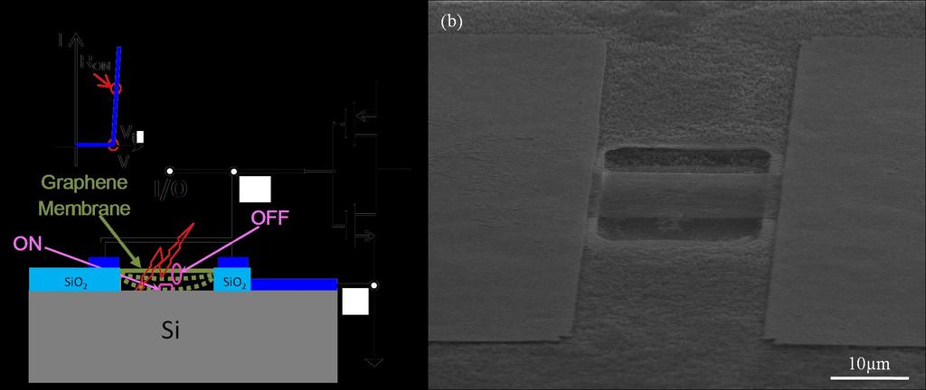
2 kv classic grounded-gate n-channel MOSFET (ggnmos) ESD device can be ~100 na, which is intolerable to advanced ICs at sub-45 nm nodes. (2) ESD events involve significant heating due to very high current surges, which require ESD protection structures to be superior in electrical and thermal conduction. (3) Advanced ESD protection require the fast response time (t 1 ) of ESD devices to be in the range of ~10-9 seconds. (4) ESD-induced parasitic capacitance (C ESD ) and noises become more severe for advanced mixed-signal and RF ICs. The demand for high performance ESD solutions with low parasitic effects hence calls for other ESD protection structures. Graphene, as a two-dimensional material with superior electrical 7 and thermal conductivity, 8 as well as mechanical strength, 9 is an excellent candidate to build ESD devices from. The high electrical conductivity of graphene promises a high current carrying capability and low heating effects. Combined with graphene's excellent thermal conductivity, the heat dissipation problem can be resolved. Moreover, graphene is known as the strongest material, which guarantees the robustness of ESD device. In this work, an electro-mechanical graphene ribbon (GR) ESD protection structure was demonstrated. In principle, zero leakage and fast response time can be achieved by using the proposed device structure. While some studies of suspended graphene devices have been previously studied, there is little information on transient characterization of suspended graphene devices for ESD protection which is different from any DC switch phenomena. Most of the previously reported suspended graphene devices were fabricated using mechanically exfoliated graphene which is impractical for wafer-scale fabrication. The fabrication process is usually delicate and involves the use of critical point drier. The process flow developed in this study uses large-area CVD grown graphene. Si 3 N 4 hard mask and a HF vapor etching technique were used to release the suspended GR rendering higher yield and device reliability. Figure 1(a) illustrates the suspended GR ESD structure for ICs. When GR is in its original suspended position, the device is in the "OFF" state with no conduction. When a bias is applied to the device, GR will be pulled down towards the bottom by the electrostatic force. If the mechanical restoring force is strong enough to balance the electrostatic force, the GR can bend and remain in a stable equilibrium position. If the bias is large enough, the GR will touch the heavily doped Si substrate, forming a 2
3 conducting path. This puts the device in the "ON" state to discharge ESD surges. The voltage at which the GR is pulled down to the bottom is the trigger voltage (V t1 ) of the ESD device. Ideally, the on-resistance (R on ) should be small for efficient ESD discharging. Since there is no conducting path when the device is in the OFF state, in principle, zero leakage can be realized. The process flow for the fabrication of the suspended GR device is as follows: First, thermal SiO 2 (wet oxidation) with desired thickness was grown at 1000 o C on heavily doped Si substrate. Second, thin layer of LPCVD Si 3 N 4 (~50 nm) was grown on top of SiO 2 to form a hard mask for the final HF vapor etching. This was followed by thermal annealing at 1100 o C in air for 1 hour to release the residual strain at the interface. This step is crucial because in the final HF vapor etching step, the residual strain will cause fast etching of SiO 2 at interface, leading to the Si 3 N 4 layer being peeled off. Third, photolithography and reactive-ion etching were used to etch away the Si 3 N 4 in the area where the chambers will be formed in the end. AZ5214 photoresist was used in the photolithography, and CHF 3 and O 2 gases were used for the plasma etching. Then CVD grown graphene was transferred onto the trenched substrate and patterned into individual GRs by photolithography and O 2 plasma etching. Next, the metal pads consisting of Ti/Pd/Au (0.5/30/50 nm) were deposited by e-beam evaporation and lift-off processes. Finally, HF vapor etching was used to etch away the exposed SiO 2 layer to release the suspended GR structure. Figure 1(b) shows a scanning electron microscopy (SEM) image of the as-fabricated device. Two-terminal DC measurements were carried out by applying a bias between top and bottom contacts. A current compliance of 0.1 ma was set to avoid device breakdown. Measurements were conducted on devices with different dimensions, i.e., the length (L) and the device trench depth (d), to characterize the turn-on behaviors. Figure 2(a) depicts the sharp turn-on of the devices affected by L with a fixed d. The measured V t1 are about 3.9, 7.2, 15.2, and 30 V for L= 7/10/15/20 µm, respectively. It seems to follow the V t1 1/L 2 relationship. 10,11 Similarly, Figure 2(b) shows the turn-on behavior of the devices with different d for a fixed L. The measured V t1 are about 3.9, 7.8, and 16 V for d= 350/550/850 nm, respectively, following a relationship of V t1 d 3/2. 11 The observed 3
 Device structure and its I-V curve. (b) SEM image of an as-fabricated device.")
4 DC switching behaviors lay the foundation for potential ESD discharging function of the proposed suspended GR ESD device. Figure 1. Suspended GR ESD device structure. (a) Device structure and its I-V curve. (b) SEM image of an as-fabricated device. Another three-terminal DC measurement set-up was used to study the mechanical shape evolution of GR as the applied bias increased. The purpose of this measurement is to measure the resistance (R) change of the GR as the bottom contact bias (V) increases, from which the bias induced charge (ΔQ), the capacitance (C) change, and the bending information of GR can be calculated and extracted. The capacitance of the device cannot be directly measured because majority of the total capacitance comes from metal contacts whereas the capacitance from GR is negligibly small (on the order of 0.1 ff). As opposed to the device for two-terminal measurement, a thin layer of SiO 2 (50 nm) was intentionally left at the bottom of the chamber in order to prevent direct contact between the GR and the Si substrate, so that R of the GR can still be measured even after it has collapsed. The measurements were conducted by simultaneously applying lateral "toptop" and vertical "top-bottom" biases. The top-top bias was kept at 5 mv to measure the resistance of GR while sweeping the top-bottom bias. The intentionally left-behind SiO 2 wouldn't affect the device performance much except for a slight decrease in the trigger voltage. Finite Element Simulations using COMSOL Multiphysics Modeling software package were conducted to compare with the experimental results. Three built-in models 4
5 were used to simulate the device behavior including Solid Mechanics, Electrostatic, and Moving Mesh. Suspended GR is viewed as an equal potential entity and the effect of quantum capacitance is assumed to be negligible. Figure 2. Two-terminal DC measurement results show ideal switching effect. (a) Devices of L= 7/10/15/20 µm with fixed d= 350 nm. (b) Devices of d= 350/550/850 nm with fixed L= 20µm. Width of GR is 5 µm. 5
6 Figure 3(a) shows the change of R as V increases (for positive bottom contact bias) for a sample device with L=20 µm and d= 300 nm. Because the GRs used in the experiments are p-type doped, as the positive bias on Si substrate increases, the Fermi level of GR goes up and R increases slowly. At a certain voltage, R increases abruptly, corresponding to the pull-in of the GR. 14 The trigger voltage is slightly smaller than that measured by the two-terminal testing due to the smaller trench depth. The bias induced excess charge per GR width (ΔQ) and capacitance per GR width (C) of GR can be calculated by, Q = L 2 WRμ (1) C = Q V (2) where Q is the total number of charges per GR width, W is the width of GR, and µ is the mobility of GR. The calculated and simulated results of ΔQ and C as a function of V are shown in Figures 3(b) and (c). Similar to the change of R, ΔQ and C increase slowly at small voltage values then increase abruptly at the pull-in voltage. When the GR is pulled in and collapsed at trench bottom, the gap between the GR and the Si substrate reaches its minimum at 50 nm, thus the capacitance reaches its peak value and remains constant thereafter. The maximum calculated and simulated capacitance are consistent with the value calculated from the geometry of the device. The experimental and simulation results fit very well with each other. Devices with dimensions of L=20 µm, d= 2 µm were also tested using the same measurement method. It is worth noting that the GR breaks at pull-in due to the very deep trench of the sample devices, and R increases dramatically. But before breaking, the calculations are still valid, and the results are similar. Assuming GR fully collapses on the trench bottom and sidewalls, the tensile strain on GR is ~20%, which is smaller than the theoretical maximum strain (25%) graphene can sustain. 15 This can be explained by the non-uniform strain distribution on the GR. 16 Next, transient TLP measurements, specific for human body model (HBM) ESD discharging testing, were conducted using a BARTH Model 4002 HBM TLP tester to characterize the fast switching behavior and reliability of the suspended GR ESD protection device. The measurements were conducted by applying a fast TLP pulse between top and bottom contacts. A rise time of 10 ns and duration time of 100 ns were used per HBM ESD testing standard. A current compliance of 2 ma was set to avoid 6
7 breakdown of the device. Similar to the two-terminal DC measurement results, sharp turn-on behavior was clearly observed as shown in Figure 4 with a V t1 ~19 V for the sample device of L= 10 µm. Unlike DC biasing, transient TLP testing is very fast, which confirms that the new GR device can switch at ns speed, critical for ESD protection. For device reliability study, repeated TLP stresses were applied to the same device over 30 times and the transient switching behavior remains. A slight change in V t1, decreasing from 19 V to 18 V after 30-time repeats of the test, was observed for the sample device, which may be due to the slight sliding of the GR caused by repetitive pulling. 17 Further studies need to be carried out to improve the device reliability, mainly in the device fabrication. Trigger voltage (V t1 ) and response time (t 1 ) are two key parameters of ESD devices. As has been discussed previously, V t1 can be tuned by modifying the device dimensions to meet specific design requirements of ICs. On the other hand, t 1 of the device can be calculated as follows: 18 t 1 = 3.67V t1 (V op f 0 ) (3) h f 0 = 1.03 E (4) ρ L 2 where V op is the operation voltage, f 0 is the resonance frequency of GR, E is the Young's modulus of graphene, ρ is the density of graphene, h is the thickness of graphene, L is the length of GR. Due to the large E and small ρ of graphene, it is a perfect fit for making fast response ESD protection devices. Theoretically, for monolayer graphene, a GR of L=300 nm could have a t 1 ~10-9 s. Multilayer graphene may be used to provide a faster response. 7
8 Figure 3. Three-terminal DC measurement and simulation results for sample devices (L= 20 µm, W= 5 µm, d= 300 nm) show the change of (a) R, (b) ΔQ and (c) C with V (positive bottom contact bias) and pull-in phenomena. 8
9 Figure 4. TLP testing shows fast turn-on behavior of a suspended GR ESD device (L= 10µm). TLP pulse rise time is 10 ns and duration is 100 ns. Moreover, design trade-offs for ESD protection devices always exist among the ESD protection level, parasitic capacitance and leakage current. Usually, higher ESD robustness means larger ESD device size, meaning more ESD-induced parasitic effects which are undesired for mixed-signal and RF ICs 2-7. Therefore, two figures of merit (FOM) are often used to evaluate the overall performance of ESD devices: FOM 1 = I t2 C ESD (5) FOM 2 = I t2 I leakage (6) where I t2, C ESD, and I leakage are the second breakdown current, ESD-induced parasitic capacitance, and leakage current, respectively. For the suspended GR device, I t2 is the breakdown current of the GR, i.e., the current carrying capability of an ESD device. I t2 was tested by TLP for both monolayer and bilayer graphene devices. The measured I t2 are about 5.5 ma and 7.5 ma for monolayer and bilayer GR devices (L= 9 µm and W= 5µm), respectively, as depicted in Figure 5. The breakdown of the devices was caused by Joule heating at high current densities and the corresponding breakdown voltages (V t2 ) were both about 12 V for monolayer and bilayer GR devices. Bilayer graphene devices show higher I t2 because both graphene layers contribute to the current conduction. For practical 9
10 ESD device design in the future, design optimization to maximize I t2 will be a key challenge in future research. 2 C ESD is the capacitance between the GR and the Si substrate and can be calculated from the device geometry. Zero OFF-state leakage current could be possible. The measured leakage was ~1 pa, presumably due to non-perfect dielectrics or surface leakage. Therefore, the FOMs of the suspended GR device samples have achieved ~14 ma/ff and ~5.5 x 10 9, which are comparable or superior to the best achievable FOMs for traditional ESD devices. We believe that I t2 of the suspended GR device can be much improved by using multilayer graphene, appropriate doping of graphene, and device encapsulation technique to provide an oxygen deficient working environment. 19,20 Device encapsulation could also prevent possible oxidation of the heavily doped Si surface and provide more stable atmospheric conditions, which are crucial for the device reliability. It is also worth noting that the device may render faster response times and higher current carrying capabilities by using multilayer graphene. However, the electrical and mechanical properties of graphene vary with film thickness, and trigger voltage will increase with the increase of graphene number of layers. Therefore, there should be an optimum film thickness per design requirements. Further research is needed on this matter. In summary, a suspended GR ESD device is reported and a fabrication process flow was developed. Both DC and transient TLP measurements were carried out for sample devices, showing the desired sharp and fast switching behaviors critical for ESD discharging operations. Measurement and simulation results match each other very well. FOMs for the sample devices achieved ~14 ma/ff (I t2 /C ESD ) and ~5.5 x 10 9 (I t2 /I leakage ), respectively. While more research is needed to further understand the ESD switching details and to improve the performance, the initial work clearly demonstrated that the suspended GR ESD device shall be a promising future ESD protection solution with advantages over traditional PN junction based ESD protection structures, including zero leakage, fast response and superior FOMs. 10
11 Figure 5. TLP testing shows breakdown characteristics for monolayer and bilayer GR devices (L= 9 µm, W=5µm). Acknowledgments This work was supported in partial by NSF under the awards and Y. H. X. acknowledges the support from Alexander von Humboldt Foundation Research Award. References 1. A. Wang, On-Chip ESD Protection for Integrated Circuits; Kluwer, Boston, A. Wang, H. Feng, R. Zhan, H. Xie, G. Chen, Q. Wu, X. Guan, Z. Wang, and C. Zhang, IEEE Trans. Electron Devices 52, 1304 (2005). 3. Z. Shi, X. Wang, J. Liu, L. Lin, H. Zhao, Q. Fang, L. Wang, C. Zhang, S. Fan, H. Tang, B. Li, A. Wang, J. Liu, and Y. Cheng, IEEE Trans. Nanotechnology 11, 884 (2012). 4. L. Wang, X. Wang, Z. Shi, R. Ma, J. Liu, Z. Dong, C. Zhang, L. Lin, H. Zhao, L. Zhang, A. Wang, Y. Cheng, and R. Huang, IEEE Electron Device Lett. 34, 111 (2013). 5. C. Zhang, Z. Dong, F. Lu, R. Ma, L. Wang, H. Zhao, X. Wang, X. S. Wang, H. Tang, and A. Wang, IEEE Electron Device Lett. 35, 381 (2014). 11
12 6. X. S. Wang, X. Wang, F. Lu, C. Zhang, Z. Dong, L. Wang, R. Ma, Z. Shi, A. Wang, M.-C. F. Chang, et al. IEEE J. Solid-State Circuits 49, 1927 (2014). 7. K. S. Novoselov, A. K. Geim, S. V. Morozov, D. Jiang, Y. Zhang, S. V. Dubonos, I. V. Grigorieva, and A. A. Firsov, Science 306, 666 (2004). 8. E. Pop, V. Varshney, and A. K. Roy, MRS Bull. 37, 1273 (2012). 9. I. A. Ovidko, Rev. Adv. Mater. Sci. 34, 1 (2013). 10. S. M. Kim, E. B. Song, S. Lee, S. Seo, D. H. Seo, Y. Hwang, R. Candler, and K. L. Wang, Appl. Phys. Lett. 99, (2011). 11. P. Li, Z. You, G. Haugstad, and T. Cui, Appl. Phys. Lett. 98, (2011). 12. Z. Shi, H. Lu, L. Zhang, R. Yang, Y. Wang, D. Liu, H. Guo, D. Shi, H. Gao, E. Wang, and G. Zhang, Nano Res. 5, 82 (2012). 13. M.-W. Lin, C. Ling, Y. Zhang, H. J. Yoon, M. M.-C. Cheng, L. A. Agapito, N. Kioussis, N. Widjaja, and Z. Zhou, Nanotechnology 22, (2011). 14. O. Bochobza-Degani, and Y. Nemirovsky, Sens. Actuators A 97-98, 569 (2002). 15. G. Cocco, E. Cadelano, and L. Colombo, Phys. Rev. B 81, (2010). 16. A. D. Smith, S. Vaziri, A. Delin, M. Ostling, and M. C. Lemme, presented in part at 13th International Conference on Ultimate Integration on Silicon (ULIS), Grenoble, March, W. Bao, K. Myhro, Z. Zhao, Z. Chen, W. Jang, L. Jing, F. Miao, H. Zhang, C. Dames, and C. N. Lau, Nano Lett.12, 5470 (2012). 18. J. B. Muldavin, and G. M. Rebeiz, IEEE MTT-S Digest 3, 2119 (2001). 19. X. Chen, D. H. Seo, S. Seo, H. Chung, and H.-S. P. Wong, IEEE Electron Device Lett. 33, 1604 (2012). 20. C. G. Kang, S. K. Lee, Y. G. Lee, H. J. Hwang, C. Cho, S. K. Lim, J. Heo, H.-J. Chung, H. Yang, S. Seo, and B. H. Lee, IEEE Electron Device Lett. 32, 1591 (2011). 12
13
14
15
16
17
Intrinsic Electronic Transport Properties of High. Information
 Intrinsic Electronic Transport Properties of High Quality and MoS 2 : Supporting Information Britton W. H. Baugher, Hugh O. H. Churchill, Yafang Yang, and Pablo Jarillo-Herrero Department of Physics, Massachusetts
Tunneling characteristics of graphene
 Tunneling characteristics of graphene Young Jun Shin, 1,2 Gopinadhan Kalon, 1,2 Jaesung Son, 1 Jae Hyun Kwon, 1,2 Jing Niu, 1 Charanjit S. Bhatia, 1 Gengchiau Liang, 1 and Hyunsoo Yang 1,2,a) 1 Department
Lecture 150 Basic IC Processes (10/10/01) Page ECE Analog Integrated Circuits and Systems P.E. Allen
 Page ECE Analog Integrated Circuits and Systems P.E. Allen") Lecture 150 Basic IC Processes (10/10/01) Page 1501 LECTURE 150 BASIC IC PROCESSES (READING: TextSec. 2.2) INTRODUCTION Objective The objective of this presentation is: 1.) Introduce the fabrication of
Lecture 150 Basic IC Processes (10/10/01) Page 1501 LECTURE 150 BASIC IC PROCESSES (READING: TextSec. 2.2) INTRODUCTION Objective The objective of this presentation is: 1.) Introduce the fabrication of
GHZ ELECTRICAL PROPERTIES OF CARBON NANOTUBES ON SILICON DIOXIDE MICRO BRIDGES
 GHZ ELECTRICAL PROPERTIES OF CARBON NANOTUBES ON SILICON DIOXIDE MICRO BRIDGES SHENG F. YEN 1, HAROON LAIS 1, ZHEN YU 1, SHENGDONG LI 1, WILLIAM C. TANG 1,2, AND PETER J. BURKE 1,2 1 Electrical Engineering
Supporting Information. by Hexagonal Boron Nitride
 Supporting Information High Velocity Saturation in Graphene Encapsulated by Hexagonal Boron Nitride Megan A. Yamoah 1,2,, Wenmin Yang 1,3, Eric Pop 4,5,6, David Goldhaber-Gordon 1 * 1 Department of Physics,
SUPPLEMENTARY INFORMATION
 doi:.38/nature09979 I. Graphene material growth and transistor fabrication Top-gated graphene RF transistors were fabricated based on chemical vapor deposition (CVD) grown graphene on copper (Cu). Cu foil
Supplementary Information for
 Supplementary Information for Highly Stable, Dual-Gated MoS 2 Transistors Encapsulated by Hexagonal Boron Nitride with Gate-Controllable Contact Resistance and Threshold Voltage Gwan-Hyoung Lee, Xu Cui,
M R S Internet Journal of Nitride Semiconductor Research
 Page 1 of 6 M R S Internet Journal of Nitride Semiconductor Research Volume 9, Article 7 The Ambient Temperature Effect on Current-Voltage Characteristics of Surface-Passivated GaN-Based Field-Effect Transistors
Supporting Infromation
 Supporting Infromation Transparent and Flexible Self-Charging Power Film and Its Application in Sliding-Unlock System in Touchpad Technology Jianjun Luo 1,#, Wei Tang 1,#, Feng Ru Fan 1, Chaofeng Liu 1,
Lithography-free Fabrication of High Quality Substrate-supported and. Freestanding Graphene devices
 Lithography-free Fabrication of High Quality Substrate-supported and Freestanding Graphene devices W. Bao 1, G. Liu 1, Z. Zhao 1, H. Zhang 1, D. Yan 2, A. Deshpande 3, B.J. LeRoy 3 and C.N. Lau 1, * 1
Supplementary Figure S1. AFM images of GraNRs grown with standard growth process. Each of these pictures show GraNRs prepared independently,
 Supplementary Figure S1. AFM images of GraNRs grown with standard growth process. Each of these pictures show GraNRs prepared independently, suggesting that the results is reproducible. Supplementary Figure
Ambipolar bistable switching effect of graphene
 Ambipolar bistable switching effect of graphene Young Jun Shin, 1,2 Jae Hyun Kwon, 1,2 Gopinadhan Kalon, 1,2 Kai-Tak Lam, 1 Charanjit S. Bhatia, 1 Gengchiau Liang, 1 and Hyunsoo Yang 1,2,a) 1 Department
Supporting Online Material for
 www.sciencemag.org/cgi/content/full/327/5966/662/dc Supporting Online Material for 00-GHz Transistors from Wafer-Scale Epitaxial Graphene Y.-M. Lin,* C. Dimitrakopoulos, K. A. Jenkins, D. B. Farmer, H.-Y.
DEPOSITION OF THIN TiO 2 FILMS BY DC MAGNETRON SPUTTERING METHOD
 Chapter 4 DEPOSITION OF THIN TiO 2 FILMS BY DC MAGNETRON SPUTTERING METHOD 4.1 INTRODUCTION Sputter deposition process is another old technique being used in modern semiconductor industries. Sputtering
Figure 1: Graphene release, transfer and stacking processes. The graphene stacking began with CVD
 Supplementary figure 1 Graphene Growth and Transfer Graphene PMMA FeCl 3 DI water Copper foil CVD growth Back side etch PMMA coating Copper etch in 0.25M FeCl 3 DI water rinse 1 st transfer DI water 1:10
SUPPLEMENTARY INFORMATION
 In the format provided by the authors and unedited. DOI: 10.1038/NPHOTON.2016.254 Measurement of non-monotonic Casimir forces between silicon nanostructures Supplementary information L. Tang 1, M. Wang
SUPPLEMENTARY NOTES Supplementary Note 1: Fabrication of Scanning Thermal Microscopy Probes
 SUPPLEMENTARY NOTES Supplementary Note 1: Fabrication of Scanning Thermal Microscopy Probes Fabrication of the scanning thermal microscopy (SThM) probes is summarized in Supplementary Fig. 1 and proceeds
Ambipolar Graphene Field Effect Transistors by Local Metal Side Gates USA. Indiana 47907, USA. Abstract
 Ambipolar Graphene Field Effect Transistors by Local Metal Side Gates J. F. Tian *, a, b, L. A. Jauregui c, b, G. Lopez c, b, H. Cao a, b *, a, b, c, and Y. P. Chen a Department of Physics, Purdue University,
Compound buried layer SOI high voltage device with a step buried oxide
 Compound buried layer SOI high voltage device with a step buried oxide Wang Yuan-Gang( ), Luo Xiao-Rong( ), Ge Rui( ), Wu Li-Juan( ), Chen Xi( ), Yao Guo-Liang( ), Lei Tian-Fei( ), Wang Qi( ), Fan Jie(
Graphene devices and integration: A primer on challenges
 Graphene devices and integration: A primer on challenges Archana Venugopal (TI) 8 Nov 2016 Acknowledgments: Luigi Colombo (TI) UT Dallas and UT Austin 1 Outline Where we are Issues o Contact resistance
2D Materials for Gas Sensing
 2D Materials for Gas Sensing S. Guo, A. Rani, and M.E. Zaghloul Department of Electrical and Computer Engineering The George Washington University, Washington DC 20052 Outline Background Structures of
Frequency dispersion effect and parameters. extraction method for novel HfO 2 as gate dielectric
 048 SCIENCE CHINA Information Sciences April 2010 Vol. 53 No. 4: 878 884 doi: 10.1007/s11432-010-0079-8 Frequency dispersion effect and parameters extraction method for novel HfO 2 as gate dielectric LIU
Traps in MOCVD n-gan Studied by Deep Level Transient Spectroscopy and Minority Carrier Transient Spectroscopy
 Traps in MOCVD n-gan Studied by Deep Level Transient Spectroscopy and Minority Carrier Transient Spectroscopy Yutaka Tokuda Department of Electrical and Electronics Engineering, Aichi Institute of Technology,
RF Performance Projections of Graphene FETs vs. Silicon MOSFETs
 1 RF Performance Projections of Graphene FETs vs. Silicon MOSFETs S. Rodriguez *, S. Vaziri *, M. Ostling *, A. Rusu *, E. Alarcon *,#, M.C. Lemme *1 * KTH Royal Institute of Technology, School of ICT,
Theoretical Study on Graphene Silicon Heterojunction Solar Cell
 Copyright 2015 American Scientific Publishers All rights reserved Printed in the United States of America Journal of Nanoelectronics and Optoelectronics Vol. 10, 1 5, 2015 Theoretical Study on Graphene
Understanding the effect of n-type and p-type doping in the channel of graphene nanoribbon transistor
 Bull. Mater. Sci., Vol. 39, No. 5, September 2016, pp. 1303 1309. DOI 10.1007/s12034-016-1277-9 c Indian Academy of Sciences. Understanding the effect of n-type and p-type doping in the channel of graphene
Supporting Information
 Supporting Information Monolithically Integrated Flexible Black Phosphorus Complementary Inverter Circuits Yuanda Liu, and Kah-Wee Ang* Department of Electrical and Computer Engineering National University
Fabrication Technology, Part I
 EEL5225: Principles of MEMS Transducers (Fall 2004) Fabrication Technology, Part I Agenda: Microfabrication Overview Basic semiconductor devices Materials Key processes Oxidation Thin-film Deposition Reading:
Hybrid Surface-Phonon-Plasmon Polariton Modes in Graphene /
 Supplementary Information: Hybrid Surface-Phonon-Plasmon Polariton Modes in Graphene / Monolayer h-bn stacks Victor W. Brar 1,2, Min Seok Jang 3,, Michelle Sherrott 1, Seyoon Kim 1, Josue J. Lopez 1, Laura
Supporting Information
 Electronic Supplementary Material (ESI) for Nanoscale. This journal is The Royal Society of Chemistry 2016 Supporting Information Graphene transfer method 1 : Monolayer graphene was pre-deposited on both
Sub-5 nm Patterning and Applications by Nanoimprint Lithography and Helium Ion Beam Lithography
 Sub-5 nm Patterning and Applications by Nanoimprint Lithography and Helium Ion Beam Lithography Yuanrui Li 1, Ahmed Abbas 1, Yuhan Yao 1, Yifei Wang 1, Wen-Di Li 2, Chongwu Zhou 1 and Wei Wu 1* 1 Department
Supplementary Information
 Supplementary Information Supplementary Figure 1 Raman spectroscopy of CVD graphene on SiO 2 /Si substrate. Integrated Raman intensity maps of D, G, 2D peaks, scanned across the same graphene area. Scale
Stretching the Barriers An analysis of MOSFET Scaling. Presenters (in order) Zeinab Mousavi Stephanie Teich-McGoldrick Aseem Jain Jaspreet Wadhwa
 Zeinab Mousavi Stephanie Teich-McGoldrick Aseem Jain Jaspreet Wadhwa") Stretching the Barriers An analysis of MOSFET Scaling Presenters (in order) Zeinab Mousavi Stephanie Teich-McGoldrick Aseem Jain Jaspreet Wadhwa Why Small? Higher Current Lower Gate Capacitance Higher
Stretching the Barriers An analysis of MOSFET Scaling Presenters (in order) Zeinab Mousavi Stephanie Teich-McGoldrick Aseem Jain Jaspreet Wadhwa Why Small? Higher Current Lower Gate Capacitance Higher
Asymmetrical heating behavior of doped Si channels in bulk silicon and in silicon-on-insulator under high current stress
 JOURNAL OF APPLIED PHYSICS VOLUME 86, NUMBER 12 15 DECEMBER 1999 Asymmetrical heating behavior of doped Si channels in bulk silicon and in silicon-on-insulator under high current stress C. N. Liao, a)
SUPPLEMENTARY INFORMATION. Observation of tunable electrical bandgap in large-area twisted bilayer graphene synthesized by chemical vapor deposition
 SUPPLEMENTARY INFORMATION Observation of tunable electrical bandgap in large-area twisted bilayer graphene synthesized by chemical vapor deposition Jing-Bo Liu 1 *, Ping-Jian Li 1 *, Yuan-Fu Chen 1, Ze-Gao
Lithography-Free Fabrication of High Quality Substrate- Supported and Freestanding Graphene Devices
 98 DOI 10.1007/s12274-010-1013-5 Research Article Lithography-Free Fabrication of High Quality Substrate- Supported and Freestanding Graphene Devices Wenzhong Bao 1, Gang Liu 1, Zeng Zhao 1, Hang Zhang
Inkjet Printed Highly Transparent and Flexible Graphene Micro- Supercapacitors
 Electronic Supplementary Material (ESI) for Nanoscale. This journal is The Royal Society of Chemistry 2017 Inkjet Printed Highly Transparent and Flexible Graphene Micro- Supercapacitors Szymon Sollami
Analyses of LiNbO 3 wafer surface etched by ECR plasma of CHF 3 & CF 4
 1998 DRY PROCESS SYMPOSIUM VI - 3 Analyses of LiNbO 3 wafer surface etched by ECR plasma of CHF 3 & CF 4 Naoki Mitsugi, Kaori Shima, Masumi Ishizuka and Hirotoshi Nagata New Technology Research Laboratories,
Graphene Chemical Vapor Deposition (CVD) Growth
 Growth") ECE440 Nanoelectronics Graphene Chemical Vapor Deposition (CVD) Growth Zheng Yang Timeline of graphene CVD growth Exfoliation
ECE440 Nanoelectronics Graphene Chemical Vapor Deposition (CVD) Growth Zheng Yang Timeline of graphene CVD growth Exfoliation
NiCl2 Solution concentration. Etching Duration. Aspect ratio. Experiment Atmosphere Temperature. Length(µm) Width (nm) Ar:H2=9:1, 150Pa
 Width (nm) Ar:H2=9:1, 150Pa") Experiment Atmosphere Temperature #1 # 2 # 3 # 4 # 5 # 6 # 7 # 8 # 9 # 10 Ar:H2=9:1, 150Pa Ar:H2=9:1, 150Pa Ar:H2=9:1, 150Pa Ar:H2=9:1, 150Pa Ar:H2=9:1, 150Pa Ar:H2=9:1, 150Pa Ar:H2=9:1, 150Pa Ar:H2=9:1,
Experiment Atmosphere Temperature #1 # 2 # 3 # 4 # 5 # 6 # 7 # 8 # 9 # 10 Ar:H2=9:1, 150Pa Ar:H2=9:1, 150Pa Ar:H2=9:1, 150Pa Ar:H2=9:1, 150Pa Ar:H2=9:1, 150Pa Ar:H2=9:1, 150Pa Ar:H2=9:1, 150Pa Ar:H2=9:1,
Graphene Transistors Fabricated via Transfer-Printing In Device Active-Areas on Large Wafer
 Graphene Transistors Fabricated via Transfer-Printing In Device Active-Areas on Large Wafer NANO LETTERS 2007 Vol. 7, No. 12 3840-3844 Xiaogan Liang, Zengli Fu, and Stephen Y. Chou* NanoStructure Laboratory,
Supplementary material for High responsivity mid-infrared graphene detectors with antenna-enhanced photo-carrier generation and collection
 Supplementary material for High responsivity mid-infrared graphene detectors with antenna-enhanced photo-carrier generation and collection Yu Yao 1, Raji Shankar 1, Patrick Rauter 1, Yi Song 2, Jing Kong
Wafer-scale fabrication of graphene
 Wafer-scale fabrication of graphene Sten Vollebregt, MSc Delft University of Technology, Delft Institute of Mircosystems and Nanotechnology Delft University of Technology Challenge the future Delft University
The role of charge traps in inducing hysteresis: capacitance voltage measurements on top gated bilayer graphene
 The role of charge traps in inducing hysteresis: capacitance voltage measurements on top gated bilayer graphene Gopinadhan Kalon, Young Jun Shin, Viet Giang Truong, Alan Kalitsov, and Hyunsoo Yang a) Department
Rectification in a Black Phosphorus/WS2 van der. Waals Heterojunction Diode
 Supporting Information Temperature-Dependent and Gate-Tunable Rectification in a Black Phosphorus/WS2 van der Waals Heterojunction Diode Ghulam Dastgeer 1, Muhammad Farooq Khan 1, Ghazanfar Nazir 1, Amir
Lecture 12: MOS Capacitors, transistors. Context
 Lecture 12: MOS Capacitors, transistors Context In the last lecture, we discussed PN diodes, and the depletion layer into semiconductor surfaces. Small signal models In this lecture, we will apply those
Precision Cutting and Patterning of Graphene with Helium Ions. 1.School of Engineering and Applied Sciences, Harvard University, Cambridge MA 02138
 Precision Cutting and Patterning of Graphene with Helium Ions D.C. Bell 1,2, M.C. Lemme 3, L. A. Stern 4, J.R. Williams 1,3, C. M. Marcus 3 1.School of Engineering and Applied Sciences, Harvard University,
Electrostatics of Nanowire Transistors
 Electrostatics of Nanowire Transistors Jing Guo, Jing Wang, Eric Polizzi, Supriyo Datta and Mark Lundstrom School of Electrical and Computer Engineering Purdue University, West Lafayette, IN, 47907 ABSTRACTS
Supplementary information for
 Supplementary information for Transverse electric field dragging of DNA in a nanochannel Makusu Tsutsui, Yuhui He, Masayuki Furuhashi, Rahong Sakon, Masateru Taniguchi & Tomoji Kawai The Supplementary
nmos IC Design Report Module: EEE 112
 nmos IC Design Report Author: 1302509 Zhao Ruimin Module: EEE 112 Lecturer: Date: Dr.Zhao Ce Zhou June/5/2015 Abstract This lab intended to train the experimental skills of the layout designing of the
Supplementary Figure 1 Dark-field optical images of as prepared PMMA-assisted transferred CVD graphene films on silicon substrates (a) and the one
 and the one") Supplementary Figure 1 Dark-field optical images of as prepared PMMA-assisted transferred CVD graphene films on silicon substrates (a) and the one after PBASE monolayer growth (b). 1 Supplementary Figure
Supplementary Figure 1 Dark-field optical images of as prepared PMMA-assisted transferred CVD graphene films on silicon substrates (a) and the one after PBASE monolayer growth (b). 1 Supplementary Figure
Nanoelectronics. Topics
 Nanoelectronics Topics Moore s Law Inorganic nanoelectronic devices Resonant tunneling Quantum dots Single electron transistors Motivation for molecular electronics The review article Overview of Nanoelectronic
Controlling Graphene Ultrafast Hot Carrier Response from Metal-like. to Semiconductor-like by Electrostatic Gating
 Controlling Graphene Ultrafast Hot Carrier Response from Metal-like to Semiconductor-like by Electrostatic Gating S.-F. Shi, 1,2* T.-T. Tang, 1 B. Zeng, 1 L. Ju, 1 Q. Zhou, 1 A. Zettl, 1,2,3 F. Wang 1,2,3
Strain-induced programmable half-metal and spin-gapless semiconductor in an edge-doped boron nitride nanoribbon
 Strain-induced programmable half-metal and spin-gapless semiconductor in an edge-doped boron nitride nanoribbon Shuze Zhu 1, Teng Li 1 Department of Mechanical Engineering, University of Maryland, College
Supporting Information for: Sustained sub-60 mv/decade switching via the negative capacitance effect in MoS 2 transistors
 Supporting Information for: Sustained sub-60 mv/decade switching via the negative capacitance effect in MoS 2 transistors Felicia A. McGuire 1, Yuh-Chen Lin 1, Katherine Price 1, G. Bruce Rayner 2, Sourabh
CMOS Logic Gates. University of Connecticut 172
 CMOS Logic Gates University of Connecticut 172 Basic CMOS Inverter Operation V IN P O N O p-channel enhancementtype MOSFET; V T < 0 n-channel enhancementtype MOSFET; V T > 0 If V IN 0, N O is cut off and
Supplementary Figures
 Supplementary Figures Supplementary Figure 1 Molecular structures of functional materials involved in our SGOTFT devices. Supplementary Figure 2 Capacitance measurements of a SGOTFT device. (a) Capacitance
Transient Harman Measurement of the Cross-plane ZT of InGaAs/InGaAlAs Superlattices with Embedded ErAs Nanoparticles
 Transient Harman Measurement of the Cross-plane ZT of InGaAs/InGaAlAs Superlattices with Embedded ErAs Nanoparticles Rajeev Singh, Zhixi Bian, Gehong Zeng, Joshua Zide, James Christofferson, Hsu-Feng Chou,
Flexible Asymmetrical Solid-state Supercapacitors Based on Laboratory Filter Paper
 SUPPORTING INFORMATION Flexible Asymmetrical Solid-state Supercapacitors Based on Laboratory Filter Paper Leicong Zhang,,,# Pengli Zhu,,,#, * Fengrui Zhou, Wenjin Zeng, Haibo Su, Gang Li, Jihua Gao, Rong
Selective Manipulation of Molecules by Electrostatic Force and Detection of Single Molecules in Aqueous Solution
 Supporting Information Selective Manipulation of Molecules by Electrostatic Force and Detection of Single Molecules in Aqueous Solution Zhongbo Yan, Ming Xia, Pei Zhang, and Ya-Hong Xie* Department of
Modeling of the Substrate Current and Characterization of Traps in MOSFETs under Sub-Bandgap Photonic Excitation
 Journal of the Korean Physical Society, Vol. 45, No. 5, November 2004, pp. 1283 1287 Modeling of the Substrate Current and Characterization of Traps in MOSFETs under Sub-Bandgap Photonic Excitation I.
UNIVERSITY OF CALIFORNIA College of Engineering Department of Electrical Engineering and Computer Sciences. Professor Chenming Hu.
 UNIVERSITY OF CALIFORNIA College of Engineering Department of Electrical Engineering and Computer Sciences EECS 130 Spring 2009 Professor Chenming Hu Midterm I Name: Closed book. One sheet of notes is
6.012 Electronic Devices and Circuits
 Page 1 of 10 YOUR NAME Department of Electrical Engineering and Computer Science Massachusetts Institute of Technology 6.012 Electronic Devices and Circuits Exam No. 2 Thursday, November 5, 2009 7:30 to
Nanocarbon Interconnects - From 1D to 3D
 Nanocarbon Interconnects - From 1D to 3D Cary Y. Yang Santa Clara University Outline Introduction CNT as 1D interconnect structure CNT-graphene as all-carbon 3D interconnect Summary Device Scaling driven
1. Nanotechnology & nanomaterials -- Functional nanomaterials enabled by nanotechnologies.
 Novel Nano-Engineered Semiconductors for Possible Photon Sources and Detectors NAI-CHANG YEH Department of Physics, California Institute of Technology 1. Nanotechnology & nanomaterials -- Functional nanomaterials
Improved Interfacial and Electrical Properties of GaSb Metal Oxide
 Improved Interfacial and Electrical Properties of GaSb Metal Oxide Semiconductor Devices Passivated with Acidic (NH 4 ) 2 S Solution Lianfeng Zhao, Zhen Tan, Jing Wang, and Jun Xu * Tsinghua National Laboratory
Half-Integer Quantum Conductance States
 Supporting Information A 50 mv Cu/SiO /W Memristor with Half-Integer Quantum Conductance States S. R. Nandakumar, Marie Minvielle, Saurabh Nagar, Catherine Dubourdieu, and Bipin Rajendran, Department of
Flexible Piezoelectric-Induced Pressure Sensors for Static. Measurements Based on Nanowires/Graphene Heterostructures
 Flexible Piezoelectric-Induced Pressure Sensors for Static Measurements Based on Nanowires/Graphene Heterostructures Zefeng Chen,, Zhao Wang,, Xinming Li,*, Yuxuan Lin, Ningqi Luo, Mingzhu Long, Ni Zhao,
Schottky Rectifiers Zheng Yang (ERF 3017,
 ECE442 Power Semiconductor Devices and Integrated Circuits Schottky Rectifiers Zheng Yang (ERF 3017, email: yangzhen@uic.edu) Power Schottky Rectifier Structure 2 Metal-Semiconductor Contact The work function
Transient Photocurrent Measurements of Graphene Related Materials
 Transient Photocurrent Measurements of Graphene Related Materials P. Srinivasa Rao Mentor: Prof. dr. Gvido Bratina Laboratory of Organic Matter Physics University of Nova Gorica 1 Contents: 1. Electrical
Supporting Information. Fast Synthesis of High-Performance Graphene by Rapid Thermal Chemical Vapor Deposition
 1 Supporting Information Fast Synthesis of High-Performance Graphene by Rapid Thermal Chemical Vapor Deposition Jaechul Ryu, 1,2, Youngsoo Kim, 4, Dongkwan Won, 1 Nayoung Kim, 1 Jin Sung Park, 1 Eun-Kyu
SUPPLEMENTARY INFORMATION
 SUPPLEMENTARY INFORMATION Facile Synthesis of High Quality Graphene Nanoribbons Liying Jiao, Xinran Wang, Georgi Diankov, Hailiang Wang & Hongjie Dai* Supplementary Information 1. Photograph of graphene
CMOS Logic Gates. University of Connecticut 181
 CMOS Logic Gates University of Connecticut 181 Basic CMOS Inverter Operation V IN P O N O p-channel enhancementtype MOSFET; V T < 0 n-channel enhancementtype MOSFET; V T > 0 If V IN 0, N O is cut off and
Effective Capacitance Enhancement Methods for 90-nm DRAM Capacitors
 Journal of the Korean Physical Society, Vol. 44, No. 1, January 2004, pp. 112 116 Effective Capacitance Enhancement Methods for 90-nm DRAM Capacitors Y. K. Park, Y. S. Ahn, S. B. Kim, K. H. Lee, C. H.
Self-study problems and questions Processing and Device Technology, FFF110/FYSD13
 Self-study problems and questions Processing and Device Technology, FFF110/FYSD13 Version 2016_01 In addition to the problems discussed at the seminars and at the lectures, you can use this set of problems
Graphene Novel Material for Nanoelectronics
 Graphene Novel Material for Nanoelectronics Shintaro Sato Naoki Harada Daiyu Kondo Mari Ohfuchi (Manuscript received May 12, 2009) Graphene is a flat monolayer of carbon atoms with a two-dimensional honeycomb
Supporting information
 Supporting information Design, Modeling and Fabrication of CVD Grown MoS 2 Circuits with E-Mode FETs for Large-Area Electronics Lili Yu 1*, Dina El-Damak 1*, Ujwal Radhakrishna 1, Xi Ling 1, Ahmad Zubair
Stabilizing the forming process in unipolar resistance switching
 Stabilizing the forming process in unipolar resistance switching using an improved compliance current limiter S. B. Lee, 1 S. H. Chang, 1 H. K. Yoo, 1 and B. S. Kang 2,a) 1 ReCFI, Department of Physics
Resistance Thermometry based Picowatt-Resolution Heat-Flow Calorimeter
 Resistance Thermometry based Picowatt-Resolution Heat-Flow Calorimeter S. Sadat 1, E. Meyhofer 1 and P. Reddy 1, 1 Department of Mechanical Engineering, University of Michigan, Ann Arbor, 48109 Department
TRANSVERSE SPIN TRANSPORT IN GRAPHENE
 International Journal of Modern Physics B Vol. 23, Nos. 12 & 13 (2009) 2641 2646 World Scientific Publishing Company TRANSVERSE SPIN TRANSPORT IN GRAPHENE TARIQ M. G. MOHIUDDIN, A. A. ZHUKOV, D. C. ELIAS,
Efficient Preparation of Large-Area Graphene Oxide Sheets for Transparent Conductive Films
 Supporting Information Efficient Preparation of Large-Area Graphene Oxide Sheets for Transparent Conductive Films Jinping Zhao, Songfeng Pei, Wencai Ren*, Libo Gao and Hui-Ming Cheng* Shenyang National
Benefits of Stacked-Wafer Capacitors for High-Frequency Buck Converters
 Benefits of Stacked-Wafer Capacitors for High-Frequency Buck Converters Michael W. Baker, PhD Maxim Integrated Power SoC Northeastern University, Boston MA. October 7, 2014 Mobile Device Trends Power Management
Lecture 0: Introduction
 Lecture 0: Introduction Introduction q Integrated circuits: many transistors on one chip q Very Large Scale Integration (VLSI): bucketloads! q Complementary Metal Oxide Semiconductor Fast, cheap, low power
Application Note. Graphene Characterization by Correlation of Scanning Electron, Atomic Force and Interference Contrast Microscopy
 Graphene Characterization by Correlation of Scanning Electron, Atomic Force and Interference Contrast Microscopy Graphene Characterization by Correlation of Scanning Electron, Atomic Force and Interference
Supplementary Methods A. Sample fabrication
 Supplementary Methods A. Sample fabrication Supplementary Figure 1(a) shows the SEM photograph of a typical sample, with three suspended graphene resonators in an array. The cross-section schematic is
Woo Jin Hyun, Ethan B. Secor, Mark C. Hersam, C. Daniel Frisbie,* and Lorraine F. Francis*
 Woo Jin Hyun, Ethan B. Secor, Mark C. Hersam, C. Daniel Frisbie,* and Lorraine F. Francis* Dr. W. J. Hyun, Prof. C. D. Frisbie, Prof. L. F. Francis Department of Chemical Engineering and Materials Science
TEA10402V15A0 Engineering Specification
 TEA10402V15A0 Engineering 1. Scope This specification is applied to electrostatic discharge (ESD) protection. It is designed to protect the high-speed data lines against ESD transients. It has very low
SUPPLEMENTARY INFORMATION
 SUPPLEMENTARY INFORMATION Controlled Ripple Texturing of Suspended Graphene and Ultrathin Graphite Membranes Wenzhong Bao, Feng Miao, Zhen Chen, Hang Zhang, Wanyoung Jang, Chris Dames, Chun Ning Lau *
Electro-Thermal Transport in Silicon and Carbon Nanotube Devices E. Pop, D. Mann, J. Rowlette, K. Goodson and H. Dai
 Electro-Thermal Transport in Silicon and Carbon Nanotube Devices E. Pop, D. Mann, J. Rowlette, K. Goodson and H. Dai E. Pop, 1,2 D. Mann, 1 J. Rowlette, 2 K. Goodson 2 and H. Dai 1 Dept. of 1 Chemistry
A Bottom-gate Depletion-mode Nanowire Field Effect Transistor (NWFET) Model Including a Schottky Diode Model
 Model Including a Schottky Diode Model") Journal of the Korean Physical Society, Vol. 55, No. 3, September 2009, pp. 1162 1166 A Bottom-gate Depletion-mode Nanowire Field Effect Transistor (NWFET) Model Including a Schottky Diode Model Y. S.
Journal of the Korean Physical Society, Vol. 55, No. 3, September 2009, pp. 1162 1166 A Bottom-gate Depletion-mode Nanowire Field Effect Transistor (NWFET) Model Including a Schottky Diode Model Y. S.
crystals were phase-pure as determined by x-ray diffraction. Atomically thin MoS 2 flakes were
 Nano Letters (214) Supplementary Information for High Mobility WSe 2 p- and n-type Field Effect Transistors Contacted by Highly Doped Graphene for Low-Resistance Contacts Hsun-Jen Chuang, Xuebin Tan, Nirmal
Graphene photodetectors with ultra-broadband and high responsivity at room temperature
 SUPPLEMENTARY INFORMATION DOI: 10.1038/NNANO.2014.31 Graphene photodetectors with ultra-broadband and high responsivity at room temperature Chang-Hua Liu 1, You-Chia Chang 2, Ted Norris 1.2* and Zhaohui
Thermo-structural Model of Stacked Field-programmable Gate Arrays (FPGAs) with Through-silicon Vias (TSVs)
 with Through-silicon Vias (TSVs)") Manuscript for Review Thermo-structural Model of Stacked Field-programmable Gate Arrays (FPGAs) with Through-silicon Vias (TSVs) Journal: Electronics Letters Manuscript ID: draft Manuscript Type: Letter
Manuscript for Review Thermo-structural Model of Stacked Field-programmable Gate Arrays (FPGAs) with Through-silicon Vias (TSVs) Journal: Electronics Letters Manuscript ID: draft Manuscript Type: Letter
Chapter 3 Basics Semiconductor Devices and Processing
 Chapter 3 Basics Semiconductor Devices and Processing Hong Xiao, Ph. D. www2.austin.cc.tx.us/hongxiao/book.htm Hong Xiao, Ph. D. www2.austin.cc.tx.us/hongxiao/book.htm 1 Objectives Identify at least two
Monolayer Semiconductors
 Monolayer Semiconductors Gilbert Arias California State University San Bernardino University of Washington INT REU, 2013 Advisor: Xiaodong Xu (Dated: August 24, 2013) Abstract Silicon may be unable to
Normally-Off GaN Field Effect Power Transistors: Device Design and Process Technology Development
 Center for High Performance Power Electronics Normally-Off GaN Field Effect Power Transistors: Device Design and Process Technology Development Dr. Wu Lu (614-292-3462, lu.173@osu.edu) Dr. Siddharth Rajan
Large Scale Direct Synthesis of Graphene on Sapphire and Transfer-free Device Fabrication
 Supplementary Information Large Scale Direct Synthesis of Graphene on Sapphire and Transfer-free Device Fabrication Hyun Jae Song a, Minhyeok Son a, Chibeom Park a, Hyunseob Lim a, Mark P. Levendorf b,
Novel Back-Biased UTBB Lateral SCR for FDSOI ESD Protections
 Novel Back-Biased UTBB Lateral SCR for FDSOI ESD Protections Yohann Solaro 1,2,3, Pascal Fonteneau 1, Charles-Alexandre Legrand 1 Claire Fenouillet-Beranger 1,3, Philippe Ferrari 2, Sorin Cristoloveanu
Large Storage Window in a-sinx/nc-si/a-sinx Sandwiched Structure
 2017 Asia-Pacific Engineering and Technology Conference (APETC 2017) ISBN: 978-1-60595-443-1 Large Storage Window in a-sinx/nc-si/a-sinx Sandwiched Structure Xiang Wang and Chao Song ABSTRACT The a-sin
Final Examination EE 130 December 16, 1997 Time allotted: 180 minutes
 Final Examination EE 130 December 16, 1997 Time allotted: 180 minutes Problem 1: Semiconductor Fundamentals [30 points] A uniformly doped silicon sample of length 100µm and cross-sectional area 100µm 2