Why we dare to go without DARE (library) Innovation for life
|
|
|
- Berniece Hines
- 6 years ago
- Views:
Transcription
 Innovation for")
1 Why we dare to go without DARE (library) Innovation for life


2 TNO is active in five core areas Quality of Life Defence, Security & Safety Science & Industry Built Environment & Geosciences Information & Communication Technology 2
 Herschel HIFI design and production support Herschel HIFI cryogenic alignment camera system Earth-observation")
 Multi-spectral imaging spectrometer (Earthcare) Precision Mechanics Refocussing mechanisms for MSG Optical Delay-Lines")

3 Activities in Opto-Mechanical Instrumentation for Space Applications Scientific payload instrumentation, such as spectrometers S59 UV stellar spectrometer ISO Short wave Spectrometer (5-15 microns) Herschel HIFI design and production support Herschel HIFI cryogenic alignment camera system Earth-observation payload instrumentation & calibration GOME, SCIAMACHY, OMI design, production & calibration Diffuser design, production and calibration Optical Ground Support Equipment (GOME, SCIA, IASI) Multi-spectral imaging spectrometer (Earthcare) Precision Mechanics Refocussing mechanisms for MSG Optical Delay-Lines (Darwin technology development) Achromatic Phase Shifters, Nulling technology (Darwin) GAIA basic angle monitoring; Wave Front Sensor; Test eqpt Avionics Equipment and Other business Sun sensors Precision Optical Metrology sensors for Formation Flying Fibre-Bragg grating for in-situ measurement of stress, deformation etc 3


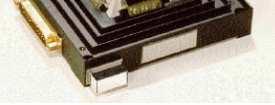
4 TNO s current portfolio Existing Products Current developments - SOTS Specials and mission specific sensors 4

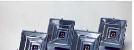
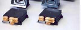
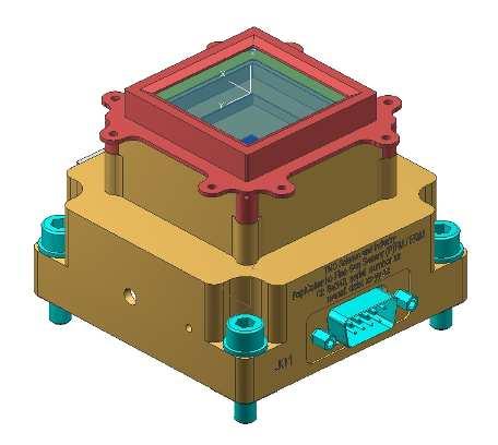
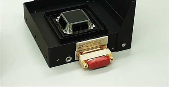
5 Start of the miniaturisation within Microned Autonomous micro-digital sunsensor Autonomous power Wireless link MEMS based 5


6 Main deliverable APS + chip Single chip sunsensor Optimised for low power TSMC 0.18 micron process Last spin-out 5 th May Chips received 23 th of june Standard design library Several circuit design modifications to avoid SEL and SEU related issues. 6


7 Key personel Albert Theuwissen Ning Xie 7


8 Key personel Murat Durkut Johan Leijtens Henk Hakkesteegt Henk Jansen 8
9 Total dose radiation tolerance 1, micron CMOS TSMC 0,9 0,8 Pixels tested up to 100 krad 0,7 0,6 No significant impact observed 0,5 0,4 Using DARE library would 0,3 0,2 increase power consumption by 0,1 0,0 factor of 2 Low power was the main requirement 20krad is sufficient for majority of applications For small systems extra shielding has less impact Quantum Efficiency P in n e d P h o to d io d e a re a /P ix e l: 5 3 (µ m 2 ) P ix e l N u m b e r: T o ta l P in n e d P h o to d io d e A re a : (µ m 2 ) In te g ra tio n T im e : 0,0 3 (s e c ) B e fo r e R a d ia tio n 8 6 k ra d k r a d W a v e le n g th (n m ) No DARE library was used 9
10 Radiation tolerance tested with gated pixel total ionizing dose (TID) level of 31krad, 86krad, 106krad, 109krad and 137krad with an average energy of 46.2keV No significant decrease in quantum efficiency No appreciable increase in dark current for 30krad Number of Pixels B e fo re R a d ia tio n 3 1 k ra d k ra d T G T ra n s is to r is o ff Ref: D a rk R a n d o m N o is e (D N ) 10
11 Increased darkcurrent not significant. Significantly lower then threshold Noise on reading less then degrees for ±47 degree system 11
12 Single Event Latch-up in CMOS Parasitic SCR (through substrate) SEL if gain >1 SEU if gain <1 Latch up can destroy the circuit N.B. Significant current can only flow if both N+ and P+ terminals are connected to low impedance, and substrate resistance is high enough 12
13 SEL hardened pixel design Winner takes all 3T pixel design Parasitic SCR through NMOS reset transistor and PMOS source follower Reduced QE due to N well for PMOS transistor n + n + n - p V N.B. Reduced QE not important for this application, because there is an abundance of light. 13
14 SEL hardened winner takes all pixel design 3.3 V All PMOS design PMOS reset transistor is not significantly reducing QE any further Extra ground connection per pixel to reduce substrate resistance.(decreases the effect of any SEU) n V n + n - p V No SCR no SEL n + p - 14
15 Ten pixel pin-hole No false detection of the sunspot due to bad pixels or SEU Replace affected pixels by the average of neighbouring pixels Automatic compensation of SEE 15
16 Single cycle acquisition through winner takes all hardware. No forbidden states in the internal state machines. Hard wired configuration straps Automatic switchback to acquisition mode at SEU Loss of accuracy for a single cycle due to SEU is the worst consequence 16
17 Conclusions Power consumption is our main driver Total dose radiation tolerance is sufficient for most sunsensor applications SEL/SEU effects are deemed more critical and tackled through several design decisions (DARE) 17
18 That s why we dare to go without DARE libraries But we don t dare to go without DARE 18 Thank you for your attention. For further information Johan Leijtens Johan.leijtens@tno.nl
Future trends in radiation hard electronics
 Future trends in radiation hard electronics F. Faccio CERN, Geneva, Switzerland Outline Radiation effects in CMOS technologies Deep submicron CMOS for radiation environments What is the future going to
EE 560 CHIP INPUT AND OUTPUT (I/0) CIRCUITS. Kenneth R. Laker, University of Pennsylvania
 CIRCUITS. Kenneth R. Laker, University of Pennsylvania") 1 EE 560 CHIP INPUT AND OUTPUT (I/0) CIRCUITS 2 -> ESD PROTECTION CIRCUITS (INPUT PADS) -> ON-CHIP CLOCK GENERATION & DISTRIBUTION -> OUTPUT PADS -> ON-CHIP NOISE DUE TO PARASITIC INDUCTANCE -> SUPER BUFFER
1 EE 560 CHIP INPUT AND OUTPUT (I/0) CIRCUITS 2 -> ESD PROTECTION CIRCUITS (INPUT PADS) -> ON-CHIP CLOCK GENERATION & DISTRIBUTION -> OUTPUT PADS -> ON-CHIP NOISE DUE TO PARASITIC INDUCTANCE -> SUPER BUFFER
Radiation Effects on Electronics. Dr. Brock J. LaMeres Associate Professor Electrical & Computer Engineering Montana State University
 Dr. Brock J. LaMeres Associate Professor Electrical & Computer Engineering Montana State University Research Statement Support the Computing Needs of Space Exploration & Science Computation Power Efficiency
The TROPOMI Telescope
 The TROPOMI Telescope Design, fabrication and test of a freeform optical system Authors: David Nijkerk Bart van Venrooy Peter van Doorn Rens Henselmans Folkert Draaisma André Hoogstrate Presented by Ad
EE371 - Advanced VLSI Circuit Design
 EE371 - Advanced VLSI Circuit Design Midterm Examination May 1999 Name: No. Points Score 1. 20 2. 24 3. 26 4. 20 TOTAL / 90 In recognition of and in the spirit of the Stanford University Honor Code, I
Your Partner in Environment Monitoring
 Your Partner in Environment Monitoring Radiation Environment in Space The ionizing radiation in space represents one of the most severe environmental loads to space hardware and can cause a large number
Lecture 16: Circuit Pitfalls
 Introduction to CMOS VLSI Design Lecture 16: Circuit Pitfalls David Harris Harvey Mudd College Spring 2004 Outline Pitfalls Detective puzzle Given circuit and symptom, diagnose cause and recommend solution
THE MICRO ADVANCED STELLAR COMPASS FOR ESA S PROBA 2 MISSION
 THE MICRO ADVANCED STELLAR COMPASS FOR ESA S PROBA 2 MISSION P.S. Jørgensen (1), J.L. Jørgensen (1), T. Denver (1), Pieter van den Braembuche (2) (1) Technical University of Denmark, Ørsted*DTU, Measurement
Lecture 7 Circuit Delay, Area and Power
 Lecture 7 Circuit Delay, Area and Power lecture notes from S. Mitra Intro VLSI System course (EE271) Introduction to VLSI Systems 1 Circuits and Delay Introduction to VLSI Systems 2 Power, Delay and Area:
EE371 - Advanced VLSI Circuit Design
 EE371 - Advanced VLSI Circuit Design Midterm Examination May 7, 2002 Name: No. Points Score 1. 18 2. 22 3. 30 TOTAL / 70 In recognition of and in the spirit of the Stanford University Honor Code, I certify
Lecture 0: Introduction
 Lecture 0: Introduction Introduction q Integrated circuits: many transistors on one chip q Very Large Scale Integration (VLSI): bucketloads! q Complementary Metal Oxide Semiconductor Fast, cheap, low power
The Devices. Digital Integrated Circuits A Design Perspective. Jan M. Rabaey Anantha Chandrakasan Borivoje Nikolic. July 30, 2002
 Digital Integrated Circuits A Design Perspective Jan M. Rabaey Anantha Chandrakasan Borivoje Nikolic The Devices July 30, 2002 Goal of this chapter Present intuitive understanding of device operation Introduction
CARNEGIE MELLON UNIVERSITY DEPARTMENT OF ELECTRICAL AND COMPUTER ENGINEERING DIGITAL INTEGRATED CIRCUITS FALL 2002
 CARNEGIE MELLON UNIVERSITY DEPARTMENT OF ELECTRICAL AND COMPUTER ENGINEERING 18-322 DIGITAL INTEGRATED CIRCUITS FALL 2002 Final Examination, Monday Dec. 16, 2002 NAME: SECTION: Time: 180 minutes Closed
Picometre metrology. The Gaia mission will create an ultra-precise three-dimensional map of about one billion stars
 Picometre metrology in space The Gaia mission will create an ultra-precise three-dimensional map of about one billion stars in our Galaxy. Part of ESA s Cosmic Vision program, the Gaia spacecraft is being
ESA Technical Development Activities An Overview
 ESA Technical Development Activities An Overview Christian Erd EJSM Instrument Workshop 18 20 January 2010 18 20 January 2010 C. Erd 1 Technology Overview A preliminary list was compiled ESA activities
Lecture 2: CMOS technology. Energy-aware computing
 Energy-Aware Computing Lecture 2: CMOS technology Basic components Transistors Two types: NMOS, PMOS Wires (interconnect) Transistors as switches Gate Drain Source NMOS: When G is @ logic 1 (actually over
LEADING THE EVOLUTION OF COMPUTE MARK KACHMAREK HPC STRATEGIC PLANNING MANAGER APRIL 17, 2018
 LEADING THE EVOLUTION OF COMPUTE MARK KACHMAREK HPC STRATEGIC PLANNING MANAGER APRIL 17, 2018 INTEL S RESEARCH EFFORTS COMPONENTS RESEARCH INTEL LABS ENABLING MOORE S LAW DEVELOPING NOVEL INTEGRATION ENABLING
EE115C Winter 2017 Digital Electronic Circuits. Lecture 3: MOS RC Model, CMOS Manufacturing
 EE115C Winter 2017 Digital Electronic Circuits Lecture 3: MOS RC Model, CMOS Manufacturing Agenda MOS Transistor: RC Model (pp. 104-113) S R on D CMOS Manufacturing Process (pp. 36-46) S S C GS G G C GD
ECE 342 Electronic Circuits. 3. MOS Transistors
 ECE 342 Electronic Circuits 3. MOS Transistors Jose E. Schutt-Aine Electrical & Computer Engineering University of Illinois jschutt@emlab.uiuc.edu 1 NMOS Transistor Typically L = 0.1 to 3 m, W = 0.2 to
Digital Integrated Circuits A Design Perspective. Jan M. Rabaey Anantha Chandrakasan Borivoje Nikolic. The Devices. July 30, Devices.
 Digital Integrated Circuits A Design Perspective Jan M. Rabaey Anantha Chandrakasan Borivoje Nikolic The July 30, 2002 1 Goal of this chapter Present intuitive understanding of device operation Introduction
Features OUT A NC 27 NC IN 8A IN 16 IN 7A IN 15 IN 6A IN 14 IN 5A IN 13 IN 4A IN 12 IN 3A IN 11 IN 2A IN 10 IN 1A IN 9 ENABLE GND ADDRESS A0 V REF
 DATASHEET HS-0RH, HS-0RH Radiation Hardened Single /Differential Channel CMOS Analog Multiplexers with Active Overvoltage rotection F Rev..00 The HS-0RH and HS-0RH are radiation hardened analog multiplexers
Sensors: a) Gyroscope. Micro Electro-Mechanical (MEM) Gyroscopes: (MEM) Gyroscopes. Needs:
 Gyroscope. Micro Electro-Mechanical (MEM) Gyroscopes: (MEM) Gyroscopes. Needs:") Sensors: Needs: Data redundancy Data for both situations: eclipse and sun Question of sampling frequency Location and size/weight Ability to resist to environment Low consumption Low price a) Gyroscope
Sensors: Needs: Data redundancy Data for both situations: eclipse and sun Question of sampling frequency Location and size/weight Ability to resist to environment Low consumption Low price a) Gyroscope
Lecture 16: Circuit Pitfalls
 Lecture 16: Circuit Pitfalls Outline Variation Noise Budgets Reliability Circuit Pitfalls 2 Variation Process Threshold Channel length Interconnect dimensions Environment Voltage Temperature Aging / Wearout
UNIVERSITY OF CALIFORNIA, BERKELEY College of Engineering Department of Electrical Engineering and Computer Sciences
 UNIVERSITY OF CALIFORNIA, BERKELEY College of Engineering Department of Electrical Engineering and Computer Sciences Elad Alon Homework #9 EECS141 PROBLEM 1: TIMING Consider the simple state machine shown
Interconnect (2) Buffering Techniques.Transmission Lines. Lecture Fall 2003
 Buffering Techniques.Transmission Lines. Lecture Fall 2003") Interconnect (2) Buffering Techniques.Transmission Lines Lecture 12 18-322 Fall 2003 A few announcements Partners Lab Due Times Midterm 1 is nearly here Date: 10/14/02, time: 3:00-4:20PM, place: in class
Interconnect (2) Buffering Techniques.Transmission Lines Lecture 12 18-322 Fall 2003 A few announcements Partners Lab Due Times Midterm 1 is nearly here Date: 10/14/02, time: 3:00-4:20PM, place: in class
L ECE 4211 UConn F. Jain Scaling Laws for NanoFETs Chapter 10 Logic Gate Scaling
 L13 04202017 ECE 4211 UConn F. Jain Scaling Laws for NanoFETs Chapter 10 Logic Gate Scaling Scaling laws: Generalized scaling (GS) p. 610 Design steps p.613 Nanotransistor issues (page 626) Degradation
DISTRIBUTION LIST. Others original copies Name amount. Lens Research & Development 1x Uittenhout, J.M.M. 1x DOCUMENT CHANGE RECORD
 2 of 15 DISTRIBUTION LIST Others original copies Name amount Lens Research & Development 1x Uittenhout, J.M.M. 1x DOCUMENT CHANGE RECORD Issue Date Total pages Pages affected Brief description of change
Lecture 6: Time-Dependent Behaviour of Digital Circuits
 Lecture 6: Time-Dependent Behaviour of Digital Circuits Two rather different quasi-physical models of an inverter gate were discussed in the previous lecture. The first one was a simple delay model. This
Interconnects. Wire Resistance Wire Capacitance Wire RC Delay Crosstalk Wire Engineering Repeaters. ECE 261 James Morizio 1
 Interconnects Wire Resistance Wire Capacitance Wire RC Delay Crosstalk Wire Engineering Repeaters ECE 261 James Morizio 1 Introduction Chips are mostly made of wires called interconnect In stick diagram,
S-1000 Series ULTRA-SMALL PACKAGE HIGH-PRECISION VOLTAGE DETECTOR. Features. Applications. Packages. Seiko Instruments Inc. 1.
 S-1000 Series www.sii-ic.com ULTRA-SMALL PACKAGE HIGH-PRECISION VOLTAGE DETECTOR Seiko Instruments Inc., 2004-2015 Rev.3.1_00 The S-1000 series is a series of high-precision voltage detectors developed
Very Large Scale Integration (VLSI)
") Very Large Scale Integration (VLSI) Lecture 4 Dr. Ahmed H. Madian Ah_madian@hotmail.com Dr. Ahmed H. Madian-VLSI Contents Delay estimation Simple RC model Penfield-Rubenstein Model Logical effort Delay
Very Large Scale Integration (VLSI) Lecture 4 Dr. Ahmed H. Madian Ah_madian@hotmail.com Dr. Ahmed H. Madian-VLSI Contents Delay estimation Simple RC model Penfield-Rubenstein Model Logical effort Delay
CMOS Inverter (static view)
") Review: Design Abstraction Levels SYSTEM CMOS Inverter (static view) + MODULE GATE [Adapted from Chapter 5. 5.3 CIRCUIT of G DEVICE Rabaey s Digital Integrated Circuits,, J. Rabaey et al.] S D Review:
Review: Design Abstraction Levels SYSTEM CMOS Inverter (static view) + MODULE GATE [Adapted from Chapter 5. 5.3 CIRCUIT of G DEVICE Rabaey s Digital Integrated Circuits,, J. Rabaey et al.] S D Review:
DATASHEET HS-0548RH, HS-0549RH. Features. Applications. Pinouts. Ordering Information
 DATASHEET HS-0RH, HS-0RH Radiation Hardened Single /Differential Channel CMOS Analog Multiplexers with Active Overvoltage rotection F Rev.00 August 00 The HS-0RH and HS-0RH are radiation hardened analog
Digital Electronics Part II - Circuits
 Digital Electronics Part - Circuits Dr.. J. Wassell Gates from Transistors ntroduction Logic circuits are non-linear, consequently we will introduce a graphical technique for analysing such circuits The
80386DX. 32-Bit Microprocessor FEATURES: DESCRIPTION: Logic Diagram
 32-Bit Microprocessor 21 1 22 1 2 10 3 103 FEATURES: 32-Bit microprocessor RAD-PAK radiation-hardened agait natural space radiation Total dose hardness: - >100 Krad (Si), dependent upon space mission Single
CSE241 VLSI Digital Circuits Winter Lecture 07: Timing II
 CSE241 VLSI Digital Circuits Winter 2003 Lecture 07: Timing II CSE241 L3 ASICs.1 Delay Calculation Cell Fall Cap\Tr 0.05 0.2 0.5 0.01 0.02 0.16 0.30 0.5 2.0 0.04 0.32 0.178 0.08 0.64 0.60 1.20 0.1ns 0.147ns
Display counter electromechanical
 Micro Display counter K 04... K 07, shock resistant 4-, 5-, 6- and 7 digit Micro adding counter High shock resistance Low power consumption; suitable for battery consumption small dimensions Large optical
CMPEN 411 VLSI Digital Circuits. Lecture 03: MOS Transistor
 CMPEN 411 VLSI Digital Circuits Lecture 03: MOS Transistor Kyusun Choi [Adapted from Rabaey s Digital Integrated Circuits, Second Edition, 2003 J. Rabaey, A. Chandrakasan, B. Nikolic] CMPEN 411 L03 S.1
A Stellar Gyroscope for CubeSat Attitude Determination
 A Stellar Gyroscope for CubeSat Attitude Determination Samir A. Rawashdeh and James E. Lumpp, Jr. Space Systems Laboratory University of Kentucky James Barrington-Brown and Massimiliano Pastena SSBV Space
Development of a Radiation Hard CMOS Monolithic Pixel Sensor
 Development of a Radiation Hard CMOS Monolithic Pixel Sensor M. Battaglia 1,2, D. Bisello 3, D. Contarato 2, P. Denes 2, D. Doering 2, P. Giubilato 2,3, T.S. Kim 2, Z. Lee 2, S. Mattiazzo 3, V. Radmilovic
Lecture 8. Detectors for Ionizing Particles
 Lecture 8 Detectors for Ionizing Particles Content Introduction Overview of detector systems Sources of radiation Radioactive decay Cosmic Radiation Accelerators Interaction of Radiation with Matter General
EE141Microelettronica. CMOS Logic
 Microelettronica CMOS Logic CMOS logic Power consumption in CMOS logic gates Where Does Power Go in CMOS? Dynamic Power Consumption Charging and Discharging Capacitors Short Circuit Currents Short Circuit
Spiral 2 7. Capacitance, Delay and Sizing. Mark Redekopp
 2-7.1 Spiral 2 7 Capacitance, Delay and Sizing Mark Redekopp 2-7.2 Learning Outcomes I understand the sources of capacitance in CMOS circuits I understand how delay scales with resistance, capacitance
The Devices: MOS Transistors
 The Devices: MOS Transistors References: Semiconductor Device Fundamentals, R. F. Pierret, Addison-Wesley Digital Integrated Circuits: A Design Perspective, J. Rabaey et.al. Prentice Hall NMOS Transistor
Realization of 2:4 reversible decoder and its applications
 Realization of 2:4 reversible decoder and its applications Neeta Pandey n66pandey@rediffmail.com Nalin Dadhich dadhich.nalin@gmail.com Mohd. Zubair Talha zubair.talha2010@gmail.com Abstract In this paper
CMPEN 411 VLSI Digital Circuits Spring 2011 Lecture 07: Pass Transistor Logic
 CMPEN 411 VLSI Digital Circuits Spring 2011 Lecture 07: Pass Transistor Logic [dapted from Rabaey s Digital Integrated Circuits, Second Edition, 2003 J. Rabaey,. Chandrakasan,. Nikolic] Sp11 CMPEN 411
Transistor Sizing for Radiation Hardening
 Transistor Sizing for Radiation Hardening Qug Zhou and Kartik Mohanram Department of Electrical and Computer Engineering Rice University, Houston, TX 775 E-mail: {qug, kmram}@rice.edu Abstract This paper
Small Satellite Laser Comm Pointing
 Small Satellite Laser Comm Pointing Darren Rowen July 11, 2016 2016 The Aerospace Corporation Agenda Optical Ground Station Tracking Demo of Cubesat Laser OCSD-B/C Design & Configuration OCSD-A Star Tracker
Lecture 6 Power Zhuo Feng. Z. Feng MTU EE4800 CMOS Digital IC Design & Analysis 2010
 EE4800 CMOS Digital IC Design & Analysis Lecture 6 Power Zhuo Feng 6.1 Outline Power and Energy Dynamic Power Static Power 6.2 Power and Energy Power is drawn from a voltage source attached to the V DD
CMOS Digital Integrated Circuits Lec 13 Semiconductor Memories
 Lec 13 Semiconductor Memories 1 Semiconductor Memory Types Semiconductor Memories Read/Write (R/W) Memory or Random Access Memory (RAM) Read-Only Memory (ROM) Dynamic RAM (DRAM) Static RAM (SRAM) 1. Mask
VLSI Design, Fall Logical Effort. Jacob Abraham
 6. Logical Effort 6. Logical Effort Jacob Abraham Department of Electrical and Computer Engineering The University of Texas at Austin VLSI Design Fall 207 September 20, 207 ECE Department, University of
MODULE 5 Chapter 7. Clocked Storage Elements
 MODULE 5 Chapter 7 Clocked Storage Elements 3/9/2015 1 Outline Background Clocked Storage Elements Timing, terminology, classification Static CSEs Latches Registers Dynamic CSEs Latches Registers 3/9/2015
ELEN0037 Microelectronic IC Design. Prof. Dr. Michael Kraft
 ELEN0037 Microelectronic IC Design Prof. Dr. Michael Kraft Lecture 2: Technological Aspects Technology Passive components Active components CMOS Process Basic Layout Scaling CMOS Technology Integrated
Centre for Electronic Imaging
 Centre for Electronic Imaging Calibration plans for the Soft X-ray Imager s CCDs on SMILE Open University: George Randall, Matthew Soman, David Hall, Andrew Holland, Ross Burgon, Jonathan Keelan, Thomas
Semiconductor memories
 Semiconductor memories Semiconductor Memories Data in Write Memory cell Read Data out Some design issues : How many cells? Function? Power consuption? Access type? How fast are read/write operations? Semiconductor
THE INVERTER. Inverter
 THE INVERTER DIGITAL GATES Fundamental Parameters Functionality Reliability, Robustness Area Performance» Speed (delay)» Power Consumption» Energy Noise in Digital Integrated Circuits v(t) V DD i(t) (a)
Interconnects. Introduction
 Interconnects Wire Resistance Wire Capacitance Wire RC Delay Crosstalk Wire Engineering Repeaters ECE 261 Krish Chakrabarty 1 Introduction Chips are mostly made of ires called interconnect In stick diagram,
5.0 CMOS Inverter. W.Kucewicz VLSICirciuit Design 1
 5.0 CMOS Inverter W.Kucewicz VLSICirciuit Design 1 Properties Switching Threshold Dynamic Behaviour Capacitance Propagation Delay nmos/pmos Ratio Power Consumption Contents W.Kucewicz VLSICirciuit Design
Cosmic Ray Effects on Micro- Electronics (CRÈME) Tools Brian Sierawski 2017 SEESAW
 Tools Brian Sierawski 2017 SEESAW") Cosmic Ray Effects on Micro- Electronics (CRÈME) Tools Brian Sierawski 2017 SEESAW CRÈME Website Vanderbilt Engineering ISDE hosts the CRÈME tool suite for predicting on-orbit error rates and proton total
Cosmic Ray Effects on Micro- Electronics (CRÈME) Tools Brian Sierawski 2017 SEESAW CRÈME Website Vanderbilt Engineering ISDE hosts the CRÈME tool suite for predicting on-orbit error rates and proton total
Radiation damage considerations in accelerator beam environments
 Radiation damage considerations in accelerator beam environments DAVID V WEBB PhD (ret d) Ex-Aust. Radiation Protection & Nuclear Safety Agency Yallambie, Victoria, Australia Overview The impact of radiation
Single Event Radiation Test Report. Microsemi LX Analog Input RAD Tolerant Telemetry Controller
 Single Event Radiation Test Report Microsemi LX7730 64 Analog Input RAD Tolerant Telemetry Controller Doc. N :TDRS-0020-4 Page 1/33 TABLE OF CONTENT 1. PURPOSE AND SCOPE... 3 2. APPLICABLE DOCUMENT...
Homework Assignment #5 EE 477 Spring 2017 Professor Parker
 Homework Assignment #5 EE 477 Spring 2017 Professor Parker Question 1: (15%) Compute the worst-case rising and falling RC time constants at point B of the circuit below using the Elmore delay method. Assume
VORAGO TECHNOLOGIES. Cost-effective rad-hard MCU Solution for SmallSats Ross Bannatyne, VORAGO Technologies
 VORAGO TECHNOLOGIES Cost-effective rad-hard MCU Solution for SmallSats Ross Bannatyne, VORAGO Technologies V O R A G O Te c h n o l o g i e s Privately held fabless semiconductor company headquartered
Grasping The Deep Sub-Micron Challenge in POWERFUL Integrated Circuits
 E = B; H = J + D D = ρ ; B = 0 D = ρ ; B = 0 Yehia Massoud ECE Department Rice University Grasping The Deep Sub-Micron Challenge in POWERFUL Integrated Circuits ECE Affiliates 10/8/2003 Background: Integrated
S-5743 A Series 125 C OPERATION HIGH-WITHSTAND VOLTAGE HIGH-SPEED BIPOLAR HALL EFFECT LATCH IC. Features. Applications. Package.
 www.ablicinc.com S-5743 A Series 125 C OPERATION HIGH-WITHSTAND VOLTAGE HIGH-SPEED BIPOLAR HALL EFFECT LATCH IC ABLIC Inc., 2015-2017 Rev.1.1_02 This IC, developed by CMOS technology, is a high-accuracy
DOE SBIR & STTR FY 2019 Phase 1, Release 1 Topics
 Source: InternetCoast BUSINESS OPPORTUNITIES web page>>> Letter of Intent Deadline: September 4, 2018 Application Deadline: October 15, 2018 Download Solicitation Topic Details>>> 1. TECHNOLOGIES FOR MANAGING
Estec final presentation days 2018
 Estec final presentation days 2018 Background VESPER Facility Conclusion & Outlook Jovian environment Radiation Effects VESPER history VESPER status Overview Experimental Results External Campaign Summary
University of BRISTOL. Department of Physics. Final year project. MAPS (Monolithic Active Pixel Sensors) Degree: Physics MSci (F303) May 10, 2011
 Degree: Physics MSci (F303) May 10, 2011") University of BRISTOL Department of Physics Final year project MAPS (Monolithic Active Pixel Sensors) Author: Richard Webster Degree: Physics MSci (F303) Supervisors: Dr. Joel Goldstein Project Number:
University of BRISTOL Department of Physics Final year project MAPS (Monolithic Active Pixel Sensors) Author: Richard Webster Degree: Physics MSci (F303) Supervisors: Dr. Joel Goldstein Project Number:
EE410 vs. Advanced CMOS Structures
 EE410 vs. Advanced CMOS Structures Prof. Krishna S Department of Electrical Engineering S 1 EE410 CMOS Structure P + poly-si N + poly-si Al/Si alloy LPCVD PSG P + P + N + N + PMOS N-substrate NMOS P-well
CMOS INVERTER. Last Lecture. Metrics for qualifying digital circuits. »Cost» Reliability» Speed (delay)»performance
»performance") CMOS INVERTER Last Lecture Metrics for qualifying digital circuits»cost» Reliability» Speed (delay)»performance 1 Today s lecture The CMOS inverter at a glance An MOS transistor model for manual analysis
CMOS INVERTER Last Lecture Metrics for qualifying digital circuits»cost» Reliability» Speed (delay)»performance 1 Today s lecture The CMOS inverter at a glance An MOS transistor model for manual analysis
Heavy ion radiation damage simulations for CMOS image sensors
 Heavy ion radiation damage simulations for CMOS image sensors Henok Mebrahtu a, Wei Gao a, Paul J. Thomas b*, William E. Kieser c, Richard I. Hornsey a a Department of Computer Science, York University,
ESE570 Spring University of Pennsylvania Department of Electrical and System Engineering Digital Integrated Cicruits AND VLSI Fundamentals
 University of Pennsylvania Department of Electrical and System Engineering Digital Integrated Cicruits AND VLSI Fundamentals ESE570, Spring 2018 Final Monday, Apr 0 5 Problems with point weightings shown.
Single-photon and two-photon absorption induced charge model calibration
 Single-photon and two-photon absorption induced charge model calibration Vincent Pouget IES CNRS, University of Montpellier Motivation Follow-up of RADLAS2013 presentation on TPA modeling Many use cases
Calibration of Ocean Colour Sensors
 Dr. A. Neumann German Aerospace Centre DLR Remote Sensing Technology Institute Marine Remote Sensing What is Calibration, why do we need it? Sensor Components Definition of Terms Calibration Standards
ESE 570: Digital Integrated Circuits and VLSI Fundamentals
 ESE 570: Digital Integrated Circuits and VLSI Fundamentals Lec 23: April 13, 2017 Variation; I/O Circuits, Inductive Noise Lecture Outline! Design Quality " Variation! Packaging! Variation and Testing!
CMPEN 411 VLSI Digital Circuits. Lecture 04: CMOS Inverter (static view)
") CMPEN 411 VLSI Digital Circuits Lecture 04: CMOS Inverter (static view) Kyusun Choi [Adapted from Rabaey s Digital Integrated Circuits, Second Edition, 2003 J. Rabaey, A. Chandrakasan, B. Nikolic] CMPEN
CMPEN 411 VLSI Digital Circuits Lecture 04: CMOS Inverter (static view) Kyusun Choi [Adapted from Rabaey s Digital Integrated Circuits, Second Edition, 2003 J. Rabaey, A. Chandrakasan, B. Nikolic] CMPEN
Detector R&D in KAPAC
 Detector R&D in KAPAC Hiroyasu Tajima Stanford Linear Accelerator Center Kavli Institute for Particle Astrophysics and Cosmology Outline Compton Camera SOI detector Scintillator Polarimeter Cherenkov Camera
A final review session will be offered on Thursday, May 10 from 10AM to 12noon in 521 Cory (the Hogan Room).
.") A final review session will be offered on Thursday, May 10 from 10AM to 12noon in 521 Cory (the Hogan Room). The Final Exam will take place from 12:30PM to 3:30PM on Saturday May 12 in 60 Evans.» All of
A final review session will be offered on Thursday, May 10 from 10AM to 12noon in 521 Cory (the Hogan Room). The Final Exam will take place from 12:30PM to 3:30PM on Saturday May 12 in 60 Evans.» All of
S-57P1 S Series FOR AUTOMOTIVE 150 C OPERATION HIGH-WITHSTAND VOLTAGE HIGH-SPEED BIPOLAR HALL EFFECT LATCH IC. Features. Applications.
 www.ablicinc.com FOR AUTOMOTIVE 150 C OPERATION HIGH-WITHSTAND VOLTAGE HIGH-SPEED BIPOLAR HALL EFFECT LATCH IC ABLIC Inc., 2015-2017 This IC, developed by CMOS technology, is a high-accuracy Hall effect
Low Power VLSI Circuits and Systems Prof. Ajit Pal Department of Computer Science and Engineering Indian Institute of Technology, Kharagpur
 Low Power VLSI Circuits and Systems Prof. Ajit Pal Department of Computer Science and Engineering Indian Institute of Technology, Kharagpur Lecture No. # 08 MOS Inverters - III Hello, and welcome to today
HN27C4096G/CC Series. Ordering Information. Features word 16-bit CMOS UV Erasable and Programmable ROM
 262144-word 16-bit CMOS UV Erasable and Programmable ROM The Hitachi HN27C4096G/CC is a 4-Mbit ultraviolet erasable and electrically programmable ROM, featuring high speed and low power dissipation. Fabricated
The Devices. Digital Integrated Circuits A Design Perspective. Jan M. Rabaey Anantha Chandrakasan Borivoje Nikolic. July 30, 2002
 igital Integrated Circuits A esign Perspective Jan M. Rabaey Anantha Chandrakasan Borivoje Nikolic The evices July 30, 2002 Goal of this chapter Present intuitive understanding of device operation Introduction
CPE/EE 427, CPE 527 VLSI Design I Delay Estimation. Department of Electrical and Computer Engineering University of Alabama in Huntsville
 CPE/EE 47, CPE 57 VLSI Design I Delay Estimation Department of Electrical and Computer Engineering University of labama in Huntsville leksandar Milenkovic ( www.ece.uah.edu/~milenka ) Review: CMOS Circuit
ENGR890 Digital VLSI Design Fall Lecture 4: CMOS Inverter (static view)
") ENGR89 Digital VLSI Design Fall 5 Lecture 4: CMOS Inverter (static view) [Adapted from Chapter 5 of Digital Integrated Circuits, 3, J. Rabaey et al.] [Also borrowed from Vijay Narayanan and Mary Jane Irwin]
ENGR89 Digital VLSI Design Fall 5 Lecture 4: CMOS Inverter (static view) [Adapted from Chapter 5 of Digital Integrated Circuits, 3, J. Rabaey et al.] [Also borrowed from Vijay Narayanan and Mary Jane Irwin]
Chapter 2. Design and Fabrication of VLSI Devices
 Chapter 2 Design and Fabrication of VLSI Devices Jason Cong 1 Design and Fabrication of VLSI Devices Objectives: To study the materials used in fabrication of VLSI devices. To study the structure of devices
Digital Integrated Circuits A Design Perspective
 Semiconductor Memories Adapted from Chapter 12 of Digital Integrated Circuits A Design Perspective Jan M. Rabaey et al. Copyright 2003 Prentice Hall/Pearson Outline Memory Classification Memory Architectures
CMOS Transistors, Gates, and Wires
 CMOS Transistors, Gates, and Wires Should the hardware abstraction layers make today s lecture irrelevant? pplication R P C W / R W C W / 6.375 Complex Digital Systems Christopher atten February 5, 006
Preamplifier in 0.5µm CMOS
 A 2.125 Gbaud 1.6kΩ Transimpedance Preamplifier in 0.5µm CMOS Sunderarajan S. Mohan Thomas H. Lee Center for Integrated Systems Stanford University OUTLINE Motivation Shunt-peaked Amplifier Inductor Modeling
Introduction to CMOS VLSI Design Lecture 1: Introduction
 Introduction to CMOS VLSI Design Lecture 1: Introduction David Harris, Harvey Mudd College Kartik Mohanram and Steven Levitan University of Pittsburgh Introduction Integrated circuits: many transistors
ECE Branch GATE Paper The order of the differential equation + + = is (A) 1 (B) 2
 1 (B) 2") Question 1 Question 20 carry one mark each. 1. The order of the differential equation + + = is (A) 1 (B) 2 (C) 3 (D) 4 2. The Fourier series of a real periodic function has only P. Cosine terms if it is
Question 1 Question 20 carry one mark each. 1. The order of the differential equation + + = is (A) 1 (B) 2 (C) 3 (D) 4 2. The Fourier series of a real periodic function has only P. Cosine terms if it is
MTJ-Based Nonvolatile Logic-in-Memory Architecture and Its Application
 2011 11th Non-Volatile Memory Technology Symposium @ Shanghai, China, Nov. 9, 20112 MTJ-Based Nonvolatile Logic-in-Memory Architecture and Its Application Takahiro Hanyu 1,3, S. Matsunaga 1, D. Suzuki
S-57M1 Series HIGH-SPEED BIPOLAR HALL EFFECT LATCH. Features. Applications. Package. ABLIC Inc., Rev.1.
 www.ablic.com www.ablicinc.com HIGH-SPEED BIPOLAR HALL EFFECT LATCH ABLIC Inc., 2011-2013 Rev.1.2_02 The, developed by CMOS technology, is a high-accuracy Hall IC that operates with a high-sensitivity,
Introduction. Simulation methodology. Simulation results
 Introduction Simulation methodology Simulation results Conclusion and Perspectives Introduction Simulation methodology Simulation results Conclusion and Perspectives Radiation induced particles Solar Flare
and V DS V GS V T (the saturation region) I DS = k 2 (V GS V T )2 (1+ V DS )
 I DS = k 2 (V GS V T )2 (1+ V DS )") ECE 4420 Spring 2005 Page 1 FINAL EXAMINATION NAME SCORE /100 Problem 1O 2 3 4 5 6 7 Sum Points INSTRUCTIONS: This exam is closed book. You are permitted four sheets of notes (three of which are your sheets
ECE 4420 Spring 2005 Page 1 FINAL EXAMINATION NAME SCORE /100 Problem 1O 2 3 4 5 6 7 Sum Points INSTRUCTIONS: This exam is closed book. You are permitted four sheets of notes (three of which are your sheets
The Devices. Jan M. Rabaey
 The Devices Jan M. Rabaey Goal of this chapter Present intuitive understanding of device operation Introduction of basic device equations Introduction of models for manual analysis Introduction of models
Digital Integrated Circuits A Design Perspective
 igital Integrated Circuits esign Perspective esigning Combinational Logic Circuits 1 Combinational vs. Sequential Logic In Combinational Logic Circuit Out In Combinational Logic Circuit Out State Combinational
EECS 151/251A Homework 5
 EECS 151/251A Homework 5 Due Monday, March 5 th, 2018 Problem 1: Timing The data-path shown below is used in a simple processor. clk rd1 rd2 0 wr regfile 1 0 ALU REG 1 The elements used in the design have
Lecture Notes 2 Charge-Coupled Devices (CCDs) Part I. Basic CCD Operation CCD Image Sensor Architectures Static and Dynamic Analysis
 Part I. Basic CCD Operation CCD Image Sensor Architectures Static and Dynamic Analysis") Lecture Notes 2 Charge-Coupled Devices (CCDs) Part I Basic CCD Operation CCD Image Sensor Architectures Static and Dynamic Analysis Charge Well Capacity Buried channel CCD Transfer Efficiency Readout Speed
Lecture Notes 2 Charge-Coupled Devices (CCDs) Part I Basic CCD Operation CCD Image Sensor Architectures Static and Dynamic Analysis Charge Well Capacity Buried channel CCD Transfer Efficiency Readout Speed
Designing Information Devices and Systems II Spring 2018 J. Roychowdhury and M. Maharbiz Discussion 1A
 EEC 16B esigning Information evices and ystems II pring 2018 J. Roychowdhury and M. Maharbiz iscussion 1A 1 igit Bases (N) p is used to indicate that the number N is expressed in base p. For example, (N)
Lunar Reconnaissance Orbiter Project. Radiation Requirements. August 5, 2005
 Effective Date: November 7, 2005 Expiration Date: November 7, 2010 Lunar Reconnaissance Orbiter Project Radiation Requirements August 5, 2005 LRO GSFC CMO November 7, 2005 RELEASED Goddard Space Flight