B12: Semiconductor Devices
|
|
|
- Kristian Houston
- 6 years ago
- Views:
Transcription
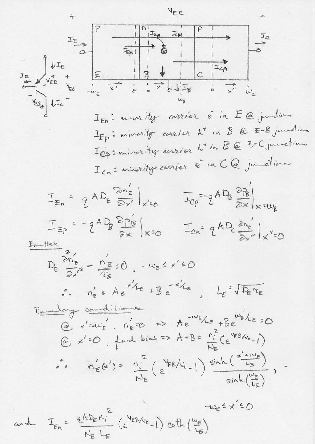
1 B12: Semiconductor Devices Example Sheet 2: Solutions Question 1 To get from eq. (5.70) of the notes to the expression given in the examples sheet, we simply invoke the relations n 0 p 0, n 0 n 0. In this case, we have that D 0 D p and µ 0 µ p. Furthermore, the analysis of bandto-band recombination yielded the expression R = p 0 / p. The stated result follows. For the second part of the question, it is stated that E = 0 2 p 0 /@x 2 = 0. The ambipolar transport equation is thus given = G p0 p. The complementary solution to this di erential equation can be found by setting G = 0, which yields p 0 c(t) =Ae t/ p for some constant A. Considering the steady-state (t!1), the di erential equation becomes 0=G p0 p ) p 0 (1) =G p. Since p 0 c(1) = 0, the steady-state solution is simply the particular solution. Putting it all together yields p 0 (t) =G p + p 0 c(t). Invoking the initial condition p 0 (0) = 0 reveals that A = p 0 (t) =G p (1 e t/ p ), t 0. G p, so the total solution is The excess minority carrier hole concentration increases monotonically in a uniform manner across the substrate according to the product of the rate of carrier generation and the mean time to recombination, approaching this product in the steady-state. For the final part of the question, one can simply di erentiate the given expression a few times with respect to the position and time variables to show that the ambipolar transport equation, with G = 0, is satisfied. This solution suggests that, initially, there is a large concentration of carriers local to x = 0. As time progresses, the excess holes drift en masse in the positive x direction and simultaneously di use symmetrically about 1
2 the point x = µ p Et in a Gaussian-like manner (see Figure 1). As t grows large, the excess carrier concentration tends to zero in a spatially uniform manner, provided the substrate has infinite length. Although not treated in this question, it is interesting to note that in a substrate of finite length, a rather complicated behaviour of the excess minority carrier hole concentration would be observed, which would arise from the drift/di usion process described above, but where carriers would collect at the right-hand boundary (say, x = `) whilst simultaneously recombining at the rate p 0 (`)/ p Figure 1: p 0 (x, t) vsx for µ p Et =0.1, 0.5, 1.0. Question 2 The energy band diagram for a zero bias is shown in Figure 2. In a pn junction under zero bias, the Fermi energy is constant, with the valence band edge situated close to the Fermi energy in the p region and the conduction band edge situated close to the Fermi energy in the n region. The intrinsic Fermi level lies roughly at the mid-gap point across the device, and thus it is position dependent. Di usion causes majority carrier holes in the p region to move into the n region, and majority carrier electrons in the n region move into the p region. This process creates a charge separation, which results in an induced electric field oriented from the n region toward the p region (from positive to negative). Eventually, this field perfectly balances the di usion action, and equilibrium is reached. The field e ectively prevents holes in the p region from di using across the metallurgical junction. Equivalently, it pushes electrons in the n region away from the junction as well. This yields a space charge or depletion region around the junction, which is largely devoid of carriers. This region is, however, locally charged since there is a fixed lattice of charged impurity atoms (positively charged donor ions in the n region and negatively charged acceptor ions in the p region). The potential di erence that is induced across the depletion region is known as the built-in potential and is denoted by V bi in the figure. This potential is equal to the sum of the di erences in the Fermi and 2
3 intrinsic Fermi levels in the n and p regions. p metallurgical!! n! junction! E c! ev bi! E Fi! ev Fp! E F! E v! ev Fn! Figure 2: Energy band diagram for a pn junction with no bias. Figure 3 shows the energy band diagram for a device in forward bias mode. The applied bias counteracts the induced electric field (equivalently, the built-in potential). Majority carrier electrons in the n region situated beyond the depletion region require less energy to overcome the potential barrier between the n and p regions, and thus carriers move more freely between the regions. Current flows from the p to the n region. E c! ev Total! E Fi! E Fp! ev Fp! ev Fn! E Fn! ev A! E v! Figure 3: Energy band diagram for a pn junction with a forward bias. Carrier transport describes current flow in a pn junction. Transport is related to the excess minority carrier concentrations in the p and n regions. Carrier concentrations are derived by integrating the product of the density of states function and the Fermi-Dirac probability function across all energy values in a given band. This yields an expression that is proportional to an exponential with an argument that quantifies the potential di erence between a given band edge and the Fermi level. When a bias is applied, the potential associated with the bias is incorporated into the argument of the exponential by solving the ambipolar transport equation. To obtain the current through the device, 3

4 the di usion equations are solved, which require one to di erentiate the excess carrier concentration functions. Since these are exponentials, their form is retained through the di erentiation and the total current will have an exponential form. Question 3 For a one-sided junction with N a N d, the regions and di usion currents resemble those shown in Figure 4. Notice the small space charge width in the p-type material and the very low excess minority carrier electron di usion current in the p region. The ideal diode equation is derived in exactly the same way as in the notes. We simply note that, due to the relation N a N d,wehave I AJ p (x n )= qad pn 2 i VA exp 1. L p N d V t Applied electric field! p! J p! n! J n! Induced electric field! Figure 4: One-sided junction diagram with di usion currents. Question 4 The correct answer should be centred around the discussion given in sections 7.1 and 7.2 of the notes. Specifically, it is important to note that photodiodes are reverse biased so that, when a photon generates carriers in the depletion region, the current resulting from the carriers moving in opposite directions can be easily detected. It is also important to note that the choice of semiconductor will dictate what wavelength of light can be detected, with the band gap of the semiconductor adhering to E g apple 1.24 ev 4
5 with being measured in microns. The main things to note in relation to the generation of light are that the recombination process results in photon emission in direct band gap semiconductors, but phonons are typically emitted in indirect band gap materials since a change in momentum is required for an electron to jump from the bottom of the conduction band to the top of the valence band. It is also important to note that Si is an indirect band gap semiconductor, whilst GaAs is a direct band gap semiconductor. For this reason, GaAs is a very important semiconductor for optical applications. Question 5 (See appended hand-written work.) Question 6 We adopt the setup depicted in Figure 5. Firstly, we note that the cuto frequency is defined as f T = 1 2 ec where ec b + d = w2 B + w BC. 2D B v s From the figure, we can rewrite this as ec w2 B 2D B + 2x 0 v s 2w B v s. To maximise the cuto frequency, we find the base width that yields the minimum of the emitter-collector delay. This gives and, using the figure, we have w B = 2D B v s w BC =2 x 0 2D B. v s These optima yield the minimum value for the emitter-collector delay: ec 2 D B x 0. v s v s We immediately see that, all else being constant, if we increase the base di usion coefficient whilst maintaining the condition D B apple x 0 v s /2lestw BC < 0, we can reduce the delay and increase the cuto frequency. This is intuitively satisfying. Alternatively, for a constant D B, ec has a maximum at v s =2D B /x 0. So if the B-C depletion region saturation velocity is above this value, we can design the device such that v s is increased, which would reduce ec. Otherwise, if the saturation velocity is less than this stationary point, we can design the device such that v s is decreased, which would again reduce ec. 5
6 p n 0 w B =! x 0 w BC /2 x 0 x0 + w BC/2 Figure 5: Setup for solving problem 6. 6
7
8
9
Semiconductor Physics and Devices
 The pn Junction 1) Charge carriers crossing the junction. 3) Barrier potential Semiconductor Physics and Devices Chapter 8. The pn Junction Diode 2) Formation of positive and negative ions. 4) Formation
n N D n p = n i p N A
 Summary of electron and hole concentration in semiconductors Intrinsic semiconductor: E G n kt i = pi = N e 2 0 Donor-doped semiconductor: n N D where N D is the concentration of donor impurity Acceptor-doped
1 Name: Student number: DEPARTMENT OF PHYSICS AND PHYSICAL OCEANOGRAPHY MEMORIAL UNIVERSITY OF NEWFOUNDLAND. Fall :00-11:00
 1 Name: DEPARTMENT OF PHYSICS AND PHYSICAL OCEANOGRAPHY MEMORIAL UNIVERSITY OF NEWFOUNDLAND Final Exam Physics 3000 December 11, 2012 Fall 2012 9:00-11:00 INSTRUCTIONS: 1. Answer all seven (7) questions.
Chapter 7. The pn Junction
 Chapter 7 The pn Junction Chapter 7 PN Junction PN junction can be fabricated by implanting or diffusing donors into a P-type substrate such that a layer of semiconductor is converted into N type. Converting
Electron Energy, E E = 0. Free electron. 3s Band 2p Band Overlapping energy bands. 3p 3s 2p 2s. 2s Band. Electrons. 1s ATOM SOLID.
 Electron Energy, E Free electron Vacuum level 3p 3s 2p 2s 2s Band 3s Band 2p Band Overlapping energy bands Electrons E = 0 1s ATOM 1s SOLID In a metal the various energy bands overlap to give a single
Semiconductor Physics fall 2012 problems
 Semiconductor Physics fall 2012 problems 1. An n-type sample of silicon has a uniform density N D = 10 16 atoms cm -3 of arsenic, and a p-type silicon sample has N A = 10 15 atoms cm -3 of boron. For each
Photonic Devices. Light absorption and emission. Transitions between discrete states
 Light absorption and emission Photonic Devices Transitions between discrete states Transition rate determined by the two states: Fermi s golden rule Absorption and emission of a semiconductor Vertical
Semiconductor Physics. Lecture 3
 Semiconductor Physics Lecture 3 Intrinsic carrier density Intrinsic carrier density Law of mass action Valid also if we add an impurity which either donates extra electrons or holes the number of carriers
Consider a uniformly doped PN junction, in which one region of the semiconductor is uniformly doped with acceptor atoms and the adjacent region is
 CHAPTER 7 The PN Junction Consider a uniformly doped PN junction, in which one region of the semiconductor is uniformly doped with acceptor atoms and the adjacent region is uniformly doped with donor atoms.
Current mechanisms Exam January 27, 2012
 Current mechanisms Exam January 27, 2012 There are four mechanisms that typically cause currents to flow: thermionic emission, diffusion, drift, and tunneling. Explain briefly which kind of current mechanisms
Semiconductor Physics fall 2012 problems
 Semiconductor Physics fall 2012 problems 1. An n-type sample of silicon has a uniform density N D = 10 16 atoms cm -3 of arsenic, and a p-type silicon sample has N A = 10 15 atoms cm -3 of boron. For each
Conductivity and Semi-Conductors
 Conductivity and Semi-Conductors J = current density = I/A E = Electric field intensity = V/l where l is the distance between two points Metals: Semiconductors: Many Polymers and Glasses 1 Electrical Conduction
Spring Semester 2012 Final Exam
 Spring Semester 2012 Final Exam Note: Show your work, underline results, and always show units. Official exam time: 2.0 hours; an extension of at least 1.0 hour will be granted to anyone. Materials parameters
Classification of Solids
 Classification of Solids Classification by conductivity, which is related to the band structure: (Filled bands are shown dark; D(E) = Density of states) Class Electron Density Density of States D(E) Examples
Semiconductor Devices and Circuits Fall Midterm Exam. Instructor: Dr. Dietmar Knipp, Professor of Electrical Engineering. Name: Mat. -Nr.
 Semiconductor Devices and Circuits Fall 2003 Midterm Exam Instructor: Dr. Dietmar Knipp, Professor of Electrical Engineering Name: Mat. -Nr.: Guidelines: Duration of the Midterm: 1 hour The exam is a closed
This is the 15th lecture of this course in which we begin a new topic, Excess Carriers. This topic will be covered in two lectures.
 Solid State Devices Dr. S. Karmalkar Department of Electronics and Communication Engineering Indian Institute of Technology, Madras Lecture - 15 Excess Carriers This is the 15th lecture of this course
MTLE-6120: Advanced Electronic Properties of Materials. Semiconductor p-n junction diodes. Reading: Kasap ,
 MTLE-6120: Advanced Electronic Properties of Materials 1 Semiconductor p-n junction diodes Reading: Kasap 6.1-6.5, 6.9-6.12 Metal-semiconductor contact potential 2 p-type n-type p-type n-type Same semiconductor
CLASS 12th. Semiconductors
 CLASS 12th Semiconductors 01. Distinction Between Metals, Insulators and Semi-Conductors Metals are good conductors of electricity, insulators do not conduct electricity, while the semiconductors have
FIBER OPTICS. Prof. R.K. Shevgaonkar. Department of Electrical Engineering. Indian Institute of Technology, Bombay. Lecture: 12.
 FIBER OPTICS Prof. R.K. Shevgaonkar Department of Electrical Engineering Indian Institute of Technology, Bombay Lecture: 12 Optical Sources Fiber Optics, Prof. R.K. Shevgaonkar, Dept. of Electrical Engineering,
PN Junction
 P Junction 2017-05-04 Definition Power Electronics = semiconductor switches are used Analogue amplifier = high power loss 250 200 u x 150 100 u Udc i 50 0 0 50 100 150 200 250 300 350 400 i,u dc i,u u
Peak Electric Field. Junction breakdown occurs when the peak electric field in the PN junction reaches a critical value. For the N + P junction,
 Peak Electric Field Junction breakdown occurs when the peak electric field in the P junction reaches a critical value. For the + P junction, qa E ( x) ( xp x), s W dep 2 s ( bi Vr ) 2 s potential barrier
Lecture 12. Semiconductor Detectors - Photodetectors
 Lecture 12 Semiconductor Detectors - Photodetectors Principle of the pn junction photodiode Absorption coefficient and photodiode materials Properties of semiconductor detectors The pin photodiodes Avalanche
Semiconductor Junctions
 8 Semiconductor Junctions Almost all solar cells contain junctions between different materials of different doping. Since these junctions are crucial to the operation of the solar cell, we will discuss
KATIHAL FİZİĞİ MNT-510
 KATIHAL FİZİĞİ MNT-510 YARIİLETKENLER Kaynaklar: Katıhal Fiziği, Prof. Dr. Mustafa Dikici, Seçkin Yayıncılık Katıhal Fiziği, Şakir Aydoğan, Nobel Yayıncılık, Physics for Computer Science Students: With
LEC E T C U T R U E R E 17 -Photodetectors
 LECTURE 17 -Photodetectors Topics to be covered Photodetectors PIN photodiode Avalanche Photodiode Photodetectors Principle of the p-n junction Photodiode A generic photodiode. Photodetectors Principle
Semiconductor Physics Problems 2015
 Semiconductor Physics Problems 2015 Page and figure numbers refer to Semiconductor Devices Physics and Technology, 3rd edition, by SM Sze and M-K Lee 1. The purest semiconductor crystals it is possible
ESE 372 / Spring 2013 / Lecture 5 Metal Oxide Semiconductor Field Effect Transistor
 Metal Oxide Semiconductor Field Effect Transistor V G V G 1 Metal Oxide Semiconductor Field Effect Transistor We will need to understand how this current flows through Si What is electric current? 2 Back
Lecture 15: Optoelectronic devices: Introduction
 Lecture 15: Optoelectronic devices: Introduction Contents 1 Optical absorption 1 1.1 Absorption coefficient....................... 2 2 Optical recombination 5 3 Recombination and carrier lifetime 6 3.1
CME 300 Properties of Materials. ANSWERS: Homework 9 November 26, As atoms approach each other in the solid state the quantized energy states:
 CME 300 Properties of Materials ANSWERS: Homework 9 November 26, 2011 As atoms approach each other in the solid state the quantized energy states: are split. This splitting is associated with the wave
3.1 Absorption and Transparency
 3.1 Absorption and Transparency 3.1.1 Optical Devices (definitions) 3.1.2 Photon and Semiconductor Interactions 3.1.3 Photon Intensity 3.1.4 Absorption 3.1 Absorption and Transparency Objective 1: Recall
Session 6: Solid State Physics. Diode
 Session 6: Solid State Physics Diode 1 Outline A B C D E F G H I J 2 Definitions / Assumptions Homojunction: the junction is between two regions of the same material Heterojunction: the junction is between
PHYS485 Materials Physics
 5/11/017 PHYS485 Materials Physics Dr. Gregory W. Clar Manchester University LET S GO ON A (TEK)ADVENTURE! WHAT? TRIP TO A MAKER S SPACE IN FORT WAYNE WHEN? THURSDAY, MAY 11 TH @ 5PM WHERE? TEKVENTURE
The German University in Cairo. Faculty of Information Engineering & Technology Semiconductors (Elct 503) Electronics Department Fall 2014
 Electronics Department Fall 2014") The German University in Cairo th Electronics 5 Semester Faculty of Information Engineering & Technology Semiconductors (Elct 503) Electronics Department Fall 2014 Problem Set 3 1- a) Find the resistivity
The German University in Cairo th Electronics 5 Semester Faculty of Information Engineering & Technology Semiconductors (Elct 503) Electronics Department Fall 2014 Problem Set 3 1- a) Find the resistivity
pn JUNCTION THE SHOCKLEY MODEL
 The pn Junction: The Shockley Model ( S. O. Kasap, 1990-001) 1 pn JUNCTION THE SHOCKLEY MODEL Safa Kasap Department of Electrical Engineering University of Saskatchewan Canada Although the hole and its
16EC401 BASIC ELECTRONIC DEVICES UNIT I PN JUNCTION DIODE. Energy Band Diagram of Conductor, Insulator and Semiconductor:
 16EC401 BASIC ELECTRONIC DEVICES UNIT I PN JUNCTION DIODE Energy bands in Intrinsic and Extrinsic silicon: Energy Band Diagram of Conductor, Insulator and Semiconductor: 1 2 Carrier transport: Any motion
ECE 340 Lecture 27 : Junction Capacitance Class Outline:
 ECE 340 Lecture 27 : Junction Capacitance Class Outline: Breakdown Review Junction Capacitance Things you should know when you leave M.J. Gilbert ECE 340 Lecture 27 10/24/11 Key Questions What types of
Semiconductor Physics and Devices Chapter 3.
 Introduction to the Quantum Theory of Solids We applied quantum mechanics and Schrödinger s equation to determine the behavior of electrons in a potential. Important findings Semiconductor Physics and
junctions produce nonlinear current voltage characteristics which can be exploited
 Chapter 6 P-N DODES Junctions between n-and p-type semiconductors are extremely important foravariety of devices. Diodes based on p-n junctions produce nonlinear current voltage characteristics which can
Basic Principles of Light Emission in Semiconductors
 Basic Principles of Light Emission in Semiconductors Class: Integrated Photonic Devices Time: Fri. 8:00am ~ 11:00am. Classroom: 資電 06 Lecturer: Prof. 李明昌 (Ming-Chang Lee) Model for Light Generation and
Effective masses in semiconductors
 Effective masses in semiconductors The effective mass is defined as: In a solid, the electron (hole) effective mass represents how electrons move in an applied field. The effective mass reflects the inverse
Chemistry Instrumental Analysis Lecture 8. Chem 4631
 Chemistry 4631 Instrumental Analysis Lecture 8 UV to IR Components of Optical Basic components of spectroscopic instruments: stable source of radiant energy transparent container to hold sample device
ECE-305: Spring 2018 Exam 2 Review
 ECE-305: Spring 018 Exam Review Pierret, Semiconductor Device Fundamentals (SDF) Chapter 3 (pp. 75-138) Chapter 5 (pp. 195-6) Professor Peter Bermel Electrical and Computer Engineering Purdue University,
Review Energy Bands Carrier Density & Mobility Carrier Transport Generation and Recombination
 Review Energy Bands Carrier Density & Mobility Carrier Transport Generation and Recombination The Metal-Semiconductor Junction: Review Energy band diagram of the metal and the semiconductor before (a)
electronics fundamentals
 electronics fundamentals circuits, devices, and applications THOMAS L. FLOYD DAVID M. BUCHLA Lesson 1: Diodes and Applications Semiconductors Figure 1-1 The Bohr model of an atom showing electrons in orbits
Chapter 1 Overview of Semiconductor Materials and Physics
 Chapter 1 Overview of Semiconductor Materials and Physics Professor Paul K. Chu Conductivity / Resistivity of Insulators, Semiconductors, and Conductors Semiconductor Elements Period II III IV V VI 2 B
collisions of electrons. In semiconductor, in certain temperature ranges the conductivity increases rapidly by increasing temperature
 1.9. Temperature Dependence of Semiconductor Conductivity Such dependence is one most important in semiconductor. In metals, Conductivity decreases by increasing temperature due to greater frequency of
UNIT - IV SEMICONDUCTORS AND MAGNETIC MATERIALS
 1. What is intrinsic If a semiconductor is sufficiently pure, then it is known as intrinsic semiconductor. ex:: pure Ge, pure Si 2. Mention the expression for intrinsic carrier concentration of intrinsic
Semiconductor device structures are traditionally divided into homojunction devices
 0. Introduction: Semiconductor device structures are traditionally divided into homojunction devices (devices consisting of only one type of semiconductor material) and heterojunction devices (consisting
Engineering 2000 Chapter 8 Semiconductors. ENG2000: R.I. Hornsey Semi: 1
 Engineering 2000 Chapter 8 Semiconductors ENG2000: R.I. Hornsey Semi: 1 Overview We need to know the electrical properties of Si To do this, we must also draw on some of the physical properties and we
EE 446/646 Photovoltaic Devices I. Y. Baghzouz
 EE 446/646 Photovoltaic Devices I Y. Baghzouz What is Photovoltaics? First used in about 1890, the word has two parts: photo, derived from the Greek word for light, volt, relating to electricity pioneer
The pn junction. [Fonstad, Ghione]
![The pn junction. [Fonstad, Ghione]](/thumbs/93/112370833.jpg "The pn junction. [Fonstad, Ghione]") The pn junction [Fonstad, Ghione] Band diagram On the vertical axis: potential energy of the electrons On the horizontal axis: now there is nothing: later we ll put the position qf s : work function (F
The pn junction [Fonstad, Ghione] Band diagram On the vertical axis: potential energy of the electrons On the horizontal axis: now there is nothing: later we ll put the position qf s : work function (F
Avalanche breakdown. Impact ionization causes an avalanche of current. Occurs at low doping
 Avalanche breakdown Impact ionization causes an avalanche of current Occurs at low doping Zener tunneling Electrons tunnel from valence band to conduction band Occurs at high doping Tunneling wave decays
Semiconductor Physics. Lecture 6
 Semiconductor Physics Lecture 6 Recap pn junction and the depletion region Driven by the need to have no gradient in the fermi level free carriers migrate across the pn junction leaving a region with few
The discussion about p-n junctions in the semiconductor device is fundamental both
 CHAPTER II MATERIALS JUNCTIONS 2.1 p-n Junctions 2.1.1 Homojunction The discussion about p-n junctions in the semiconductor device is fundamental both in modern electronic applications and in understanding
smal band gap Saturday, April 9, 2011
 small band gap upper (conduction) band empty small gap valence band filled 2s 2p 2s 2p hybrid (s+p)band 2p no gap 2s (depend on the crystallographic orientation) extrinsic semiconductor semi-metal electron
UNIVERSITY OF CALIFORNIA College of Engineering Department of Electrical Engineering and Computer Sciences. EECS 130 Professor Ali Javey Fall 2006
 UNIVERSITY OF CALIFORNIA College of Engineering Department of Electrical Engineering and Computer Sciences EECS 130 Professor Ali Javey Fall 2006 Midterm I Name: Closed book. One sheet of notes is allowed.
Solid State Physics SEMICONDUCTORS - IV. Lecture 25. A.H. Harker. Physics and Astronomy UCL
 Solid State Physics SEMICONDUCTORS - IV Lecture 25 A.H. Harker Physics and Astronomy UCL 9.9 Carrier diffusion and recombination Suppose we have a p-type semiconductor, i.e. n h >> n e. (1) Create a local
Introductory Nanotechnology ~ Basic Condensed Matter Physics ~
 Introductory Nanotechnology ~ Basic Condensed Matter Physics ~ Atsufumi Hirohata Department of Electronics Quick Review over the Last Lecture Classic model : Dulong-Petit empirical law c V, mol 3R 0 E
Electronic Circuits for Mechatronics ELCT 609 Lecture 2: PN Junctions (1)
") Electronic Circuits for Mechatronics ELCT 609 Lecture 2: PN Junctions (1) Assistant Professor Office: C3.315 E-mail: eman.azab@guc.edu.eg 1 Electronic (Semiconductor) Devices P-N Junctions (Diodes): Physical
Electronic Circuits for Mechatronics ELCT 609 Lecture 2: PN Junctions (1) Assistant Professor Office: C3.315 E-mail: eman.azab@guc.edu.eg 1 Electronic (Semiconductor) Devices P-N Junctions (Diodes): Physical
Electronics The basics of semiconductor physics
 Electronics The basics of semiconductor physics Prof. Márta Rencz, Gergely Nagy BME DED September 16, 2013 The basic properties of semiconductors Semiconductors conductance is between that of conductors
- A free electron in CB "meets" a hole in VB: the excess energy -> a photon energy.
 5.4. Recombination and Minority Carrier Injection 5.4.1 Direct and Indirect Recombination A free electron in CB "meets" a hole in VB: the excess energy > a photon energy. Energy CB ψ cb (k cb ) ψ vb (k
UNIVERSITY OF CALIFORNIA College of Engineering Department of Electrical Engineering and Computer Sciences. EECS 130 Professor Ali Javey Fall 2006
 UNIVERSITY OF CALIFORNIA College of Engineering Department of Electrical Engineering and Computer Sciences EECS 130 Professor Ali Javey Fall 2006 Midterm 2 Name: SID: Closed book. Two sheets of notes are
Hussein Ayedh. PhD Studet Department of Physics
 Hussein Ayedh PhD Studet Department of Physics OUTLINE Introduction Semiconductors Basics DLTS Theory DLTS Requirements Example Summary Introduction Energetically "deep trapping levels in semiconductor
For the following statements, mark ( ) for true statement and (X) for wrong statement and correct it.
 for true statement and (X) for wrong statement and correct it.") Benha University Faculty of Engineering Shoubra Electrical Engineering Department First Year communications. Answer all the following questions Illustrate your answers with sketches when necessary. The
Benha University Faculty of Engineering Shoubra Electrical Engineering Department First Year communications. Answer all the following questions Illustrate your answers with sketches when necessary. The
Charge Carriers in Semiconductor
 Charge Carriers in Semiconductor To understand PN junction s IV characteristics, it is important to understand charge carriers behavior in solids, how to modify carrier densities, and different mechanisms
MSE 310/ECE 340: Electrical Properties of Materials Fall 2014 Department of Materials Science and Engineering Boise State University
 MSE 310/ECE 340: Electrical Properties of Materials Fall 2014 Department of Materials Science and Engineering Boise State University Practice Final Exam 1 Read the questions carefully Label all figures
ECE 442. Spring, Lecture -2
 ECE 442 Power Semiconductor Devices and Integrated circuits Spring, 2006 University of Illinois at Chicago Lecture -2 Semiconductor physics band structures and charge carriers 1. What are the types of
Session 5: Solid State Physics. Charge Mobility Drift Diffusion Recombination-Generation
 Session 5: Solid State Physics Charge Mobility Drift Diffusion Recombination-Generation 1 Outline A B C D E F G H I J 2 Mobile Charge Carriers in Semiconductors Three primary types of carrier action occur
Schottky diodes. JFETs - MESFETs - MODFETs
 Technische Universität Graz Institute of Solid State Physics Schottky diodes JFETs - MESFETs - MODFETs Quasi Fermi level When the charge carriers are not in equilibrium the Fermi energy can be different
Lecture 15 - The pn Junction Diode (I) I-V Characteristics. November 1, 2005
 I-V Characteristics. November 1, 2005") 6.012 - Microelectronic Devices and Circuits - Fall 2005 Lecture 15-1 Lecture 15 - The pn Junction Diode (I) I-V Characteristics November 1, 2005 Contents: 1. pn junction under bias 2. I-V characteristics
6.012 - Microelectronic Devices and Circuits - Fall 2005 Lecture 15-1 Lecture 15 - The pn Junction Diode (I) I-V Characteristics November 1, 2005 Contents: 1. pn junction under bias 2. I-V characteristics
Nature of Lesson (Lecture/Tutorial) H3 WK No. Day/ Date. Remarks. Duration. 4.00pm 6.30pm ALL. 2.5 hours. Introduction to Semiconductors Lecture 01
 H3 WK No. Day/ Date. Remarks. Duration. 4.00pm 6.30pm ALL. 2.5 hours. Introduction to Semiconductors Lecture 01") JANUARY 2018 INTAKE Subject : Semiconductor Physics & Devices Venue : HCI Schedule : Mondays for Tutorial (3pm 5pm / 5pm 7pm) or Tuesdays for Tutorial (3pm 5pm / 5pm 7pm) and Thursdays for Lecture (4pm-6.30
JANUARY 2018 INTAKE Subject : Semiconductor Physics & Devices Venue : HCI Schedule : Mondays for Tutorial (3pm 5pm / 5pm 7pm) or Tuesdays for Tutorial (3pm 5pm / 5pm 7pm) and Thursdays for Lecture (4pm-6.30
Electro - Principles I
 Electro - Principles I Page 10-1 Atomic Theory It is necessary to know what goes on at the atomic level of a semiconductor so the characteristics of the semiconductor can be understood. In many cases a
Lecture 2. Introduction to semiconductors Structures and characteristics in semiconductors
 Lecture 2 Introduction to semiconductors Structures and characteristics in semiconductors Semiconductor p-n junction Metal Oxide Silicon structure Semiconductor contact Literature Glen F. Knoll, Radiation
ECE 340 Lecture 6 : Intrinsic and Extrinsic Material I Class Outline:
 ECE 340 Lecture 6 : Intrinsic and Extrinsic Material I Class Outline: Effective Mass Intrinsic Material Extrinsic Material Things you should know when you leave Key Questions What is the physical meaning
PN Junctions. Lecture 7
 Lecture 7 PN Junctions Kathy Aidala Applied Physics, G2 Harvard University 10 October, 2002 Wei 1 Active Circuit Elements Why are they desirable? Much greater flexibility in circuit applications. What
Semiconductor Module
 Semiconductor Module Optics Seminar July 18, 2018 Yosuke Mizuyama, Ph.D. COMSOL, Inc. The COMSOL Product Suite Governing Equations Semiconductor Schrödinger Equation Semiconductor Optoelectronics, FD Semiconductor
ITT Technical Institute ET215 Devices I Unit 1
 ITT Technical Institute ET215 Devices I Unit 1 Chapter 1 Chapter 2, Sections 2.1-2.4 Chapter 1 Basic Concepts of Analog Circuits Recall ET115 & ET145 Ohms Law I = V/R If voltage across a resistor increases
CARLETON UNIVERSITY. FINAL EXAMINATION December 2016
 CARLETON UNIVERSITY FINAL EXAMINATION December 2016 DURATION: 3 HOURS Department Name & Course Number: Electronics 4705 Course Instructor(s): Tom Smy AUTHORIZED MEMORANDA CALCULATOR (Not Programmable)
Direct and Indirect Semiconductor
 Direct and Indirect Semiconductor Allowed values of energy can be plotted vs. the propagation constant, k. Since the periodicity of most lattices is different in various direction, the E-k diagram must
V BI. H. Föll: kiel.de/matwis/amat/semi_en/kap_2/backbone/r2_2_4.html. different electrochemical potentials (i.e.
 Consider the the band diagram for a homojunction, formed when two bits of the same type of semicondutor (e.g. Si) are doped p and ntype and then brought into contact. Electrons in the two bits have different
Unit IV Semiconductors Engineering Physics
 Introduction A semiconductor is a material that has a resistivity lies between that of a conductor and an insulator. The conductivity of a semiconductor material can be varied under an external electrical
8. Schottky contacts / JFETs
 Technische Universität Graz Institute of Solid State Physics 8. Schottky contacts / JFETs Nov. 21, 2018 Technische Universität Graz Institute of Solid State Physics metal - semiconductor contacts Photoelectric
3.1 Introduction to Semiconductors. Y. Baghzouz ECE Department UNLV
 3.1 Introduction to Semiconductors Y. Baghzouz ECE Department UNLV Introduction In this lecture, we will cover the basic aspects of semiconductor materials, and the physical mechanisms which are at the
Appendix 1: List of symbols
 Appendix 1: List of symbols Symbol Description MKS Units a Acceleration m/s 2 a 0 Bohr radius m A Area m 2 A* Richardson constant m/s A C Collector area m 2 A E Emitter area m 2 b Bimolecular recombination
EECS130 Integrated Circuit Devices
 EECS130 Integrated Circuit Devices Professor Ali Javey 9/18/2007 P Junctions Lecture 1 Reading: Chapter 5 Announcements For THIS WEEK OLY, Prof. Javey's office hours will be held on Tuesday, Sept 18 3:30-4:30
PHYSICAL ELECTRONICS(ECE3540) CHAPTER 9 METAL SEMICONDUCTOR AND SEMICONDUCTOR HETERO-JUNCTIONS
 CHAPTER 9 METAL SEMICONDUCTOR AND SEMICONDUCTOR HETERO-JUNCTIONS") PHYSICAL ELECTRONICS(ECE3540) CHAPTER 9 METAL SEMICONDUCTOR AND SEMICONDUCTOR HETERO-JUNCTIONS Tennessee Technological University Wednesday, October 30, 013 1 Introduction Chapter 4: we considered the
PHYSICAL ELECTRONICS(ECE3540) CHAPTER 9 METAL SEMICONDUCTOR AND SEMICONDUCTOR HETERO-JUNCTIONS Tennessee Technological University Wednesday, October 30, 013 1 Introduction Chapter 4: we considered the
ECE-342 Test 2 Solutions, Nov 4, :00-8:00pm, Closed Book (one page of notes allowed)
") ECE-342 Test 2 Solutions, Nov 4, 2008 6:00-8:00pm, Closed Book (one page of notes allowed) Please use the following physical constants in your calculations: Boltzmann s Constant: Electron Charge: Free
ECE-342 Test 2 Solutions, Nov 4, 2008 6:00-8:00pm, Closed Book (one page of notes allowed) Please use the following physical constants in your calculations: Boltzmann s Constant: Electron Charge: Free
SEMICONDUCTOR PHYSICS REVIEW BONDS,
 SEMICONDUCTOR PHYSICS REVIEW BONDS, BANDS, EFFECTIVE MASS, DRIFT, DIFFUSION, GENERATION, RECOMBINATION February 3, 2011 The University of Toledo, Department of Physics and Astronomy SSARE, PVIC Principles
L5: Surface Recombination, Continuity Equation & Extended Topics tanford University
 L5: Surface Recombination, Continuity Equation & Extended Topics EE 216 : Aneesh Nainani 1 Announcements Project Select topic by Jan 29 (Tuesday) 9 topics, maximum 4 students per topic Quiz Thursday (Jan
Introduction to Semiconductor Devices
 Physics 233 Experiment 48 Introduction to Semiconductor Devices References 1. G.W. Neudeck, The PN Junction Diode, Addison-Wesley MA 1989 2. Background notes (Appendix A) 3. Specification sheet for Diode
Chap. 11 Semiconductor Diodes
 Chap. 11 Semiconductor Diodes Semiconductor diodes provide the best resolution for energy measurements, silicon based devices are generally used for charged-particles, germanium for photons. Scintillators
Concept of Core IENGINEERS- CONSULTANTS LECTURE NOTES SERIES ELECTRONICS ENGINEERING 1 YEAR UPTU. Page 1
 Concept of Core Conductivity of conductor and semiconductor can also be explained by concept of Core. Core: Core is a part of an atom other than its valence electrons. Core consists of all inner shells
A SEMICONDUCTOR DIODE. P-N Junction
 A SEMICONDUCTOR DIODE P-N Junction Analog Electronics Pujianto Department of Physics Edu. State University of Yogyakarta A Semiconductor Devices A Semiconductor devices can be defined as a unit which consists,
Novel High-Efficiency Crystalline-Si-Based Compound. Heterojunction Solar Cells: HCT (Heterojunction with Compound. Thin-layer)
") Electronic Supplementary Material (ESI) for Physical Chemistry Chemical Physics. This journal is the Owner Societies 2014 Supplementary Information for Novel High-Efficiency Crystalline-Si-Based Compound
Electronic Supplementary Material (ESI) for Physical Chemistry Chemical Physics. This journal is the Owner Societies 2014 Supplementary Information for Novel High-Efficiency Crystalline-Si-Based Compound
Isolated atoms Hydrogen Energy Levels. Neuromorphic Engineering I. Solids Energy bands. Metals, semiconductors and insulators Energy bands
 Isolated atoms Hydrogen Energy Levels Neuromorphic Engineering I INI-404 227-1033-00 Electron in atoms have quantized energy levels Material courtesy of Elisabetta Chicca Bielefeld University, Germany
Lecture 35 - Bipolar Junction Transistor (cont.) November 27, Current-voltage characteristics of ideal BJT (cont.)
 November 27, Current-voltage characteristics of ideal BJT (cont.)") 6.720J/3.43J - Integrated Microelectronic Devices - Fall 2002 Lecture 35-1 Lecture 35 - Bipolar Junction Transistor (cont.) November 27, 2002 Contents: 1. Current-voltage characteristics of ideal BJT (cont.)
6.720J/3.43J - Integrated Microelectronic Devices - Fall 2002 Lecture 35-1 Lecture 35 - Bipolar Junction Transistor (cont.) November 27, 2002 Contents: 1. Current-voltage characteristics of ideal BJT (cont.)
Chapter 4. Photodetectors
 Chapter 4 Photodetectors Types of photodetectors: Photoconductos Photovoltaic Photodiodes Avalanche photodiodes (APDs) Resonant-cavity photodiodes MSM detectors In telecom we mainly use PINs and APDs.
PHYSICAL ELECTRONICS(ECE3540) CHAPTER 9 METAL SEMICONDUCTOR AND SEMICONDUCTOR HETERO-JUNCTIONS
 CHAPTER 9 METAL SEMICONDUCTOR AND SEMICONDUCTOR HETERO-JUNCTIONS") PHYSICAL ELECTRONICS(ECE3540) CHAPTER 9 METAL SEMICONDUCTOR AND SEMICONDUCTOR HETERO-JUNCTIONS Tennessee Technological University Monday, November 11, 013 1 Introduction Chapter 4: we considered the semiconductor
PHYSICAL ELECTRONICS(ECE3540) CHAPTER 9 METAL SEMICONDUCTOR AND SEMICONDUCTOR HETERO-JUNCTIONS Tennessee Technological University Monday, November 11, 013 1 Introduction Chapter 4: we considered the semiconductor
Lecture 2. Introduction to semiconductors Structures and characteristics in semiconductors. Fabrication of semiconductor sensor
 Lecture 2 Introduction to semiconductors Structures and characteristics in semiconductors Semiconductor p-n junction Metal Oxide Silicon structure Semiconductor contact Fabrication of semiconductor sensor
Introduction to Semiconductor Devices
 Physics 233 Experiment 48 Introduction to Semiconductor Devices References 1. G.W. Neudeck, The PN Junction Diode, Addison-Wesley MA 1989 2. Background notes (Appendix A) 3. Specification sheet for Diode