DIGITAL TECHNICS. Dr. Bálint Pődör. Óbuda University, Microelectronics and Technology Institute
|
|
|
- Bathsheba Morton
- 6 years ago
- Views:
Transcription
1 DIGITAL TECHNICS Dr. Bálint Pődör Óbuda University, Microelectronics and Technology Institute 4. LECTURE: COMBINATIONAL LOGIC DESIGN: ARITHMETICS (THROUGH EXAMPLES) 2016/2017 COMBINATIONAL LOGIC DESIGN: EXAMPLES AND CASE STUDIES General design procedure Examples Functional units (multiplexer, decoder) as building blocks Logical function unit Mux based shifter Arithmetic circuits 1-bit full adder Addition/subtraction Arithmetic/logic units Multipliers 1
2 SYNTHESIS USING LOGIC GATES The traditional process of logic synthesis is based on the application of logic gates. Its more modern variant makes use of programmable logic devices too. However in many case it is more advantageous to use a logic synthesis procedure based on the application of logic functional blocks. DIGITAL SYNTHESIS: BUILDING BLOCKS Lower level of abstraction: gates Higher hierarchy: functional building blocks Encoders, decoders Multiplexers, demultiplexers Registers, memories Comparators Adders, etc. (binary arithmetic blocks) Programmable logic devices Technological realization: SSI/MSI circuits 2
3 FAMILY TREE OF FUNCTIONAL BLOCKS functional blocks combinational exor encoder, decoder mux, demux comparator adder ALU code converters tri state buffer etc. sequential register latch counter shift register serial arithmetics etc. DIGITAL COMPONENTS High level digital circuit designs are normally made using collections of logic gates referred to as components, rather than using individual logic gates. Levels of integration (numbers of gates) in an integrated circuit (IC): Small scale integration (SSI): about 10 gates. Medium scale integration (MSI): 10 to 100 gates. Large scale integration (LSI): 100-1,000 logic gates. Very large scale integration (VLSI): 1,000-upward. Ultra large scale integration (ULSI): 10,000-upward. Giga large scale Integration (GLSI): 100, 000 upward. Ridiculously (?) large scale integration (RLSI): 1,000,000 upward. These levels are approximate, but the distinctions are useful in comparing the relative complexity of circuits. 3
4 WHAT WE NEED TO KNOW ABOUT AN MSI CIRCUIT? Function: what it does Truth-table: input-output Logic gate diagram: how it does it Packaging (module pin-out): how to build it Dynamic behavior (timing diagram) Applications: where to use it Common MSI circuits: programmable logic devices (PLDs) encoder, decoder, exor, comparator, mux, demux, adder, subtractor, arithmetic circuits (adders, multipliers) Arithmetic and Logic Unit (ALU) DECODER APPLICATION: IMPLEMENTING BOOLEAN FUNCTIONS USING DECODERS Any combinational circuit can be constructed using decoders and OR gates! Example: Implement a full adder circuit with a decoder and two OR gates. Recall full adder equations, and let X, Y, and Z be the inputs: S(X,Y,Z) = X+Y+Z = m(1,2,4,7) C (X,Y,Z) = m(3, 5, 6, 7). Since there are 3 inputs and a total of 8 minterms, we need a 3-to-8 decoder. 4
5 IMPLEMENTING A BINARY ADDER USING A DECODER S(X,Y,Z) = SUM m(1,2,4,7) C(X,Y,Z) = SUM m(3,5,6,7) MULTIPLEXER AS AN UNIVERSAL COMBINATIONAL CIRCUIT From the point of view of output(s) the multiplexer can be considered as a one level combinational circuit. Its characteristics is the fast response time. For the selected input the time delay corresponds to the unit gate delay. 5

6 MULTIPLEXER BASED IMPLEMTATION OF XOR FUNCTION USING A 4-1 MUX TO IMPLEMENT THE MAJORITY FUNCTION Principle: Use the A and B inputs to select a pair of minterms. The value applied to the MUX input is selected from {0, 1, C, C } to pick the desired behaviour of the minterm pair. 6


7 EXAMPLE: USING MULTIPLEXER TO IMPLEMENT AN ADDER A i B i S i C i C i 0 _ 0 1 C i C i _ 1 0 C i C i Rearrange truth table: 1 0 C i 1 Use A i, B i to select MUX output, connect C i and C i to MUX data inputs. Implement with two 4-to-1 multiplexers and one inverter (to generate C i ) 1-BIT FULL ADDER: MUX IMPLEMENTATION dual 4-line to 1-line data selector/multiplexer. Two 4/2/1 multiplexers in one package. An inverter is also necessary (e.g. 1/ hex inverter). 14 7
8 ANOTHER APPLICATION: MUX BASED SHIFTER Draw a 4-bit shifter circuit for the following operation table using only six 2-to-1 multiplexers. Operation: Shift left fill with 0 A3 A2 A1 A0 A2 A1 A0 0 Shift right fill with 0 A3 A2 A1 A0 0 A3 A2 A1 Rotate left Rotate right A3 A2 A1 A0 A2 A1 A0 A3 A3 A2 A1 A0 A0 A3 A2 A1 15 MUX BASED SHIFTER SHIFT/ROTATE LEFT/RIGHT 16 8
9 EXAMPE: MULTI PURPOSE FUNCTION BLOCK Multi-purpose Function Block 3 control inputs to specify operation to perform on operands 2 data inputs for operands 1 output of the same bit-width as operands C0 C1 C2 Function Comments always A + B logical OR (A B)' logical NAND A XOR B logical XOR A XNOR B logical XNOR A B logical AND (A + B)' logical NOR always 0 3 control inputs: C0, C1, C2 2 data inputs: A, B 1 output: F IMPLEMENTATION WITH LOGIC GATES C0 C1 C2 A B F F = 5 (0-3,5-10,13,14,16,19,23,24) Minimization on 5 variable Karnaugh map: four 4-cubes 9
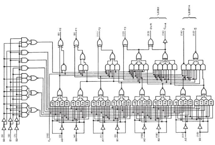
10 C0 C1 C2 A B F FORMALIZE THE PROBLEM choose implementation technology 5-variable K-map to discrete gates multiplexer implementation the target operations are pair wise inverse of each other A B A B A B :1 MUX S2 S1 S0 C0 C1 C2 F MSI EXAMPLE: 74381/382 ALU Eight-operation functional block ( limited ALU) handling two 4-bit words. Three logic operations, three arithmetic operations, clear and preset operations. 10
11 11
12 ARITHMETIC CIRCUITS Excellent Examples of Combinational Logic Design Time vs. Space Trade-offs Doing things fast may require more logic and thus more space Example: carry lookahead logic Arithmetic and Logic Units General-purpose building blocks Critical components of processor datapaths Used within most computer instructions ARITHMETIC CIRCUITS: BASIC BUILDING BLOCKS Below I will discuss those combinational logic building blocks that can be used to perform addition and subtraction operations on binary numbers. Addition and subtraction are the two most commonly used arithmetic operations, as the other two, namely multiplication and division, are respectively the processes of repeated addition and repeated subtraction. We will begin with the basic building blocks that form the basis of all hardware used to perform the aforesaid arithmetic operations on binary numbers. These include half-adder, full adder, half-subtractor, full subtractor and controlled inverter. 12
13 CCIRCUITS FOR BINARY ADDITION Half adder (add two 1-bit numbers) Sum = Ai' Bi + Ai Bi' = Ai xor Bi Cout = Ai Bi Full adder (carry-in to cascade for multi-bit adders) Sum = Ci xor A xor B Cout = B Ci + A Ci + A B = Ci (A + B) + A B Ai Bi Sum Cout Ai Bi Cin Sum Cout FULL ADDER IMPLEMENTATIONS Standard approach 6 gates 2 XORs, 2 ANDs, 2 ORs Alternative implementation 5 gates half adder is an XOR gate and AND gate 2 XORs, 2 ANDs, 1 OR A B Cin A B A B Cin Cout = A B + Cin (A xor B) = A B + B Cin + A Cin S Cout A B Cin Half Adder Cout A xor B A B Sum Half Adder Cout A xor B xor Cin Cin (A xor B) Sum Sum Cout 13
14 HALF- AND FULL SUBTRACTOR The subtraction of two given binary numbers can be carried out by adding 2 s complement of the subtrahend to the minuend. This allows us to do a subtraction operation with adder circuits. However, we will also briefly look at the counterparts of half-adder and full adder circuits in the half-subtractor and full subtractor for direct implementation of subtraction operations using logic gates. HALF-SUBTRACTOR A half-subtractor is a combinational circuit that can be used to subtract one binary digit from another to produce a DIFFERENCE output and a BORROW output. The BORROW output here specifies whether a 1 has been borrowed to perform the subtraction. 14
15 FULL SUBTRACTOR A full subtractor performs subtraction operation on two bits, a minuend and a subtrahend, and also takes into consideration whether a 1 has already been borrowed by the previous adjacent lower minuend bit or not. As a result, there are three bits to be handled at the input of a full subtractor, namely the two bits to be subtracted and a borrow bit designated as Bin. There are two outputs, namely the DIFFERENCE output D and the BORROW output Bo. The BORROW output bit tells whether the minuend bit needs to borrow a 1 from the next possible higher minuend bit. FULL SUBTRACTOR Truth table of a full subtractor 15
16 FULL SUBTRACTOR Logic implementation of a full subtractor with half-subtractors. CONTROLLED INVERTER A controlled inverter is needed when an adder is to be used as a subtractor. Subtraction is addition of the 2 s complement of the subtrahend to the minuend. Thus, the first step towards implementation of a subtractor is to determine the 2 s complement of the subtrahend. And for this, one needs firstly to find 1 s complement. A controlled inverter is used to find 1 s complement. A one-bit controlled inverter is a two-input EX-OR gate with one of its inputs treated as a control input. Eight-bit controlled inverter 16
17 ADDER/SUBTRACTOR Use an adder to do subtraction thanks to 2s complement representation A B = A + ( B) = A + B' + 1 Control signal selects B or 2s complement of B A3 B3 B3' A2 B2 B2' A1 B1 B1' A0 B0 B0' 0 1 Sel 0 1 Sel 0 1 Sel 0 1 Sel A B Cout Cin Sum A B Cout Cin Sum A B Cout Cin Sum A B Cout Cin Sum Add' Subtract S3 S2 S1 S0 Overflow TWO S COMPLEMENT ADDER/SUBTRACTOR Q = (q 3 q 2 q 1 q 0 ) 2 P = (p 3 p 2 p 1 p 0 ) 2 4A3A2A 1A 4B 3B 2B MUX (74157) 4Y 3Y 2Y 1Y 1B S G Select A4 A3 A2 A1 B4 B3 B2 B1 C4 ADDER (7483) S4 S3 S2 S1 C0 Select 0 1 Function R = P + Q R = P + Q + 1 R = (r 4 r 3 r 2 r 1 ) 2 17
18 RIPPLE CARRY ADDER The full adder is for adding two operands that are only one bit wide. To add two operands that are, say four bits wide, we connect four full adders together in series. The resulting circuit is called a ripple carry adder for adding two 4-bit operands. The ripple-carry adder is slow because the carry-in for each full adder is dependent on the carry-out signal from the previous FA. So before FA i can output valid data, it must wait for FA i 1 to have valid data. CARRY-LOOKAHEAD ADDER The layout of a ripple carry adder is simple, which allows for fast design time, however, the ripple carry adder is relatively slow, since each full adder must wait for the carry bit from the previous full adder. From C in to C out 2 gates should be passed through. Ergo a 32-bit adder requires 31 carry computations and the final sum calculation for a total of 31x2 + 1 = 63 gate delays. In the carry-lookahead adder, each bit slice eliminates this dependency on the previous carry-out signal and instead uses the values of the two input operands, directly to deduce the needed signals. This is possible from the following observations regarding the carry-out signal. 18
19 FULL ADDER: GENERATION AND PROPAGATION OF CARRY A B Cin Full adder Sum Cout C o = A B + (A B)C i or C o = A B + (A + B)C i C o = G + P C i Define G and P auxiliary functions RIPPLE-CARRY ADDERS Critical Delay The propagation of carry from low to high order stages Cin A B late @1 two gate delays to compute Cout A0 B0 A1 B1 A2 B2 4 stage adder A B Cin S A3 B3 19
 for each bit position, and using them the carries for each position are created.")
20 CRITICAL PATH TROUGH A RIPPLE CARRY ADDER CARRY LOOK-AHEAD ADDER Carry look-ahead adders reduce the computation time. They work creating propagate and generate signals (P and G) for each bit position, and using them the carries for each position are created. Some multi-bit adder architectures break the adder into blocks. It is possible to vary the length of these blocks based on the propagation delay of the circuits to optimize computation time. These block based adders include the carry bypass adder which will determine P and G for each block rather than each bit, and the carry select adder which pre-generates sum and carry values for either possible carry input to the block. 20
21 Operands FASTER ADDITION: CARRY LOOKAHEAD LOGIC Carry Logic Sum Principal layout of carry lookahead adder. CARRY-LOOKAHEAD LOGIC Carry generate: Gi = Ai Bi Must generate carry when A = B = 1 Carry propagate: Pi = Ai xor Bi Carry-in will equal carry-out here Sum and Cout can be re-expressed in terms of generate/propagate: Si = Ai xor Bi xor Ci = Pi xor Ci Ci+1= Ai Bi + Ai Ci + Bi Ci = Ai Bi + Ci (Ai + Bi) = Ai Bi + Ci (Ai xor Bi) = Gi + Ci Pi 21
22 CARRY-LOOKAHEAD LOGIC Re-express the carry logic as follows: C1 = G0 + P0 C0 C2 = G1 + P1 C1 = G1 + P1 G0 + P1 P0 C0 C3 = G2 + P2 C2 = G2 + P2 G1 + P2 P1 G0 + P2 P1 P0 C0 C4 = G3 + P3 C3 = G3 + P3 G2 + P3 P2 G1 + P3 P2 P1 G0 + P3 P2 P1 P0 C0 Each of the carry equations can be implemented with two-level logic All inputs are now directly derived from data inputs and not from intermediate carries this allows computation of all sum outputs to proceed in parallel CARRY-LOOKAHEAD IMPLEMENTATION Adder with propagate and generate outputs Ai Bi Ci 1 gate delay 2 gate delays 1 gate delay increasingly complex logic for carries C0 P0 G0 C0 P0 P1 G0 P1 G1 C1 C2 C0 P0 P1 P2 G0 P1 P2 G1 P2 G2 C0 P0 P1 P2 P3 G0 P1 P2 C3 P3 G1 P2 P3 G2 P3 G3 C4 22
23 CARRY LOOKAHEAD CIRCUITRY (a) Circuit for generating the carry-lookahead signals, c1 to c4; (b) One bit slice of the carry-lookahead adder. CARRY-LOOKAHEAD IMPLEMENTATION Carry-lookahead logic generates individual carries Sums computed much more quickly in parallel However, cost of carry logic increases with more stages Cin Cin A0 B0 A0 B0 A1 B1 A2 B2 A3 B3 A1 B1 A2 B2 A3 B3 23
24 4-BIT CARRY LOOKAHEAD ADDER CIRCUIT carry-out, not c-zero Total 26 gates, c.f. 4 standard full adders 4x6 = 24 gates 74HC/HCT181 4-BIT ALU LOGIC DIAGRAM 24
25 CARRY LOOKAHEAD ADDERS: FEATURES By adding more hardware, we reduced the number of levels in the circuit and sped things up. We can cascade carry lookahead adders, just like ripple carry adders. (We d have to do carry lookahead between the adders too.) How much faster is this? For a 4-bit adder, not much. There are 4 gates in the longest path of a carry lookahead adder, versus 9 gates for a ripple carry adder. But if we do the cascading properly, a 16-bit carry lookahead adder could have only 8 gates in the longest path, as opposed to 33 for a ripple carry adder. Newer CPUs these days use 64-bit adders. That s 12 vs. 129 gates! The delay of a carry lookahead adder grows logarithmically with the size of the adder, while a ripple carry adder s delay grows linearly. The thing to remember about this is the trade-off between complexity and performance. Ripple carry adders are simpler, but slower. Carry lookahead adders are faster but more complex. CARRYLOOKAHEAD ADDERS WITH CASCDED CARRY-LOOKAHEAD LOGIC Carry-lookahead adder 4 four-bit adders with internal carry lookahead Second level carry lookahead unit extends lookahead to 16 bits A[15-12] B[15-12] 4-bit Adder C12 P G 4 A[11-8] B[11-8] 4-bit Adder C8 P G 4 A[7-4] B[7-4] 4-bit Adder C4 P G 4 A[3-0] B[3-0] 4-bit Adder P G C16 P3 G3 C3 P2 G2 C2 P1 G1 C1 Lookahead Carry Unit P0 G0 C0 25

26 CARRY-SELECT ADDER Redundant hardware to make carry calculation go faster Compute two high-order sums in parallel while waiting for carry-in One assuming carry-in is 0 and another assuming carry-in is 1 Select correct result once carry-in is finally computed C8 4-bit adder [7:4] 1 adder high C8 4-bit adder [7:4] 0 adder low five 2:1 mux C4 4-Bit Adder [3:0] C0 C8 S7 S6 S5 S4 S3 S2 S1 S0 CARRY-SELECT ADDERS 26
27 MULTILEVEL CARRY-SELECT ADDERS ARITHMETICAL OPERATIONS IN BCD Many digital systems (processors, computers) can perform the arithmetical operations or a part of them directly on BCD numbers. E.g. the microprocessors can perform BCD addition, several of them subtraction too. Certain special processors can perform BCD multiplication and division too. The BCD addition is reduced to binary addition. The tetrades of the operands are added as binary numbers, and if necessary (illegal codewords or decimal carry is generated during the addition), a systematic correction is performed
28 ADDITION IN NORMAL BCD (8421) CODE If the sum of two tetrades is not larger than 9, the result is valid, no correction is necessary. If the sum of two tetrades is larger than 9, (decimal carry and illegal codeword or pseudotetrade is generated) the result is valid only in binary system and not in BCD. The necessary correction is to add decimal 6 or i.e. binary 0110 to the actual tetrade. The correction should be performed beginning form the least significant tetrade and going upwards step-by-step. 55 FUNCTIONAL DIAGRAM OF A BCD ADDER (1 DIGIT) C4 B3 B2 B1 B0 B3 B2 B1 B0 C4 Binary adder & 1 & 0 0 B3 B2 B1 B0 Binary adder A3 A2 A1 A0 A3 A2 A1 A0 C0 S3 S2 S1 S0 A3 A2 A1 A0 C0 S3 S2 S1 S0 S3 S2 S1 S0 0 0 The first adder adds the two codes corresponding to the k-th decimal place, the second adds 6 if necessary
29 SUBTRACTION IN BCD (8421) CODE In BCD as in binary, the subtraction is performed by complementing (the subtrahend) and addition. Generally 9 s complement is used. The circuit generating the 9 s complement can be constructed from common gates or form more complex functional elements. 57 GENERATING 9 S COMPLEMENT IN BCD A 3 A 2 A 1 A 0 =1 =1 =1 =1 V 0 0 If V = 0 then X k = A k 4-BIT ADDER If V = 1 then 8X 3 +4X 2 +2X 1 +X 0 = = 9 (8A 3 +4A 2 +2A 1 +A 0 ) X 3 X 2 X 1 X 0 29
30 SSI MODULAR LOGIC: 4-BIT BCD ADDER 59 SSI MODULAR LOGIC: 4-BIT BCD ADDER The 74F583 4-bit coded (BCD) full adder performs the addition of two decimal numbers (A0 A3, B0 B3). The look-ahead generates BCD carry terms internally, allowing the 74F583 to do BCD addition correctly. For BCD numbers 0 through 9 at A and B inputs, the BCD sum forms at the output. In addition of two BCD numbers totalling a number greater than 9, a valid BCD number and carry will result
31 4-BIT BCD ADDER LOGIC DIAGRAM 74F583 Gate count 75 (incl. inverters) 61 MULTIPLIERS A binary multiplier is an electronic circuit used in digital electronics, such as a computer, to multiply two binary numbers. A variety of computer arithmetic techniques can be used to implement a digital multiplier. Most techniques involve computing a set of partial products, and then summing the partial products together. This process is similar to the method taught to primary school children for conducting long multiplication on base-10 integers, but has been modified here for application to a base-2 (binary) numeral system. The first stage of most multipliers involves generating the partial products which is nothing but an array of AND gates. An n-bit by n-nit multiplier requires n 2 AND gates for partial product generation. The partial products are then added to give the final results. 31
32 THEORY OF MULTIPLICATION Basic Concept multiplicand multiplier * 1101 (13) 1011 (11) 1101 Partial products (143) product of two 4-bit numbers is an 8-bit number COMBINATIONAL MULTIPLIER Partial Product Accumulation A3 A2 A1 A0 B3 B2 B1 B0 A2 B0 A2B0 A1 B0 A0 B0 A3 B1 A2 B1 A1 B1 A0 B1 A3 B2 A2 B2 A1 B2 A0 B2 A3 B3 A2 B3 A1 B3 A0 B3 S7 S6 S5 S4 S3 S2 S1 S0 32
33 THE ARRAY MULTIPLIER (4x4 BIT) PARTIAL PRODUCT ACCUMULATION A 3 B 3 A 3 B 2 A 2 B 3 A 3 B 1 A 2 B 2 A 1 B 3 A 3 B 0 A 2 B 1 A 1 B 2 A 0 B 3 A 2 B 0 A 1 B 1 A 0 B 2 A 0 B 1 A 1 B 0 A 0 B 0 F A HA HA HA F A F A F A F A F A F A HA F A S 7 S 6 S 5 S 4 S 3 S 2 S 1 S 0 Note use of parallel carry-outs to form higher order sums 12 Adders, if full adders, this is 6 gates each = 72 gates 16 gates form the partial products total = 88 gates! 33

34 SSI REALIZATION OF 4x4 BIT MULTIPLIER 67 COMBIATIONAL MULTIPLIER Sum In X Cin Another Representation of the Circuit Building block: FULL ADDER + AND Y F A A CO S B CI Cout Sum Out A3 A2 A1 A0 B0 C A3 B0 S C A2 B0 S C A1 B0 S C A0 B0 S B1 A3 B1 A2 B1 A1 B1 A0 B1 C C C C S S S S B2 C A3 B2 S C A2 B2 S C A1 B2 S C A0 B2 S B3 A3 B3 A2 B3 A1 B3 A0 B3 C S S S S P7 P6 P5 P4 P3 P2 P1 P0 4 x 4 array of building blocks 34

 N2 = (2 4 H2 + L2) Multiplying out N1N2 = 2 8 H1H2 + 2 4 (H1L2 + H2L1) + L1L2")
35 MAKING A 2n-BIT MULTIPLIER USING n-bit MULTIPLIERS E.g. in the case of a 8-bit multiplier, it is possible to partition the problem by splitting both the multiplier and multiplicand into two 4-bit words. N1 = (2 4 H1 + L1) N2 = (2 4 H2 + L2) Multiplying out N1N2 = 2 8 H1H (H1L2 + H2L1) + L1L2 MAKING A 2n-BIT MULTIPLIER USING n-bit MULTIPLIERS Given n-bit multipliers: Synthesize 2n-bit multipliers: 35


36 MAKING A 2n-BIT MULTIPLIER USING n-bit MULTIPLIERS 2n-bit by 2n-bit multiplication: 1. Divide multiplicands into n-bit pieces 2. Form 2n-bit partial products, using n-bit by n-bit multipliers. 3. Align appropriately 4. Add. REGROUP partial products 2 additions rather than 3! Induction: we can use the same structuring principle to build a 4n-bit multiplier from our newly-constructed 2n-bit ones... MULTIPLIER: MODULAR STRUCTURE 8 x 8 bit multiplier built from 4 x 4 bit modules 72 36
37 MULTIPLIER: MODULAR STRUCTURE 8 x 8 bit multiplier built from 4 x 4 bit modules Product MSB : 0, LSB: 15) 73 ROM IMPLEMENTED MULTIPLIER Binary multiplication can be achieved by using a ROM as a look-up table. E.g., multiplication of two 4-bit numbers requires a ROM having eight address lines, four of them X4XRX2X1 being allocated to the multiplier, and the remaining four, Y4Y3Y2Y1 to the multiplicand. Since the multiplication of two 4-bit numbers can result in a doublelength product, the ROM should have eight output lines, and a room with capacity of 256 bytes is required. For two 8-bit numbers 2 16 = memory locations and 16 output lines for the double-length products are required. This requires a ROM of 128 kbytes. For 16-bit multiplication the required ROM capacity is formidable (16 Gbytes!). 37
38 8x8 BIT COMBINATIONAL MULTIPLIER 4x4 bit partial products are generated by four 256x8 bit ROMs MULTIPLICATION: NEGATIVE NUMBERS The basic school method of multiplication handles the sign with a separate rule ("+ with + yields +", "+ with - yields -", etc.). Modern computers embed the sign of the number in the number itself, usually in the two s complement representation. That forces the multiplication process to be adapted to handle two's complement numbers, and that complicates the process a bit more. Similarly, processors that use one s complement sign-and-magnitude, IEEE-754 or other binary representations require specific adjustments to the multiplication process. 38
39 MULTIPLICATION: SPEEDIN UP Older multiplier architectures employed a shifter and accumulator to sum each partial product, often one partial product per cycle, trading off speed for die area. Modern multiplier architectures use the Baugh-Wooley algorithm, Wallace tree or Dadda to add the partial products together in a single cycle. The performance of the Wallace tree implementation is sometimes improved by modified Booth encoding one of the two multiplicands, which reduces the number of partial products that must be summed. BOOTH ENCODING MULTIPLIER System layout of Booth encoding 8-bit multiplier 39
40 BOOTH ENCODING MULTIPLIER The multiplier takes in 2 8-bits operands: the multiplier(mr) and the multiplicand (MD), then produces 16-bit multiplication result of the two as its output. The architecture comprises four parts: Complement Generator, Booth Encoder, Partial Product and Carry Lookahead Adder. BOOTH ENCODING DEMO 40
Chapter 4. Combinational: Circuits with logic gates whose outputs depend on the present combination of the inputs. elements. Dr.
 Chapter 4 Dr. Panos Nasiopoulos Combinational: Circuits with logic gates whose outputs depend on the present combination of the inputs. Sequential: In addition, they include storage elements Combinational
CSE140: Components and Design Techniques for Digital Systems. Decoders, adders, comparators, multipliers and other ALU elements. Tajana Simunic Rosing
 CSE4: Components and Design Techniques for Digital Systems Decoders, adders, comparators, multipliers and other ALU elements Tajana Simunic Rosing Mux, Demux Encoder, Decoder 2 Transmission Gate: Mux/Tristate
Binary addition by hand. Adding two bits
 Chapter 3 Arithmetic is the most basic thing you can do with a computer We focus on addition, subtraction, multiplication and arithmetic-logic units, or ALUs, which are the heart of CPUs. ALU design Bit
Overview. Arithmetic circuits. Binary half adder. Binary full adder. Last lecture PLDs ROMs Tristates Design examples
 Overview rithmetic circuits Last lecture PLDs ROMs Tristates Design examples Today dders Ripple-carry Carry-lookahead Carry-select The conclusion of combinational logic!!! General-purpose building blocks
Hardware Design I Chap. 4 Representative combinational logic
 Hardware Design I Chap. 4 Representative combinational logic E-mail: shimada@is.naist.jp Already optimized circuits There are many optimized circuits which are well used You can reduce your design workload
Combinational Logic Design Arithmetic Functions and Circuits
 Combinational Logic Design Arithmetic Functions and Circuits Overview Binary Addition Half Adder Full Adder Ripple Carry Adder Carry Look-ahead Adder Binary Subtraction Binary Subtractor Binary Adder-Subtractor
EECS150. Arithmetic Circuits
 EE5 ection 8 Arithmetic ircuits Fall 2 Arithmetic ircuits Excellent Examples of ombinational Logic Design Time vs. pace Trade-offs Doing things fast may require more logic and thus more space Example:
Logic. Combinational. inputs. outputs. the result. system can
 Digital Electronics Combinational Logic Functions Digital logic circuits can be classified as either combinational or sequential circuits. A combinational circuit is one where the output at any time depends
Systems I: Computer Organization and Architecture
 Systems I: Computer Organization and Architecture Lecture 6 - Combinational Logic Introduction A combinational circuit consists of input variables, logic gates, and output variables. The logic gates accept
Class Website:
 ECE 20B, Winter 2003 Introduction to Electrical Engineering, II LECTURE NOTES #5 Instructor: Andrew B. Kahng (lecture) Email: abk@ece.ucsd.edu Telephone: 858-822-4884 office, 858-353-0550 cell Office:
COMBINATIONAL LOGIC FUNCTIONS
 COMBINATIONAL LOGIC FUNCTIONS Digital logic circuits can be classified as either combinational or sequential circuits. A combinational circuit is one where the output at any time depends only on the present
Adders, subtractors comparators, multipliers and other ALU elements
 CSE4: Components and Design Techniques for Digital Systems Adders, subtractors comparators, multipliers and other ALU elements Instructor: Mohsen Imani UC San Diego Slides from: Prof.Tajana Simunic Rosing
Adders, subtractors comparators, multipliers and other ALU elements
 CSE4: Components and Design Techniques for Digital Systems Adders, subtractors comparators, multipliers and other ALU elements Adders 2 Circuit Delay Transistors have instrinsic resistance and capacitance
CMPUT 329. Circuits for binary addition
 CMPUT 329 Parallel Adder with Carry Lookahead and ALU Ioanis Nikolaidis (Katz & Borriello) rcuits for binary addition Full adder (carry-in to cascade for multi-bit adders) Sum = xor A xor B Cout = B +
Chapter 5 Arithmetic Circuits
 Chapter 5 Arithmetic Circuits SKEE2263 Digital Systems Mun im/ismahani/izam {munim@utm.my,e-izam@utm.my,ismahani@fke.utm.my} February 11, 2016 Table of Contents 1 Iterative Designs 2 Adders 3 High-Speed
Section 3: Combinational Logic Design. Department of Electrical Engineering, University of Waterloo. Combinational Logic
 Section 3: Combinational Logic Design Major Topics Design Procedure Multilevel circuits Design with XOR gates Adders and Subtractors Binary parallel adder Decoders Encoders Multiplexers Programmed Logic
Logic and Computer Design Fundamentals. Chapter 5 Arithmetic Functions and Circuits
 Logic and Computer Design Fundamentals Chapter 5 Arithmetic Functions and Circuits Arithmetic functions Operate on binary vectors Use the same subfunction in each bit position Can design functional block
UNIT II COMBINATIONAL CIRCUITS:
 UNIT II COMBINATIONAL CIRCUITS: INTRODUCTION: The digital system consists of two types of circuits, namely (i) (ii) Combinational circuits Sequential circuits Combinational circuit consists of logic gates
Combinational Logic. By : Ali Mustafa
 Combinational Logic By : Ali Mustafa Contents Adder Subtractor Multiplier Comparator Decoder Encoder Multiplexer How to Analyze any combinational circuit like this? Analysis Procedure To obtain the output
IT T35 Digital system desigm y - ii /s - iii
 UNIT - II Combinational Logic Adders subtractors code converters binary parallel adder decimal adder magnitude comparator encoders decoders multiplexers demultiplexers-binarymultiplier Parity generator
Carry Look Ahead Adders
 Carry Look Ahead Adders Lesson Objectives: The objectives of this lesson are to learn about: 1. Carry Look Ahead Adder circuit. 2. Binary Parallel Adder/Subtractor circuit. 3. BCD adder circuit. 4. Binary
ARITHMETIC COMBINATIONAL MODULES AND NETWORKS
 ARITHMETIC COMBINATIONAL MODULES AND NETWORKS 1 SPECIFICATION OF ADDER MODULES FOR POSITIVE INTEGERS HALF-ADDER AND FULL-ADDER MODULES CARRY-RIPPLE AND CARRY-LOOKAHEAD ADDER MODULES NETWORKS OF ADDER MODULES
Combinational Logic. Mantıksal Tasarım BBM231. section instructor: Ufuk Çelikcan
 Combinational Logic Mantıksal Tasarım BBM23 section instructor: Ufuk Çelikcan Classification. Combinational no memory outputs depends on only the present inputs expressed by Boolean functions 2. Sequential
14:332:231 DIGITAL LOGIC DESIGN
 4:332:23 DIGITAL LOGIC DEIGN Ivan Marsic, Rutgers University Electrical & Computer Engineering Fall 23 Lecture #4: Adders, ubtracters, and ALUs Vector Binary Adder [Wakerly 4 th Ed., ec. 6., p. 474] ingle
CMSC 313 Lecture 18 Midterm Exam returned Assign Homework 3 Circuits for Addition Digital Logic Components Programmable Logic Arrays
 CMSC 33 Lecture 8 Midterm Exam returned ssign Homework 3 Circuits for ddition Digital Logic Components Programmable Logic rrays UMC, CMSC33, Richard Chang Half dder Inputs: and Outputs:
Combina-onal Logic Chapter 4. Topics. Combina-on Circuit 10/13/10. EECE 256 Dr. Sidney Fels Steven Oldridge
 Combina-onal Logic Chapter 4 EECE 256 Dr. Sidney Fels Steven Oldridge Topics Combina-onal circuits Combina-onal analysis Design procedure simple combined to make complex adders, subtractors, converters
Combinational Logic. Lan-Da Van ( 范倫達 ), Ph. D. Department of Computer Science National Chiao Tung University Taiwan, R.O.C.
, Ph. D. Department of Computer Science National Chiao Tung University Taiwan, R.O.C.") Combinational Logic ( 范倫達 ), Ph. D. Department of Computer Science National Chiao Tung University Taiwan, R.O.C. Fall, 2017 ldvan@cs.nctu.edu.tw http://www.cs.nctu.edu.tw/~ldvan/ Combinational Circuits
Combinational Logic ( 范倫達 ), Ph. D. Department of Computer Science National Chiao Tung University Taiwan, R.O.C. Fall, 2017 ldvan@cs.nctu.edu.tw http://www.cs.nctu.edu.tw/~ldvan/ Combinational Circuits
CSE140: Components and Design Techniques for Digital Systems. Logic minimization algorithm summary. Instructor: Mohsen Imani UC San Diego
 CSE4: Components and Design Techniques for Digital Systems Logic minimization algorithm summary Instructor: Mohsen Imani UC San Diego Slides from: Prof.Tajana Simunic Rosing & Dr.Pietro Mercati Definition
CS 140 Lecture 14 Standard Combinational Modules
 CS 14 Lecture 14 Standard Combinational Modules Professor CK Cheng CSE Dept. UC San Diego Some slides from Harris and Harris 1 Part III. Standard Modules A. Interconnect B. Operators. Adders Multiplier
Menu. Binary Adder EEL3701 EEL3701. Add, Subtract, Compare, ALU
 Other MSI Circuit: Adders >Binar, Half & Full Canonical forms Binar Subtraction Full-Subtractor Magnitude Comparators >See Lam: Fig 4.8 ALU Menu Look into m... 1 Binar Adder Suppose we want to add two
Review for Test 1 : Ch1 5
 Review for Test 1 : Ch1 5 October 5, 2006 Typeset by FoilTEX Positional Numbers 527.46 10 = (5 10 2 )+(2 10 1 )+(7 10 0 )+(4 10 1 )+(6 10 2 ) 527.46 8 = (5 8 2 ) + (2 8 1 ) + (7 8 0 ) + (4 8 1 ) + (6 8
Digital System Design Combinational Logic. Assoc. Prof. Pradondet Nilagupta
 Digital System Design Combinational Logic Assoc. Prof. Pradondet Nilagupta pom@ku.ac.th Acknowledgement This lecture note is modified from Engin112: Digital Design by Prof. Maciej Ciesielski, Prof. Tilman
UNSIGNED BINARY NUMBERS DIGITAL ELECTRONICS SYSTEM DESIGN WHAT ABOUT NEGATIVE NUMBERS? BINARY ADDITION 11/9/2018
 DIGITAL ELECTRONICS SYSTEM DESIGN LL 2018 PROFS. IRIS BAHAR & ROD BERESFORD NOVEMBER 9, 2018 LECTURE 19: BINARY ADDITION, UNSIGNED BINARY NUMBERS For the binary number b n-1 b n-2 b 1 b 0. b -1 b -2 b
PG - TRB UNIT-X- DIGITAL ELECTRONICS. POLYTECHNIC-TRB MATERIALS
 SRIMAAN COACHING CENTRE-PG-TRB-PHYSICS- DIGITAL ELECTRONICS-STUDY MATERIAL-CONTACT: 8072230063 SRIMAAN PG - TRB PHYSICS UNIT-X- DIGITAL ELECTRONICS POLYTECHNIC-TRB MATERIALS MATHS/COMPUTER SCIENCE/IT/ECE/EEE
Design of Sequential Circuits
 Design of Sequential Circuits Seven Steps: Construct a state diagram (showing contents of flip flop and inputs with next state) Assign letter variables to each flip flop and each input and output variable
Combinational Logic. Lan-Da Van ( 范倫達 ), Ph. D. Department of Computer Science National Chiao Tung University Taiwan, R.O.C.
, Ph. D. Department of Computer Science National Chiao Tung University Taiwan, R.O.C.") Combinational Logic ( 范倫達 ), Ph. D. Department of Computer Science National Chiao Tung University Taiwan, R.O.C. Fall, 2010 ldvan@cs.nctu.edu.tw http://www.cs.nctu.edu.tw/~ldvan/ Combinational Circuits
Combinational Logic ( 范倫達 ), Ph. D. Department of Computer Science National Chiao Tung University Taiwan, R.O.C. Fall, 2010 ldvan@cs.nctu.edu.tw http://www.cs.nctu.edu.tw/~ldvan/ Combinational Circuits
ว ตถ ประสงค ของบทเร ยน
 Logic Design with MSI Circuits ว ตถ ประสงค ของบทเร ยน ร จ กวงจรประเภท MSI เข าใจการทำงานของวงจร MSI ท ม ใช อย ท วไป สามารถประย กต ใช วงจร MSI ในการออกแบบวงจรลอจ กแบบต างๆ ได A. Yaicharoen 1 Type of Circuits
ECE 545 Digital System Design with VHDL Lecture 1. Digital Logic Refresher Part A Combinational Logic Building Blocks
 ECE 545 Digital System Design with VHDL Lecture Digital Logic Refresher Part A Combinational Logic Building Blocks Lecture Roadmap Combinational Logic Basic Logic Review Basic Gates De Morgan s Law Combinational
Binary addition (1-bit) P Q Y = P + Q Comments Carry = Carry = Carry = Carry = 1 P Q
 P Q Y = P + Q Comments Carry = Carry = Carry = Carry = 1 P Q") Digital Arithmetic In Chapter 2, we have discussed number systems such as binary, hexadecimal, decimal, and octal. We have also discussed sign representation techniques, for example, sign-bit representation
Digital Arithmetic In Chapter 2, we have discussed number systems such as binary, hexadecimal, decimal, and octal. We have also discussed sign representation techniques, for example, sign-bit representation
211: Computer Architecture Summer 2016
 211: Computer Architecture Summer 2016 Liu Liu Topic: Storage Project3 Digital Logic - Storage: Recap - Review: cache hit rate - Project3 - Digital Logic: - truth table => SOP - simplification: Boolean
ELEN Electronique numérique
 ELEN0040 - Electronique numérique Patricia ROUSSEAUX Année académique 2014-2015 CHAPITRE 3 Combinational Logic Circuits ELEN0040 3-4 1 Combinational Functional Blocks 1.1 Rudimentary Functions 1.2 Functions
CMPEN 411 VLSI Digital Circuits Spring Lecture 19: Adder Design
 CMPEN 411 VLSI Digital Circuits Spring 2011 Lecture 19: Adder Design [Adapted from Rabaey s Digital Integrated Circuits, Second Edition, 2003 J. Rabaey, A. Chandrakasan, B. Nikolic] Sp11 CMPEN 411 L19
Review: Additional Boolean operations
 Review: Additional Boolean operations Operation: NAND (NOT-AND) NOR (NOT-OR) XOR (exclusive OR) Expressions: (xy) = x + y (x + y) = x y x y = x y + xy Truth table: x y (xy) x y (x+y) x y x y 0 0 1 0 1
CSEE 3827: Fundamentals of Computer Systems. Combinational Circuits
 CSEE 3827: Fundamentals of Computer Systems Combinational Circuits Outline (M&K 3., 3.3, 3.6-3.9, 4.-4.2, 4.5, 9.4) Combinational Circuit Design Standard combinational circuits enabler decoder encoder
Sample Test Paper - I
 Scheme G Sample Test Paper - I Course Name : Computer Engineering Group Marks : 25 Hours: 1 Hrs. Q.1) Attempt any THREE: 09 Marks a) Define i) Propagation delay ii) Fan-in iii) Fan-out b) Convert the following:
CHAPTER1: Digital Logic Circuits Combination Circuits
 CS224: Computer Organization S.KHABET CHAPTER1: Digital Logic Circuits Combination Circuits 1 PRIMITIVE LOGIC GATES Each of our basic operations can be implemented in hardware using a primitive logic gate.
Digital Integrated Circuits A Design Perspective. Arithmetic Circuits. Jan M. Rabaey Anantha Chandrakasan Borivoje Nikolic.
 Digital Integrated Circuits A Design Perspective Jan M. Rabaey Anantha Chandrakasan Borivoje Nikolic Arithmetic Circuits January, 2003 1 A Generic Digital Processor MEMORY INPUT-OUTPUT CONTROL DATAPATH
Midterm Exam Two is scheduled on April 8 in class. On March 27 I will help you prepare Midterm Exam Two.
 Announcements Midterm Exam Two is scheduled on April 8 in class. On March 27 I will help you prepare Midterm Exam Two. Chapter 5 1 Chapter 3: Part 3 Arithmetic Functions Iterative combinational circuits
We are here. Assembly Language. Processors Arithmetic Logic Units. Finite State Machines. Circuits Gates. Transistors
 CSC258 Week 3 1 Logistics If you cannot login to MarkUs, email me your UTORID and name. Check lab marks on MarkUs, if it s recorded wrong, contact Larry within a week after the lab. Quiz 1 average: 86%
Chapter 2 (Lect 2) Canonical and Standard Forms. Standard Form. Other Logic Operators Logic Gates. Sum of Minterms Product of Maxterms
 Canonical and Standard Forms. Standard Form. Other Logic Operators Logic Gates. Sum of Minterms Product of Maxterms") Chapter 2 (Lect 2) Canonical and Standard Forms Sum of Minterms Product of Maxterms Standard Form Sum of products Product of sums Other Logic Operators Logic Gates Basic and Multiple Inputs Positive and
Chapter 2 (Lect 2) Canonical and Standard Forms Sum of Minterms Product of Maxterms Standard Form Sum of products Product of sums Other Logic Operators Logic Gates Basic and Multiple Inputs Positive and
ELCT201: DIGITAL LOGIC DESIGN
 ELCT2: DIGITAL LOGIC DESIGN Dr. Eng. Haitham Omran, haitham.omran@guc.edu.eg Dr. Eng. Wassim Alexan, wassim.joseph@guc.edu.eg Lecture 4 Following the slides of Dr. Ahmed H. Madian محرم 439 ه Winter 28
Chapter 5. Digital Design and Computer Architecture, 2 nd Edition. David Money Harris and Sarah L. Harris. Chapter 5 <1>
 Chapter 5 Digital Design and Computer Architecture, 2 nd Edition David Money Harris and Sarah L. Harris Chapter 5 Chapter 5 :: Topics Introduction Arithmetic Circuits umber Systems Sequential Building
Computer Science 324 Computer Architecture Mount Holyoke College Fall Topic Notes: Digital Logic
 Computer Science 324 Computer Architecture Mount Holyoke College Fall 2007 Topic Notes: Digital Logic Our goal for the next few weeks is to paint a a reasonably complete picture of how we can go from transistor
CMSC 313 Lecture 18 Midterm Exam returned Assign Homework 3 Circuits for Addition Digital Logic Components Programmable Logic Arrays
 MS 33 Lecture 8 Midterm Exam returned Assign Homework 3 ircuits for Addition Digital Logic omponents Programmable Logic Arrays UMB, MS33, Richard hang MS 33, omputer Organization & Assembly
Introduction to Digital Logic Missouri S&T University CPE 2210 Subtractors
 Introduction to Digital Logic Missouri S&T University CPE 2210 Egemen K. Çetinkaya Egemen K. Çetinkaya Department of Electrical & Computer Engineering Missouri University of Science and Technology cetinkayae@mst.edu
Design of Combinational Logic
 Pune Vidyarthi Griha s COLLEGE OF ENGINEERING, NASHIK 3. Design of Combinational Logic By Prof. Anand N. Gharu (Assistant Professor) PVGCOE Computer Dept.. 30 th June 2017 CONTENTS :- 1. Code Converter
3. Combinational Circuit Design
 CSEE 3827: Fundamentals of Computer Systems, Spring 2 3. Combinational Circuit Design Prof. Martha Kim (martha@cs.columbia.edu) Web: http://www.cs.columbia.edu/~martha/courses/3827/sp/ Outline (H&H 2.8,
Digital Electronics Circuits 2017
 JSS SCIENCE AND TECHNOLOGY UNIVERSITY Digital Electronics Circuits (EC37L) Lab in-charge: Dr. Shankraiah Course outcomes: After the completion of laboratory the student will be able to, 1. Simplify, design
EECS150 - Digital Design Lecture 24 - Arithmetic Blocks, Part 2 + Shifters
 EECS150 - Digital Design Lecture 24 - Arithmetic Blocks, Part 2 + Shifters April 15, 2010 John Wawrzynek 1 Multiplication a 3 a 2 a 1 a 0 Multiplicand b 3 b 2 b 1 b 0 Multiplier X a 3 b 0 a 2 b 0 a 1 b
LOGIC CIRCUITS. Basic Experiment and Design of Electronics. Ho Kyung Kim, Ph.D.
 Basic Experiment and Design of Electronics LOGIC CIRCUITS Ho Kyung Kim, Ph.D. hokyung@pusan.ac.kr School of Mechanical Engineering Pusan National University Digital IC packages TTL (transistor-transistor
9. Datapath Design. Jacob Abraham. Department of Electrical and Computer Engineering The University of Texas at Austin VLSI Design Fall 2017
 9. Datapath Design Jacob Abraham Department of Electrical and Computer Engineering The University of Texas at Austin VLSI Design Fall 2017 October 2, 2017 ECE Department, University of Texas at Austin
Combinational Logic Design Combinational Functions and Circuits
 Combinational Logic Design Combinational Functions and Circuits Overview Combinational Circuits Design Procedure Generic Example Example with don t cares: BCD-to-SevenSegment converter Binary Decoders
DIGITAL LOGIC CIRCUITS
 DIGITAL LOGIC CIRCUITS Introduction Logic Gates Boolean Algebra Map Specification Combinational Circuits Flip-Flops Sequential Circuits Memory Components Integrated Circuits Digital Computers 2 LOGIC GATES
Unit II Chapter 4:- Digital Logic Contents 4.1 Introduction... 4
 Unit II Chapter 4:- Digital Logic Contents 4.1 Introduction... 4 4.1.1 Signal... 4 4.1.2 Comparison of Analog and Digital Signal... 7 4.2 Number Systems... 7 4.2.1 Decimal Number System... 7 4.2.2 Binary
ECE/CS 250 Computer Architecture
 ECE/CS 250 Computer Architecture Basics of Logic Design: Boolean Algebra, Logic Gates (Combinational Logic) Tyler Bletsch Duke University Slides are derived from work by Daniel J. Sorin (Duke), Alvy Lebeck
Boolean Algebra and Digital Logic 2009, University of Colombo School of Computing
 IT 204 Section 3.0 Boolean Algebra and Digital Logic Boolean Algebra 2 Logic Equations to Truth Tables X = A. B + A. B + AB A B X 0 0 0 0 3 Sum of Products The OR operation performed on the products of
Chapter 7 Logic Circuits
 Chapter 7 Logic Circuits Goal. Advantages of digital technology compared to analog technology. 2. Terminology of Digital Circuits. 3. Convert Numbers between Decimal, Binary and Other forms. 5. Binary
Computer Architecture. ESE 345 Computer Architecture. Design Process. CA: Design process
 Computer Architecture ESE 345 Computer Architecture Design Process 1 The Design Process "To Design Is To Represent" Design activity yields description/representation of an object -- Traditional craftsman
Numbers and Arithmetic
 Numbers and Arithmetic See: P&H Chapter 2.4 2.6, 3.2, C.5 C.6 Hakim Weatherspoon CS 3410, Spring 2013 Computer Science Cornell University Big Picture: Building a Processor memory inst register file alu
Chapter 03: Computer Arithmetic. Lesson 03: Arithmetic Operations Adder and Subtractor circuits Design
 Chapter 03: Computer Arithmetic Lesson 03: Arithmetic Operations Adder and Subtractor circuits Design Objective To understand adder circuit Subtractor circuit Fast adder circuit 2 Adder Circuit 3 Full
CprE 281: Digital Logic
 CprE 28: Digital Logic Instructor: Alexander Stoytchev http://www.ece.iastate.edu/~alexs/classes/ Simple Processor CprE 28: Digital Logic Iowa State University, Ames, IA Copyright Alexander Stoytchev Digital
Adders allow computers to add numbers 2-bit ripple-carry adder
 Lecture 12 Logistics HW was due yesterday HW5 was out yesterday (due next Wednesday) Feedback: thank you! Things to work on: ig picture, ook chapters, Exam comments Last lecture dders Today Clarification
Adders - Subtractors
 Adders - Subtractors Lesson Objectives: The objectives of this lesson are to learn about: 1. Half adder circuit. 2. Full adder circuit. 3. Binary parallel adder circuit. 4. Half subtractor circuit. 5.
ECE 250 / CPS 250 Computer Architecture. Basics of Logic Design Boolean Algebra, Logic Gates
 ECE 250 / CPS 250 Computer Architecture Basics of Logic Design Boolean Algebra, Logic Gates Benjamin Lee Slides based on those from Andrew Hilton (Duke), Alvy Lebeck (Duke) Benjamin Lee (Duke), and Amir
Digital Integrated Circuits A Design Perspective. Arithmetic Circuits. Jan M. Rabaey Anantha Chandrakasan Borivoje Nikolic.
 Digital Integrated Circuits A Design Perspective Jan M. Rabaey Anantha Chandrakasan Borivoje Nikolic Arithmetic Circuits January, 2003 1 A Generic Digital Processor MEM ORY INPUT-OUTPUT CONTROL DATAPATH
LOGIC CIRCUITS. Basic Experiment and Design of Electronics
 Basic Experiment and Design of Electronics LOGIC CIRCUITS Ho Kyung Kim, Ph.D. hokyung@pusan.ac.kr School of Mechanical Engineering Pusan National University Outline Combinational logic circuits Output
ALUs and Data Paths. Subtitle: How to design the data path of a processor. 1/8/ L3 Data Path Design Copyright Joanne DeGroat, ECE, OSU 1
 ALUs and Data Paths Subtitle: How to design the data path of a processor. Copyright 2006 - Joanne DeGroat, ECE, OSU 1 Lecture overview General Data Path of a multifunction ALU Copyright 2006 - Joanne DeGroat,
MODULAR CIRCUITS CHAPTER 7
 CHAPTER 7 MODULAR CIRCUITS A modular circuit is a digital circuit that performs a specific function or has certain usage. The modular circuits to be introduced in this chapter are decoders, encoders, multiplexers,
UNIVERSITI TENAGA NASIONAL. College of Information Technology
 UNIVERSITI TENAGA NASIONAL College of Information Technology BACHELOR OF COMPUTER SCIENCE (HONS.) FINAL EXAMINATION SEMESTER 2 2012/2013 DIGITAL SYSTEMS DESIGN (CSNB163) January 2013 Time allowed: 3 hours
What s the Deal? MULTIPLICATION. Time to multiply
 What s the Deal? MULTIPLICATION Time to multiply Multiplying two numbers requires a multiply Luckily, in binary that s just an AND gate! 0*0=0, 0*1=0, 1*0=0, 1*1=1 Generate a bunch of partial products
SAU1A FUNDAMENTALS OF DIGITAL COMPUTERS
 SAU1A FUNDAMENTALS OF DIGITAL COMPUTERS Unit : I - V Unit : I Overview Fundamentals of Computers Characteristics of Computers Computer Language Operating Systems Generation of Computers 2 Definition of
Binary addition example worked out
 Binary addition example worked out Some terms are given here Exercise: what are these numbers equivalent to in decimal? The initial carry in is implicitly 0 1 1 1 0 (Carries) 1 0 1 1 (Augend) + 1 1 1 0
Chapter 5. Digital systems. 5.1 Boolean algebra Negation, conjunction and disjunction
 Chapter 5 igital systems digital system is any machine that processes information encoded in the form of digits. Modern digital systems use binary digits, encoded as voltage levels. Two voltage levels,
Hakim Weatherspoon CS 3410 Computer Science Cornell University
 Hakim Weatherspoon CS 3410 Computer Science Cornell University The slides are the product of many rounds of teaching CS 3410 by Professors Weatherspoon, Bala, Bracy, and Sirer. memory inst 32 register
Numbers and Arithmetic
 Numbers and Arithmetic See: P&H Chapter 2.4 2.6, 3.2, C.5 C.6 Hakim Weatherspoon CS 3410, Spring 2013 Computer Science Cornell University Big Picture: Building a Processor memory inst register file alu
Lecture A: Logic Design and Gates
 Lecture A: Logic Design and Gates Syllabus My office hours 9.15-10.35am T,Th or gchoi@ece.tamu.edu 333G WERC Text: Brown and Vranesic Fundamentals of Digital Logic,» Buy it.. Or borrow it» Other book:
SIR C.R.REDDY COLLEGE OF ENGINEERING ELURU DIGITAL INTEGRATED CIRCUITS (DIC) LABORATORY MANUAL III / IV B.E. (ECE) : I - SEMESTER
 LABORATORY MANUAL III / IV B.E. (ECE) : I - SEMESTER") SIR C.R.REDDY COLLEGE OF ENGINEERING ELURU 534 007 DIGITAL INTEGRATED CIRCUITS (DIC) LABORATORY MANUAL III / IV B.E. (ECE) : I - SEMESTER DEPARTMENT OF ELECTRONICS AND COMMUNICATION ENGINEERING DIGITAL
SIR C.R.REDDY COLLEGE OF ENGINEERING ELURU 534 007 DIGITAL INTEGRATED CIRCUITS (DIC) LABORATORY MANUAL III / IV B.E. (ECE) : I - SEMESTER DEPARTMENT OF ELECTRONICS AND COMMUNICATION ENGINEERING DIGITAL
Number System. Decimal to binary Binary to Decimal Binary to octal Binary to hexadecimal Hexadecimal to binary Octal to binary
 Number System Decimal to binary Binary to Decimal Binary to octal Binary to hexadecimal Hexadecimal to binary Octal to binary BOOLEAN ALGEBRA BOOLEAN LOGIC OPERATIONS Logical AND Logical OR Logical COMPLEMENTATION
BOOLEAN ALGEBRA. Introduction. 1854: Logical algebra was published by George Boole known today as Boolean Algebra
 BOOLEAN ALGEBRA Introduction 1854: Logical algebra was published by George Boole known today as Boolean Algebra It s a convenient way and systematic way of expressing and analyzing the operation of logic
Number representation
 Number representation A number can be represented in binary in many ways. The most common number types to be represented are: Integers, positive integers one-complement, two-complement, sign-magnitude
Lecture 2 Review on Digital Logic (Part 1)
") Lecture 2 Review on Digital Logic (Part 1) Xuan Silvia Zhang Washington University in St. Louis http://classes.engineering.wustl.edu/ese461/ Grading Engagement 5% Review Quiz 10% Homework 10% Labs 40%
Lecture 2 Review on Digital Logic (Part 1) Xuan Silvia Zhang Washington University in St. Louis http://classes.engineering.wustl.edu/ese461/ Grading Engagement 5% Review Quiz 10% Homework 10% Labs 40%
Department of Electrical & Electronics EE-333 DIGITAL SYSTEMS
 Department of Electrical & Electronics EE-333 DIGITAL SYSTEMS 1) Given the two binary numbers X = 1010100 and Y = 1000011, perform the subtraction (a) X -Y and (b) Y - X using 2's complements. a) X = 1010100
CS61C : Machine Structures
 CS 61C L15 Blocks (1) inst.eecs.berkeley.edu/~cs61c/su05 CS61C : Machine Structures Lecture #15: Combinational Logic Blocks Outline CL Blocks Latches & Flip Flops A Closer Look 2005-07-14 Andy Carle CS
DIGITAL LOGIC CIRCUITS
 DIGITAL LOGIC CIRCUITS Introduction Logic Gates Boolean Algebra Map Specification Combinational Circuits Flip-Flops Sequential Circuits Memor Components Integrated Circuits BASIC LOGIC BLOCK - GATE - Logic
DHANALAKSHMI COLLEGE OF ENGINEERING, CHENNAI DEPARTMENT OF COMPUTER SCIENCE AND ENGINEERING CS6201 DIGITAL PRINCIPLES AND SYSTEM DESIGN
 DHANALAKSHMI COLLEGE OF ENGINEERING, CHENNAI DEPARTMENT OF COMPUTER SCIENCE AND ENGINEERING CS6201 DIGITAL PRINCIPLES AND SYSTEM DESIGN UNIT I : BOOLEAN ALGEBRA AND LOGIC GATES PART - A (2 MARKS) Number
Lecture 22 Chapters 3 Logic Circuits Part 1
 Lecture 22 Chapters 3 Logic Circuits Part 1 LC-3 Data Path Revisited How are the components Seen here implemented? 5-2 Computing Layers Problems Algorithms Language Instruction Set Architecture Microarchitecture
Combinational Logic Trainer Lab Manual
 Combinational Logic Trainer Lab Manual Control Inputs Microprocessor Data Inputs ff Control Unit '0' Datapath MUX Nextstate Logic State Memory Register Output Logic Control Signals ALU ff Register Status
Reg. No. Question Paper Code : B.E./B.Tech. DEGREE EXAMINATION, NOVEMBER/DECEMBER Second Semester. Computer Science and Engineering
 Sp 6 Reg. No. Question Paper Code : 27156 B.E./B.Tech. DEGREE EXAMINATION, NOVEMBER/DECEMBER 2015. Second Semester Computer Science and Engineering CS 6201 DIGITAL PRINCIPLES AND SYSTEM DESIGN (Common
Digital Techniques. Figure 1: Block diagram of digital computer. Processor or Arithmetic logic unit ALU. Control Unit. Storage or memory unit
 Digital Techniques 1. Binary System The digital computer is the best example of a digital system. A main characteristic of digital system is its ability to manipulate discrete elements of information.
Tree and Array Multipliers Ivor Page 1
 Tree and Array Multipliers 1 Tree and Array Multipliers Ivor Page 1 11.1 Tree Multipliers In Figure 1 seven input operands are combined by a tree of CSAs. The final level of the tree is a carry-completion