Photodetector Basics
|
|
|
- Lydia Malone
- 6 years ago
- Views:
Transcription
1 Photodetection: Absorption => Current Generation hυ Currents Materials for photodetection: t ti E g <h hν Various methods for generating currents with photo-generated carriers: photoconductors, photodiodes, avalanche photodiodes
2 Photon energy (ev) Ge In 0.7 Ga 0.3 As 0.64 P Sharp decrease in α In 0.53 Ga 0.47 As Si for λ>e g GaAs α (m -1 ) InP a-si:h - Photodetection t ti for indirect bandgap materials? Wavelength (μm)
3 - Photodetection for indirect bandgap materials? E E CB E c CB Indirect Bandgap, E g Direct Bandgap E g Photon E v Photon E c VB VB E v Phonon k k k k (a) GaAs (Direct bandgap) (b) Si (Indirect bandgap)
4 Photodetection efficiency R (Responsivity) = I P I q η (Quantum Efficiency) = P h ν q λμ [ m] R = η = η 0.3 hν Responsivity y( (A/W) Ideal Photodiode QE = 100% ( η = 1) Si Photodiode λ g Wavelength (nm)
5 Photoconductor Without light, w d Conductivity: σ = q μ n + q μ p ( μ : electron, hole mobility) eh, V J = σ E and I = wd σ e h n 0, p 0 With light, I + v - n= n +Δ n, p = p +Δp 0 0 σ +Δ σ = q μ ( n +Δ n ) + q μ ( p +Δ p ) e V V Δ I = wd Δσ = wd ( qμeδ n+ qμhδp) h 0
6 With light, n, p w d V Δ I = wdδ σ = wd qμeδ n+ qμhδp ( ) V + v - I P τ Since Δ n=δ p = ηint and assuming Δn, Δp are uniform, hν wd V P τ V P τ Δ I = wdδ σ = wd q( μe + μh) ηint = q( μe + μh) ηint V 2 hν wd hν ΔI q τ R = (assuming dark current is small) = ( μ e + μ h ) η int 2 P hν τ η = ( μe + μh) ηint = G η 2 int
7 h+ e Photoconductor I ph τ Gain: G = ( μe + μh) V 2 τ τ τ Assuming μe >> μh, G = μe V = = 2 2 τ e μ V τ e = = = ; time for travelling distance V μ e e μ E v τ >> τ e ==> electrons circulate many time before recombination e
8 d Photoconductors: I n, p + v - w - Very easy to make - arge gain - But slow (speed limited by τ) and significant dark currents
9 photodiode Faster, dark-current-free photodetectors? p n B - h + As + e PN junction in reverse bias -No significant current flow=> small dark currents E (x) W p M 0 W n x - Photo-generated carriers are removed by built-in field in depletion region (space charge region) E o
10 P N Photo-generated t carriers drift into P (holes) and N (electrons) regions creating currents. I = η int P q hν E (x) W p 0 W n x M p One photon creates electron and hole Problem: depletion region is very thin (< 1 μm) ) E o η int is very small. => >Use PIN structure t
11 SiO 2 Electrode p + Electrode (a) i-si n + ρ net en d (b) x PIN Photodiode en a E(x) (c) x E o W hυ > E g (d ) E h + e I ph R V out V r

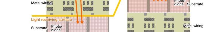

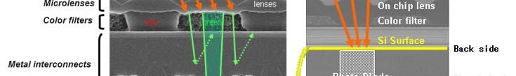
12 CMOS Image Sensor
13 MSM (Metal-Semiconductor Metal) PD Carrier collection by lateral E-field provided by Schottky contacts Not very efficient but can be very fast
14 Avalanche Photodiode (APD): PIN PD + Gain (avalanche: a large mass of snow, ice, earth, rock, or other material in swift motion down a mountainside) id Achieve gain by multiplying electrons and/or holes. Impact Ionization: Under high E-field, electrons and holes can have sufficiently high kinetic energies breaking bonds and creating new e-h pairs. E E e h + E c e E v n + p Avalanche region š h +
15 In real APD, care is taken so that only one type of carrier (either electron or hole) causes impact ionization. APD has limited application for optical communication since high-performance EDFA is easily available APD is very useful for optical interconnect applications.
Photodetector. Prof. Woo-Young Choi. Silicon Photonics (2012/2) Photodetection: Absorption => Current Generation. Currents
 Photodetection: Absorption => Current Generation. Currents") Photodetection: Absorption => Current Generation h Currents Materials for photodetection: E g < h Various methods for generating currents with photo-generated carriers: photoconductors, photodiodes, avalanche
Photodetection: Absorption => Current Generation h Currents Materials for photodetection: E g < h Various methods for generating currents with photo-generated carriers: photoconductors, photodiodes, avalanche
Lect. 10: Photodetectors
 Photodetection: Absorption => Current Generation h Currents Materials for photodetection: E g < h Various methods for generating currents with photo-generated carriers: photoconductors, photodiodes, avalanche
Lecture 12. Semiconductor Detectors - Photodetectors
 Lecture 12 Semiconductor Detectors - Photodetectors Principle of the pn junction photodiode Absorption coefficient and photodiode materials Properties of semiconductor detectors The pin photodiodes Avalanche
Chapter 4. Photodetectors
 Chapter 4 Photodetectors Types of photodetectors: Photoconductos Photovoltaic Photodiodes Avalanche photodiodes (APDs) Resonant-cavity photodiodes MSM detectors In telecom we mainly use PINs and APDs.
LEC E T C U T R U E R E 17 -Photodetectors
 LECTURE 17 -Photodetectors Topics to be covered Photodetectors PIN photodiode Avalanche Photodiode Photodetectors Principle of the p-n junction Photodiode A generic photodiode. Photodetectors Principle
Photosynthesis & Solar Power Harvesting
 Lecture 23 Semiconductor Detectors - Photodetectors Principle of the pn junction photodiode Absorption coefficient and photodiode materials Properties of semiconductor detectors The pin photodiodes Avalanche
OPTI510R: Photonics. Khanh Kieu College of Optical Sciences, University of Arizona Meinel building R.626
 OPTI510R: Photonics Khanh Kieu College of Optical Sciences, University of Arizona kkieu@optics.arizona.edu Meinel building R.626 Announcements Homework #6 is assigned, due May 1 st Final exam May 8, 10:30-12:30pm
Photodetectors Read: Kasip, Chapter 5 Yariv, Chapter 11 Class Handout. ECE 162C Lecture #13 Prof. John Bowers
 Photodetectors Read: Kasip, Chapter 5 Yariv, Chapter 11 Class Handout ECE 162C Lecture #13 Prof. John Bowers Definitions Quantum efficiency η: Ratio of the number of electrons collected to the number of
ECEN 5645 Introduc0on to Optoelectronics Class Mee0ng 25. Non- PIN Solid State Detectors
 ECEN 5645 Introduc0on to Optoelectronics Class Mee0ng 25 Non- PIN Solid State Detectors Today s Topics Avalanche Photodiodes Problem 5.6 APD Numerics and Examples Heterojunc0on Detectors Problem 5.10 Quantum
Photonic Communications Engineering Lecture. Dr. Demetris Geddis Department of Engineering Norfolk State University
 Photonic Communications Engineering Lecture Dr. Demetris Geddis Department of Engineering Norfolk State University Light Detectors How does this detector work? Image from visionweb.com Responds to range
Course overview. Me: Dr Luke Wilson. The course: Physics and applications of semiconductors. Office: E17 open door policy
 Course overview Me: Dr Luke Wilson Office: E17 open door policy email: luke.wilson@sheffield.ac.uk The course: Physics and applications of semiconductors 10 lectures aim is to allow time for at least one
MTLE-6120: Advanced Electronic Properties of Materials. Semiconductor p-n junction diodes. Reading: Kasap ,
 MTLE-6120: Advanced Electronic Properties of Materials 1 Semiconductor p-n junction diodes Reading: Kasap 6.1-6.5, 6.9-6.12 Metal-semiconductor contact potential 2 p-type n-type p-type n-type Same semiconductor
Electron Energy, E E = 0. Free electron. 3s Band 2p Band Overlapping energy bands. 3p 3s 2p 2s. 2s Band. Electrons. 1s ATOM SOLID.
 Electron Energy, E Free electron Vacuum level 3p 3s 2p 2s 2s Band 3s Band 2p Band Overlapping energy bands Electrons E = 0 1s ATOM 1s SOLID In a metal the various energy bands overlap to give a single
Single Photon detectors
 Single Photon detectors Outline Motivation for single photon detection Semiconductor; general knowledge and important background Photon detectors: internal and external photoeffect Properties of semiconductor
EE 6313 Homework Assignments
 EE 6313 Homework Assignments 1. Homework I: Chapter 1: 1.2, 1.5, 1.7, 1.10, 1.12 [Lattice constant only] (Due Sept. 1, 2009). 2. Homework II: Chapter 1, 2: 1.17, 2.1 (a, c) (k = π/a at zone edge), 2.3
Classification of Solids
 Classification of Solids Classification by conductivity, which is related to the band structure: (Filled bands are shown dark; D(E) = Density of states) Class Electron Density Density of States D(E) Examples
EE 5344 Introduction to MEMS CHAPTER 5 Radiation Sensors
 EE 5344 Introduction to MEMS CHAPTER 5 Radiation Sensors 5. Radiation Microsensors Radiation µ-sensors convert incident radiant signals into standard electrical out put signals. Radiant Signals Classification
Lecture 8. Equations of State, Equilibrium and Einstein Relationships and Generation/Recombination
 Lecture 8 Equations of State, Equilibrium and Einstein Relationships and Generation/Recombination Reading: (Cont d) Notes and Anderson 2 sections 3.4-3.11 Energy Equilibrium Concept Consider a non-uniformly
Photodiodes and other semiconductor devices
 Photodiodes and other semiconductor devices Chem 243 Winter 2017 What is a semiconductor? no e - Empty e levels Conduction Band a few e - Empty e levels Filled e levels Filled e levels lots of e - Empty
Lecture 15: Optoelectronic devices: Introduction
 Lecture 15: Optoelectronic devices: Introduction Contents 1 Optical absorption 1 1.1 Absorption coefficient....................... 2 2 Optical recombination 5 3 Recombination and carrier lifetime 6 3.1
Auxiliaire d enseignement Nicolas Ayotte
 2012-02-15 GEL 4203 / GEL 7041 OPTOÉLECTRONIQUE Auxiliaire d enseignement Nicolas Ayotte GEL 4203 / GEL 7041 Optoélectronique VI PN JUNCTION The density of charge sign Fixed charge density remaining 2
1 Name: Student number: DEPARTMENT OF PHYSICS AND PHYSICAL OCEANOGRAPHY MEMORIAL UNIVERSITY OF NEWFOUNDLAND. Fall :00-11:00
 1 Name: DEPARTMENT OF PHYSICS AND PHYSICAL OCEANOGRAPHY MEMORIAL UNIVERSITY OF NEWFOUNDLAND Final Exam Physics 3000 December 11, 2012 Fall 2012 9:00-11:00 INSTRUCTIONS: 1. Answer all seven (7) questions.
8 Photo detectors. 8.1 Detector characteristics Responsivity R
 A photo detector is a device that converts the incident optical energy in a measurable signal, e.g., a voltage signal or an electric current. Photo detectors can be subdivided into two main classes: Photon
3.1 Introduction to Semiconductors. Y. Baghzouz ECE Department UNLV
 3.1 Introduction to Semiconductors Y. Baghzouz ECE Department UNLV Introduction In this lecture, we will cover the basic aspects of semiconductor materials, and the physical mechanisms which are at the
SEMICONDUCTOR PHYSICS REVIEW BONDS,
 SEMICONDUCTOR PHYSICS REVIEW BONDS, BANDS, EFFECTIVE MASS, DRIFT, DIFFUSION, GENERATION, RECOMBINATION February 3, 2011 The University of Toledo, Department of Physics and Astronomy SSARE, PVIC Principles
Chemistry Instrumental Analysis Lecture 8. Chem 4631
 Chemistry 4631 Instrumental Analysis Lecture 8 UV to IR Components of Optical Basic components of spectroscopic instruments: stable source of radiant energy transparent container to hold sample device
Carrier Recombination
 Notes for ECE-606: Spring 013 Carrier Recombination Professor Mark Lundstrom Electrical and Computer Engineering Purdue University, West Lafayette, IN USA lundstro@purdue.edu /19/13 1 carrier recombination-generation
3.1 Absorption and Transparency
 3.1 Absorption and Transparency 3.1.1 Optical Devices (definitions) 3.1.2 Photon and Semiconductor Interactions 3.1.3 Photon Intensity 3.1.4 Absorption 3.1 Absorption and Transparency Objective 1: Recall
Phys 4061 Lecture Thirteen Photodetectors
 Phys 4061 Lecture Thirteen Photodetectors Recall properties of indirect band gap materials that are used as photodetectors Photoelectric Effect in Semiconductors hν > Eg + χ χ is the electron affinity
Spring Semester 2012 Final Exam
 Spring Semester 2012 Final Exam Note: Show your work, underline results, and always show units. Official exam time: 2.0 hours; an extension of at least 1.0 hour will be granted to anyone. Materials parameters
Direct and Indirect Semiconductor
 Direct and Indirect Semiconductor Allowed values of energy can be plotted vs. the propagation constant, k. Since the periodicity of most lattices is different in various direction, the E-k diagram must
ELEC 4700 Assignment #2
 ELEC 4700 Assignment #2 Question 1 (Kasop 4.2) Molecular Orbitals and Atomic Orbitals Consider a linear chain of four identical atoms representing a hypothetical molecule. Suppose that each atomic wavefunction
Lecture 2. Introduction to semiconductors Structures and characteristics in semiconductors
 Lecture 2 Introduction to semiconductors Structures and characteristics in semiconductors Semiconductor p-n junction Metal Oxide Silicon structure Semiconductor contact Literature Glen F. Knoll, Radiation
PHOTODETECTORS AND SILICON PHOTO MULTIPLIER
 ESE seminar Photodetectors - Sipm, P. Jarron - F. Powolny 1 PHOTODETECTORS AND SILICON PHOTO MULTIPLIER ESE seminar Pierre Jarron, Francois Powolny OUTLINE 2 Brief history and overview of photodetectors
Laser Basics. What happens when light (or photon) interact with a matter? Assume photon energy is compatible with energy transition levels.
 interact with a matter? Assume photon energy is compatible with energy transition levels.") What happens when light (or photon) interact with a matter? Assume photon energy is compatible with energy transition levels. Electron energy levels in an hydrogen atom n=5 n=4 - + n=3 n=2 13.6 = [ev]
What happens when light (or photon) interact with a matter? Assume photon energy is compatible with energy transition levels. Electron energy levels in an hydrogen atom n=5 n=4 - + n=3 n=2 13.6 = [ev]
- A free electron in CB "meets" a hole in VB: the excess energy -> a photon energy.
 5.4. Recombination and Minority Carrier Injection 5.4.1 Direct and Indirect Recombination A free electron in CB "meets" a hole in VB: the excess energy > a photon energy. Energy CB ψ cb (k cb ) ψ vb (k
EECS130 Integrated Circuit Devices
 EECS130 Integrated Circuit Devices Professor Ali Javey 8/30/2007 Semiconductor Fundamentals Lecture 2 Read: Chapters 1 and 2 Last Lecture: Energy Band Diagram Conduction band E c E g Band gap E v Valence
Sensor Technology. Summer School: Advanced Microsystems Technologies for Sensor Applications
 Sensor Technology Summer School: Universidade Federal do Rio Grande do Sul (UFRGS) Porto Alegre, Brazil July 12 th 31 st, 2009 1 Outline of the Lecture: Philosophy of Sensing Instrumentation and Systems
Chapter 1 Overview of Semiconductor Materials and Physics
 Chapter 1 Overview of Semiconductor Materials and Physics Professor Paul K. Chu Conductivity / Resistivity of Insulators, Semiconductors, and Conductors Semiconductor Elements Period II III IV V VI 2 B
Lecture 2. Introduction to semiconductors Structures and characteristics in semiconductors
 Lecture 2 Introduction to semiconductors Structures and characteristics in semiconductors Semiconductor p-n junction Metal Oxide Silicon structure Semiconductor contact Literature Glen F. Knoll, Radiation
Schottky Diodes (M-S Contacts)
") Schottky Diodes (M-S Contacts) Three MITs of the Day Band diagrams for ohmic and rectifying Schottky contacts Similarity to and difference from bipolar junctions on electrostatic and IV characteristics.
Schottky Diodes (M-S Contacts) Three MITs of the Day Band diagrams for ohmic and rectifying Schottky contacts Similarity to and difference from bipolar junctions on electrostatic and IV characteristics.
Theory of Electrical Characterization of Semiconductors
 Theory of Electrical Characterization of Semiconductors P. Stallinga Universidade do Algarve U.C.E.H. A.D.E.E.C. OptoElectronics SELOA Summer School May 2000, Bologna (It) Overview Devices: bulk Schottky
Semiconductor Fundamentals. Professor Chee Hing Tan
 Semiconductor Fundamentals Professor Chee Hing Tan c.h.tan@sheffield.ac.uk Why use semiconductor? Microprocessor Transistors are used in logic circuits that are compact, low power consumption and affordable.
Sample Exam # 2 ECEN 3320 Fall 2013 Semiconductor Devices October 28, 2013 Due November 4, 2013
 Sample Exam # 2 ECEN 3320 Fall 203 Semiconductor Devices October 28, 203 Due November 4, 203. Below is the capacitance-voltage curve measured from a Schottky contact made on GaAs at T 300 K. Figure : Capacitance
Metal Vapour Lasers Use vapoured metal as a gain medium Developed by W. Silfvast (1966) Two types: Ionized Metal vapour (He-Cd) Neutral Metal vapour
 Two types: Ionized Metal vapour (He-Cd) Neutral Metal vapour") Metal Vapour Lasers Use vapoured metal as a gain medium Developed by W. Silfvast (1966) Two types: Ionized Metal vapour (He-Cd) Neutral Metal vapour (Cu) All operate by vaporizing metal in container Helium
Metal Vapour Lasers Use vapoured metal as a gain medium Developed by W. Silfvast (1966) Two types: Ionized Metal vapour (He-Cd) Neutral Metal vapour (Cu) All operate by vaporizing metal in container Helium
Carriers Concentration and Current in Semiconductors
 Carriers Concentration and Current in Semiconductors Carrier Transport Two driving forces for carrier transport: electric field and spatial variation of the carrier concentration. Both driving forces lead
The pn junction. [Fonstad, Ghione]
![The pn junction. [Fonstad, Ghione]](/thumbs/93/112370833.jpg "The pn junction. [Fonstad, Ghione]") The pn junction [Fonstad, Ghione] Band diagram On the vertical axis: potential energy of the electrons On the horizontal axis: now there is nothing: later we ll put the position qf s : work function (F
The pn junction [Fonstad, Ghione] Band diagram On the vertical axis: potential energy of the electrons On the horizontal axis: now there is nothing: later we ll put the position qf s : work function (F
Semiconductor-Detectors
 Semiconductor-Detectors 1 Motivation ~ 195: Discovery that pn-- junctions can be used to detect particles. Semiconductor detectors used for energy measurements ( Germanium) Since ~ 3 years: Semiconductor
UNIT I: Electronic Materials.
 SIDDHARTH INSTITUTE OF ENGINEERING & TECHNOLOGY :: PUTTUR Siddharth Nagar, Narayanavanam Road 517583 QUESTION BANK (DESCRIPTIVE) Subject with Code: SEMICONDUCTOR PHYSICS (18HS0851) Course & Branch: B.Tech
(b) Spontaneous emission. Absorption, spontaneous (random photon) emission and stimulated emission.
 Spontaneous emission. Absorption, spontaneous (random photon) emission and stimulated emission.") Lecture 10 Stimulated Emission Devices Lasers Stimulated emission and light amplification Einstein coefficients Optical fiber amplifiers Gas laser and He-Ne Laser The output spectrum of a gas laser Laser
Lecture 10 Stimulated Emission Devices Lasers Stimulated emission and light amplification Einstein coefficients Optical fiber amplifiers Gas laser and He-Ne Laser The output spectrum of a gas laser Laser
Lecture 18. New gas detectors Solid state trackers
 Lecture 18 New gas detectors Solid state trackers Time projection Chamber Full 3-D track reconstruction x-y from wires and segmented cathode of MWPC z from drift time de/dx information (extra) Drift over
COURSE OUTLINE. Introduction Signals and Noise Filtering Sensors: PD5 Avalanche PhotoDiodes. Sensors, Signals and Noise 1
 Sensors, Signals and Noise 1 COURSE OUTLINE Introduction Signals and Noise Filtering Sensors: PD5 Avalanche PhotoDiodes Avalanche Photo-Diodes (APD) 2 Impact ionization in semiconductors Linear amplification
Solar cells operation
 Solar cells operation photovoltaic effect light and dark V characteristics effect of intensity effect of temperature efficiency efficency losses reflection recombination carrier collection and quantum
Purpose: To convert the received optical signal into an electrical lsignal.
 OPTICAL DETECTORS Optical Detectors Purpose: To convert the received optical signal into an electrical lsignal. Requirements For Detector HIGH SENSITIVITY (at operating wave lengths) at normal op. temp
EE 472 Solutions to some chapter 4 problems
 EE 472 Solutions to some chapter 4 problems 4.4. Erbium doped fiber amplifier An EDFA is pumped at 1480 nm. N1 and N2 are the concentrations of Er 3+ at the levels E 1 and E 2 respectively as shown in
B12: Semiconductor Devices
 B12: Semiconductor Devices Example Sheet 2: Solutions Question 1 To get from eq. (5.70) of the notes to the expression given in the examples sheet, we simply invoke the relations n 0 p 0, n 0 n 0. In this
Basic Principles of Light Emission in Semiconductors
 Basic Principles of Light Emission in Semiconductors Class: Integrated Photonic Devices Time: Fri. 8:00am ~ 11:00am. Classroom: 資電 06 Lecturer: Prof. 李明昌 (Ming-Chang Lee) Model for Light Generation and
ENERGY BANDS AND GAPS IN SEMICONDUCTOR. Muhammad Hafeez Javed
 ENERGY BANDS AND GAPS IN SEMICONDUCTOR Muhammad Hafeez Javed www.rmhjaved.com rmhjaved@gmail.com Out Line Introduction Energy band Classification of materials Direct and indirect band gap of SC Classification
Semiconductor device structures are traditionally divided into homojunction devices
 0. Introduction: Semiconductor device structures are traditionally divided into homojunction devices (devices consisting of only one type of semiconductor material) and heterojunction devices (consisting
Basic cell design. Si cell
 Basic cell design Si cell 1 Concepts needed to describe photovoltaic device 1. energy bands in semiconductors: from bonds to bands 2. free carriers: holes and electrons, doping 3. electron and hole current:
Fundamentals of Photovoltaics: C1 Problems. R.Treharne, K. Durose, J. Major, T. Veal, V.
 Fundamentals of Photovoltaics: C1 Problems R.Treharne, K. Durose, J. Major, T. Veal, V. Dhanak @cdtpv November 3, 2015 These problems will be highly relevant to the exam that you will sit very shortly.
Lecture Notes 2 Charge-Coupled Devices (CCDs) Part I. Basic CCD Operation CCD Image Sensor Architectures Static and Dynamic Analysis
 Part I. Basic CCD Operation CCD Image Sensor Architectures Static and Dynamic Analysis") Lecture Notes 2 Charge-Coupled Devices (CCDs) Part I Basic CCD Operation CCD Image Sensor Architectures Static and Dynamic Analysis Charge Well Capacity Buried channel CCD Transfer Efficiency Readout Speed
Lecture Notes 2 Charge-Coupled Devices (CCDs) Part I Basic CCD Operation CCD Image Sensor Architectures Static and Dynamic Analysis Charge Well Capacity Buried channel CCD Transfer Efficiency Readout Speed
Session 5: Solid State Physics. Charge Mobility Drift Diffusion Recombination-Generation
 Session 5: Solid State Physics Charge Mobility Drift Diffusion Recombination-Generation 1 Outline A B C D E F G H I J 2 Mobile Charge Carriers in Semiconductors Three primary types of carrier action occur
Session 6: Solid State Physics. Diode
 Session 6: Solid State Physics Diode 1 Outline A B C D E F G H I J 2 Definitions / Assumptions Homojunction: the junction is between two regions of the same material Heterojunction: the junction is between
!"#$%&'()%*&+,-.&*&',/"*"%*&+0!
%*&+,-.&*&',/*%*&+0!") "#$%&'()%*&+-.&*&'/"*"%*&+0 1.23*"+45"#$%&'()%*&+-.&*&'/"*"%*&+0 "#$"%&'(')*(*+('-.$ /0(*12321)41(*123%&'('*5*+(- 6$ 7*1*23%'8*9*- "#$:%&'('+'1);+('-.$ 41(
"#$%&'()%*&+-.&*&'/"*"%*&+0 1.23*"+45"#$%&'()%*&+-.&*&'/"*"%*&+0 "#$"%&'(')*(*+('-.$ /0(*12321)41(*123%&'('*5*+(- 6$ 7*1*23%'8*9*- "#$:%&'('+'1);+('-.$ 41(
PHOTOVOLTAICS Fundamentals
 PHOTOVOLTAICS Fundamentals PV FUNDAMENTALS Semiconductor basics pn junction Solar cell operation Design of silicon solar cell SEMICONDUCTOR BASICS Allowed energy bands Valence and conduction band Fermi
Solid State Physics SEMICONDUCTORS - IV. Lecture 25. A.H. Harker. Physics and Astronomy UCL
 Solid State Physics SEMICONDUCTORS - IV Lecture 25 A.H. Harker Physics and Astronomy UCL 9.9 Carrier diffusion and recombination Suppose we have a p-type semiconductor, i.e. n h >> n e. (1) Create a local
Stimulated Emission Devices: LASERS
 Stimulated Emission Devices: LASERS 1. Stimulated Emission and Photon Amplification E 2 E 2 E 2 hυ hυ hυ In hυ Out hυ E 1 E 1 E 1 (a) Absorption (b) Spontaneous emission (c) Stimulated emission The Principle
Outline. Photosensors in biology and in semiconductors. The visual pathway Bottom view. The visual pathway Side view
 Outline Photosensors in biology and in semiconductors CNS WS07-08 Class 1 Photosensors in biology The visual pathway and the retina Photoreceptors and the fovea Giacomo Indiveri Institute of Neuroinformatics
EECS143 Microfabrication Technology
 EECS143 Microfabrication Technology Professor Ali Javey Introduction to Materials Lecture 1 Evolution of Devices Yesterday s Transistor (1947) Today s Transistor (2006) Why Semiconductors? Conductors e.g
ECE 250 Electronic Devices 1. Electronic Device Modeling
 ECE 250 Electronic Devices 1 ECE 250 Electronic Device Modeling ECE 250 Electronic Devices 2 Introduction to Semiconductor Physics You should really take a semiconductor device physics course. We can only
Designing Information Devices and Systems II A. Sahai, J. Roychowdhury, K. Pister Discussion 1A
 EECS 16B Spring 2019 Designing Information Devices and Systems II A. Sahai, J. Roychowdhury, K. Pister Discussion 1A 1 Semiconductor Physics Generally, semiconductors are crystalline solids bonded into
External (differential) quantum efficiency Number of additional photons emitted / number of additional electrons injected
 quantum efficiency Number of additional photons emitted / number of additional electrons injected") Semiconductor Lasers Comparison with LEDs The light emitted by a laser is generally more directional, more intense and has a narrower frequency distribution than light from an LED. The external efficiency
Semiconductor Lasers Comparison with LEDs The light emitted by a laser is generally more directional, more intense and has a narrower frequency distribution than light from an LED. The external efficiency
Temperature and Silicon Film Thickness Influence on the Operation of Lateral SOI PIN Photodiodes for Detection of Short Wavelengths
 04 (51)-AF:Modelo-AF 8/20/11 6:37 AM Page 107 Temperature and Silicon Film Thickness Influence on the Operation of Lateral SOI PIN Photodiodes for Detection of Short Wavelengths Michelly de Souza 1, Olivier
Chapter 7. Solar Cell
 Chapter 7 Solar Cell 7.0 Introduction Solar cells are useful for both space and terrestrial application. Solar cells furnish the long duration power supply for satellites. It converts sunlight directly
Semiconductor Physics and Devices Chapter 3.
 Introduction to the Quantum Theory of Solids We applied quantum mechanics and Schrödinger s equation to determine the behavior of electrons in a potential. Important findings Semiconductor Physics and
UNIT - IV SEMICONDUCTORS AND MAGNETIC MATERIALS
 1. What is intrinsic If a semiconductor is sufficiently pure, then it is known as intrinsic semiconductor. ex:: pure Ge, pure Si 2. Mention the expression for intrinsic carrier concentration of intrinsic
Engineering 2000 Chapter 8 Semiconductors. ENG2000: R.I. Hornsey Semi: 1
 Engineering 2000 Chapter 8 Semiconductors ENG2000: R.I. Hornsey Semi: 1 Overview We need to know the electrical properties of Si To do this, we must also draw on some of the physical properties and we
Uniform excitation: applied field and optical generation. Non-uniform doping/excitation: diffusion, continuity
 6.012 - Electronic Devices and Circuits Lecture 2 - Uniform Excitation; Non-uniform conditions Announcements Review Carrier concentrations in TE given the doping level What happens above and below room
Fall 2014 Nobby Kobayashi (Based on the notes by E.D.H Green and E.L Allen, SJSU) 1.0 Learning Objectives
 1.0 Learning Objectives") University of California at Santa Cruz Electrical Engineering Department EE-145L: Properties of Materials Laboratory Lab 7: Optical Absorption, Photoluminescence Fall 2014 Nobby Kobayashi (Based on the
University of California at Santa Cruz Electrical Engineering Department EE-145L: Properties of Materials Laboratory Lab 7: Optical Absorption, Photoluminescence Fall 2014 Nobby Kobayashi (Based on the
Schottky Rectifiers Zheng Yang (ERF 3017,
 ECE442 Power Semiconductor Devices and Integrated Circuits Schottky Rectifiers Zheng Yang (ERF 3017, email: yangzhen@uic.edu) Power Schottky Rectifier Structure 2 Metal-Semiconductor Contact The work function
Structural Optimization of Silicon Carbide PIN Avalanche Photodiodes for UV Detection
 Journal of the Korean Physical Society, Vol. 56, No. 2, February 2010, pp. 672 676 Structural Optimization of Silicon Carbide PIN Avalanche Photodiodes for UV Detection Ho-Young Cha School of Electronic
Supporting Information. InGaAs Nanomembrane/Si van der Waals Heterojunction. Photodiodes with Broadband and High Photoresponsivity
 Supporting Information InGaAs Nanomembrane/Si van der Waals Heterojunction Photodiodes with Broadband and High Photoresponsivity Doo-Seung Um, Youngsu Lee, Seongdong Lim, Jonghwa Park, Wen-Chun Yen, Yu-Lun
Lecture 4 - Carrier generation and recombination. February 12, 2007
 6.720J/3.43J - Integrated Microelectronic Devices - Spring 2007 Lecture 4-1 Contents: Lecture 4 - Carrier generation and recombination 1. G&R mechanisms February 12, 2007 2. Thermal equilibrium: principle
Studying of the Dipole Characteristic of THz from Photoconductors
 PIERS ONLINE, VOL. 4, NO. 3, 8 386 Studying of the Dipole Characteristic of THz from Photoconductors Hong Liu, Weili Ji, and Wei Shi School of Automation and Information Engineering, Xi an University of
collisions of electrons. In semiconductor, in certain temperature ranges the conductivity increases rapidly by increasing temperature
 1.9. Temperature Dependence of Semiconductor Conductivity Such dependence is one most important in semiconductor. In metals, Conductivity decreases by increasing temperature due to greater frequency of
Electronic Devices & Circuits
 Electronic Devices & Circuits For Electronics & Communication Engineering By www.thegateacademy.com Syllabus Syllabus for Electronic Devices Energy Bands in Intrinsic and Extrinsic Silicon, Carrier Transport,
EE 446/646 Photovoltaic Devices I. Y. Baghzouz
 EE 446/646 Photovoltaic Devices I Y. Baghzouz What is Photovoltaics? First used in about 1890, the word has two parts: photo, derived from the Greek word for light, volt, relating to electricity pioneer
Section 12: Intro to Devices
 Section 12: Intro to Devices Extensive reading materials on reserve, including Robert F. Pierret, Semiconductor Device Fundamentals EE143 Ali Javey Bond Model of Electrons and Holes Si Si Si Si Si Si Si
Effective masses in semiconductors
 Effective masses in semiconductors The effective mass is defined as: In a solid, the electron (hole) effective mass represents how electrons move in an applied field. The effective mass reflects the inverse
An Ensemble Monte Carlo Model to Calculate Photocurrent of MSM Photodetector
 www.ijcsi.org 319 An Ensemble Monte Carlo Model to Calculate Photocurrent of MSM Photodetector M. Soroosh 1 and Y. Amiri 2 1 Department of Electrical and Computer Engineering, Shahid Chamran University,
Chapter 5. Semiconductor Laser
 Chapter 5 Semiconductor Laser 5.0 Introduction Laser is an acronym for light amplification by stimulated emission of radiation. Albert Einstein in 1917 showed that the process of stimulated emission must
Paper Review. Special Topics in Optical Engineering II (15/1) Minkyu Kim. IEEE Journal of Quantum Electronics, Feb 1985
 Minkyu Kim. IEEE Journal of Quantum Electronics, Feb 1985") Paper Review IEEE Journal of Quantum Electronics, Feb 1985 Contents Semiconductor laser review High speed semiconductor laser Parasitic elements limitations Intermodulation products Intensity noise Large
Paper Review IEEE Journal of Quantum Electronics, Feb 1985 Contents Semiconductor laser review High speed semiconductor laser Parasitic elements limitations Intermodulation products Intensity noise Large
p-n junction biasing, p-n I-V characteristics, p-n currents Norlaili Mohd. Noh EEE /09
 CLASS 6&7 p-n junction biasing, p-n I-V characteristics, p-n currents 1 p-n junction biasing Unbiased p-n junction: the potential barrier is 0.7 V for Si and 0.3 V for Ge. Nett current across the p-n junction
Astronomical Observing Techniques 2017 Lecture 9: Silicon Eyes 1
 Astronomical Observing Techniques 2017 Lecture 9: Silicon Eyes 1 Christoph U. Keller keller@strw.leidenuniv.nl Content 1. Detector Types 2. Crystal La>ces 3. Electronic Bands 4. Fermi Energy and Fermi
Photodetectors and their Spectral Ranges
 Photodetectors and their Spectral Ranges SINGLE ELEMENT IMAGE - photoemission devices vacuum photodiode pickup tubes (or external gas photodiode image intensifiers photoelectric devices) photomultiplier
Photovoltaic cell and module physics and technology. Vitezslav Benda, Prof Czech Technical University in Prague
 Photovoltaic cell and module physics and technology Vitezslav Benda, Prof Czech Technical University in Prague benda@fel.cvut.cz www.fel.cvut.cz 1 Outlines Photovoltaic Effect Photovoltaic cell structure
Appendix 1: List of symbols
 Appendix 1: List of symbols Symbol Description MKS Units a Acceleration m/s 2 a 0 Bohr radius m A Area m 2 A* Richardson constant m/s A C Collector area m 2 A E Emitter area m 2 b Bimolecular recombination
Introduction. Katarzyna Skorupska. Silicon will be used as the model material however presented knowledge applies to other semiconducting materials
 Introduction Katarzyna Skorupska Silicon will be used as the model material however presented knowledge applies to other semiconducting materials 2 June 26 Intrinsic and Doped Semiconductors 3 July 3 Optical
SEMICONDUCTOR PHYSICS
 SEMICONDUCTOR PHYSICS by Dibyendu Chowdhury Semiconductors The materials whose electrical conductivity lies between those of conductors and insulators, are known as semiconductors. Silicon Germanium Cadmium