Oxidation. Reading Assignments: Plummer, Chap 6.1~6.4, 6.5.1, 6.5.3, 6.5.4, 6.5.5,
|
|
|
- Basil Richards
- 6 years ago
- Views:
Transcription
1 Oxidation Reading Assignments: Plummer, Chap 6.1~6.4, 6.5.1, 6.5.3, 6.5.4, 6.5.5,
2 Why SiO 2? The extraordinary properties of SiO 2 are the basis of the success of MOS-technology Non-crystalline insulator Very high energy gap Φ M Easy to grow on Si Easy to integrate in a process E M Excellent interface between Si substrate Stable and insensitive to following process-steps Excellent scaling possibilities no real candidates for replacement E 0 1.0eV χ ox 9.0eV 3.0eV 4.9eV Φ S χ si E C E V 2
 Dielectric constant: 3.9 Energy gap : 9 ev Density : 2.20 g/cm 3 Refractive Index : ~1.")
3 Properties of SiO 2 Si-Si : 3.12 Å, Si-O: 1.62 Å, O-O: 2.27 Å 10 nm : atomic layers 1.2 nm : only about 4 atomic layers Bonding angle : 110~180 ( 144 ) Dielectric constant: 3.9 Energy gap : 9 ev Density : 2.20 g/cm 3 Refractive Index : ~1.462 Dielectric strength MV/cm Tetrahedra structure θ Bridging Oxygen Oxygen Silicon 3

4 Application of Thermal Oxides 4
5 Transistor Process Flow (1970s) Al Si nmos Cross-section PSG poly n + n + p-si SiN Clean p-si p-si Field Oxidation Oxide Etch p-si p-si Gate Oxidation Poly Dep. p-si poly p-si poly Poly Etch P + Ion Implant p-si poly n + poly p-si n + Annealing 5
6 Masking Oxide Much lower B and P diffusion rates in SiO 2 than that in Si SiO 2 can be used as diffusion mask Dopant SiO 2 SiO 2 Si 6
7 Pad Oxide Relieve strong tensile stress of the nitride Prevent stress induced silicon defects Silicon nitride Pad Oxide Silicon Substrate 7
8 Blanket Field Oxide Isolation Silicon Wafer Clean Silicon Dioxide Silicon Activation Area Field Oxidation Field Oxide Silicon Oxide Etch 8
 E BD > 8MV/cm, pinhole free and negligible defects Sufficient long lifetime under normal operating High resistance to hot-carrier")
9 Gate Oxide Thickness of oxide (T ox ) must closely match the specification of the MOSFET design T ox must be sufficiently uniform across the entire wafer, and from wafer to wafer, and from run-to-run Extremely low Q f and D it (Good Si/SiO 2 interfacial properties) E BD > 8MV/cm, pinhole free and negligible defects Sufficient long lifetime under normal operating High resistance to hot-carrier damage Resistance to boron penetration Refer to Dr. Hong Xiao V G V D > 0 Poly Si Gate Thin oxide n + Source Electrons p-si n + Drain Si Substrate Source: Dr. PT Liu 9
10 Growth Mechanism Native oxide: Si surface has a high affinity for oxygen formed in the air or chemical cleaning process quality is bad and should be eliminated Å Thermal oxidation: Dry Oxidation Si( solid) + O SiO ( solid) 2 2 Wet Oxidation (steam oxide) Si( solid) + H O SiO ( solid) + 2H
11 1000 o C Si + O 2 SiO 2 Dry Oxidation Original Silicon Surface O 2 Silicon Dioxide O 2 O 2 (SiO 2 ) O 2 O 2 O 2 O 2 O 2 O 2 O 2 O 2 O 2 O 2 O 2 55% O 2 45% Silicon wafer (Si) Thickness of silicon = 0.45 x (thickness of SiO 2 ) Si substrate Si substrate Oxidizing species diffuse through SiO 2 to Si/SiO 2 Source: Dr. PT Liu 11
12 Silicon nitride LOCOS Process Pad Oxide P-type substrate Pad oxidation, nitride deposition and patterning Silicon nitride SiO 2 p + P-type substrate p + Isolation Doping p + LOCOS oxidation SiO 2 p + P-type substrate p + Isolation Doping p + Nitride and pad oxide strip Bird s Beak 12

13 Typical LOCOS and Bird s Beak Deposited Polysilicon Volume Expansion SiO 2 Original Si Surface Location of Si 3 N 4 Mask Si Substrate 13
14 LOCOS Compare with blanket field oxide Better isolation Lower step height Less steep sidewall Disadvantage rough surface topography Bird s beak Replacing by shallow trench isolation (STI) 14
15 Stress Mismatch between different materials Two kinds of stresses, intrinsic and extrinsic Intrinsic stress develops during the film nucleation and growth process. The extrinsic stress results from differences in the coefficients of thermal expansion Tensile stress: cracking film if too high Compressive stress: hillock if too strong 15
16 Film Stress Bare Wafer After Thin Film Deposition Substrate Substrate Compressive Stress (tend to expand) Negative curvature Substrate Tensile Stress (tend to contract) Positive curvature 16
17 Illustration of Thermal Stress SiO 2 Si At 400 C L SiO 2 Si Under compressive stress At Room Temperature ΔL = α ΔT L ΔL 17
18 Coefficients of Thermal Expansion α(sio 2 ) = C 1 α(si) = C 1 α(si 3 N 4 ) = C 1 α(w) = C 1 α(al) = C 1 18
19 Interfacial Structure Dangling bond Si Si Si Si surface SiO 2 Si Si Si Si Si Si Interfacial trap Si Si Si Si Si Si Si Si Si Si Si Si Si Si Si Si impurity Oxygen vacancy Stretched bond 19

20 Interfacial Structure bulk-oxide count TEM boundary total Oxygen count sub-oxide count t ox D. Muller, et. al, Nature, 399, 758(1999) 20
21 Oxide Traps and Defects Mobile Ionic Charge K + Na + Oxide Trapped Charge Fixed Oxide Charge Interface Trapped Charge (Deal, 1980) Fixed Charge (Q f, N f ) (Positive): structural defects due to incomplete oxidation and stress, within 2.5 nm from Si/SiO 2 not electrically communicate with interface states Mobile Oxide Charge (Q m, N m ): Na +, Li +,K +,H + Oxide Trapped Charge (Q ot,n ot ): positive or negative due to hole or electron traps in borken Si-O bonds radiation, charge injection in high field Interface Trapped Charge (Q it,n it, D it ): structural defects due to incomplete oxidation at Si/SiO 2 donor or acceptor-like surface-potential dependent 21
22 SiO 2 /Si Interface Interface states: imperfect bonds Electrically interacted with channel carriers Assuming each dangling bond give rise to one interface state Impact on device characteristics threshold voltage ( V t ) carrier mobility ( G m ) reliability, oxide integrity and HCI( hot-carrier-injection) degradation Hydrogen annealing at o C is effective to passivate Q it at the very end step of process. 22
23 Deal-Grove Triangle Q f decreases with increasing oxidation temperature Dry O 2 Post oxidation annealing in N 2 or Argon ambient is needed to minimize Q f However, annealing should be kept within specific time period without causing Dry N 2 or Argon increase of Q f Fixed Charge, Q f 23
24 Oxide Growth: Deal-Grove Model Deal-Grove Relation (linear-parabolic growth law): Linear Growth (Reaction-Limited) Regime B Oxide Thickness X = t A Diffusion-limited Regime X = B t t ox t Si 0.44 t ox Top oxide surface Original silicon surface Oxidation Time Silicon Oxide-silicon surface 24
25 <100> Silicon Dry Oxidation Oxide Thickness (micron) <100> Silicon Dry Oxidation 1200 C 1150 C 1100 C 1050 C 1000 C 950 C 900 C Oxidation Time (hours) 25
 In equilibrium, the")
26 Deal-Grove Model-1 Oxidants must be transported from the bulk of the gas to the oxide surface. F = h ( C 1 g g s C g : oxidant concentration in bulk of gas C s : oxidant concentration right next to the oxide surface h g : gas phase mass-transfer coefficient Henry s law C ) In equilibrium, the concentration of a species within a solid is proportional to the partial pressure of that species in the surrounding gas. Gas Oxide Silicon C=Hp, where H is the Henry s law constant and p is the gas pressure C d G Cs C* = H p g (equilibrium concentration in bulk SiO 2 ) C o C o = H p s (equilibrium concentration at bulk gas/sio 2 interface) For ideal gas C = p/kt C i * F1 = h( C Co ), where h = hg / HkT x F 1 F 2 F 3 26
27 Deal-Grove Model-2 Oxidants must diffuse across the oxide layer already present. F 2 C = D o C x o D is the diffusivity of oxidant in bulk oxide C i is the oxidant concentration in bulk oxide at the oxide/silicon interface x o is the thickness of oxide layer already present Oxidants must react at the oxide/silicon interface F = k C 3 s i i k s is the chemical surface-reaction rate constant C g Gas phase O 2 F 1 SiO 2 Si O 2 Concentration C 0 O 2 F 2 X 0 C* C i O 2 +Si F 3 SiO 2 27
28 Deal-Grove Model-3 Reaction control Steady state : F=F 1 =F 2 =F 3 * * C C Ci = k k x k x h D D kx s o * 1+ C D * Co = C ks ksxo 1+ + h D kx s o As 0 Ci Co D kx s o As Ci 0 D s s o s o and C g Gas phase C g Gas phase O 2 F 1 SiO 2 Si O 2 Concentration C 0 O 2 F 2 X 0 C* C i Diffusion control SiO 2 Si O 2 F 2 O 2 +Si C* F 3 C 0 SiO 2 C i O 2 +Si F 3 SiO 2 O 2 Concentration X 0 28
29 Deal-Grove Model-4 There are SiO 2 atoms in one cubic centimeter: N I N * dx k C dx B o s o = F = = I 3 dt k k x s s o dt 2x + A o 1+ + h * DC x + Ax i i A= 2 D[ + ] B= τ = k h N B s D A, B : temperature, ambient composition, pressure and crystalline orientation τ is related to the initial oxide thickness I Applying the boundary condition: x o =x i at t=0, the solution of above equation is as expressed in the next slice 29
30 Growth Mechanism Deal-Grove Relation (linear-parabolic growth law): 2 ox T + AT = B( t+ τ ) 2 Tox ox for t >> τ, t >> A 2 /4B = for (t+ τ) << A 2 /4B T ox Bt Diffusion-controlled B = ( t+τ ) A Reaction-controlled t ox A, B : temperature, ambient composition, pressure and crystalline orientation τ is related to the initial oxide thickness t Si 0.44 t ox Top oxide surface Silicon Original silicon surface Oxide-silicon surface 30
31 Effect of Temperature exponentially Oxygen diffusivity ~1.17eV Water diffusivity ~0.80eV near to Si-Si bond breaking ~ 1.83eV VLSI Technology S.M. Sze 31
32 Effect of Pressure The concentration of oxidant just inside the oxide at the gas/sio 2 interface C * is proportional to p g, then both B and B/A are proportional to p g. 32

33 Effect of Crystal Orientation Effect of crystal orientation is explained by the differences in the surface density of silicon atoms on the various crystal faces. 33
 Si atoms in")


34 Orientation Dependence <100> <110> <111> Orientation Area of unit cell (cm 2 ) Si atoms in area Si bonds in area Bonds available Bonds Available cm -2 bonds cm -2 N relative to <110> <110> 2a <111> 1/2 3a <100> a
35 Thin Oxide Growth Massoud s empirical model: dxo B = + C exp dt 2xo + A E A C = C oexp kt 8 C μm / hr, E o A xo L 2.35eV, and L 7nm Apply to either (111) or (100) oriented Si. The first term is the Deal-Grove Model. The second term represents an additional oxidation mechanism. The actual mechanism is still not clear. 35
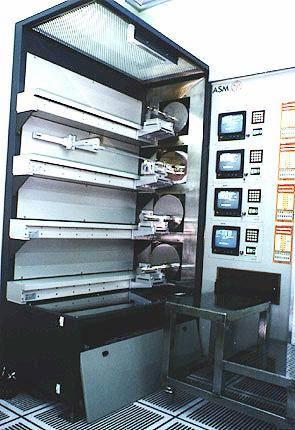
36 Conventional Furnace Equipment 36
37 Thermal Process Hardware Control System Gas Delivery System Loading System Exhaust System Process Tube 37
38 MFC Furnace System MFC MFC MFC Process Tube Control Valve Scrubber Regulator HCl O 2 N 2 吹除淨化氮氣 Exhaust Control System 在氧化製程中, 總是把氮氣當作鈍氣應用在系統閒置時 晶圓裝載 溫度提昇 溫度穩定和晶圓卸載等步驟中 乾式氧化步驟中也使用氯化氫,HCl or TCA (trichloroethane), 來減少氧化物中的移動離子, 使其成為不可移動的氯化物化合物, 並將界面電荷 (Interface state charge) 降至最低!! 38
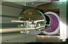
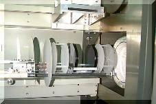
39 Furnace Configuration Horizontal Tube Vertical Tube Center Zone Heating Coils Heaters Gas Flow Quartz Tube T 1 /sec ± 0.5 Flat Zone Tower several hundred wafers Distance 39
40 Rapid Thermal Process (RTP) External Chamber Ramp Up Ramp Down Process Gas Temperature Quartz Chamber Tungsten-Halogen Lamp IR Pyrometer Time >100 o C/sec >50 o C/sec 40

41 RTP Tool Bottom Lamps Top Lamps Wafer 41
42 Dry Oxide Process Sequence Idle with purge N 2 flow Idle with process N 2 flow Wafer boat push in with process N 2 / O 2 flow Temperature ramp-up with process N 2 / O 2 flow Temperature stabilization with process N 2 / O 2 flow Oxidation with O 2, HCl; stop N 2 flow Oxide annealing; stop O 2 ; start process N 2 flow Temperature cool-down with process N 2 flow Wafer boat pull out with process N 2 flow Idle with process N 2 flow Repeat process with next boat 42
43 Oxidation Recipe 43
44 Wet Oxidation Faster, higher throughput (H 2 O, HO species) Thick oxide, such as LOCOS Dry oxide has better quality Process Temperature Thickness Oxidation Time Dry oxidation 1000 C 1000 Å ~ 2 hr Wet oxidation 1000 C 1000 Å ~ 12 min Source: Dr. PT Liu 44
45 Effect of Oxidation Ambient Wet oxidation rate is much higher than dry oxidation rate because HO - or H 2 O diffuses much faster than O 2 in SiO 2. 45
46 Pyrogenic Steam System Hydrogen Flame, 2 H 2 + O 2 2 H 2 O O 2 H 2 To Exhaust Thermal Couple Process Tube Paddle Wafer Boat Typical H 2 :O 2 ratio is between 1.8:1 to 1.9:1. 46
")
47 Outside Torch System (OTS) 47
48 Pyrogenic Wet Oxidation System MFC Process Tube MFC MFC MFC Wafers Burn Box Control Valves H 2 Process N 2 O 2 Purge N 2 Regulator Scrubbier Exhaust 48
49 Pyrogenic Oxide Process Sequence Idle with purge N 2 flow Idle with process N 2 flow Ramp O 2 with process N 2 Wafer boat push in with O 2 and process N 2 flows Temperature ramp-up with O 2 and process N 2 flows Temperature stabilization with O 2 and process N 2 flows Ramp O 2 turn off N 2 flow Stabilize O 2 flow Turn on H 2 flow, ignition, and H 2 flow stabilization 49
50 Pyrogenic Oxide Process Sequence (Cont.) Steam oxidation with O 2 and H 2 flows Hydrogen termination; turn off H 2 while keeping O 2 flow Oxygen termination; turn off O 2, start process N 2 flow Temperature ramp-down with process N 2 flow Wafer boat pull out with process N 2 flow Idle with process N 2 flow Repeat process with next boat Idle with purge N 2 flow 50
51 Oxide Measurement Thickness Uniformity SEM, TEM, Profilermeter Color chart Spectrophotometry (Reflectometry) Ellipsometry C-V I-V, breakdown voltage C-V, oxide charge 51
52 Spectrophotometry (Reflectometry) Incident light 1 Interference 2 Human eye or photodetector t Dielectric film, n( λ) Substrate 52

53 Interference in Thin Films 180 o phase change λ 0 n 0 sinφ= n 1 sinβ λ 1 = λ 0 /n 1 n 2 > n 1 > n 0 =1 λ 2nx cosβ 2x cosβ = m λ = n m m = 1,2,3 : constructive interference m = 1/ 2,3 / 2,5 / 2 : distructive interference 53
54 Color Chart 54
55 Spectroreflectometry System Substrate Film Detectors UV lamp Reflectance (%) Constructive interference Destructive interference λ 1 λ 2 λ Wavelength (nm) 55
56 Capacitance Measurement of MOS-C Small-signal capacitance MOS capacitance is defined as small signal capacitance and is measured by applying a small ac voltage on the top of a dc bias Impedance is measured by an precision impedance meter The imaginary part of the measured impedance is converted to capacitance. Superimposed AC signal 56
57 Charge Response in LFCV, HFCV and DD Accumulation ρ ac charge response dc charge response Depletion ρ Deep Depletion LFCV HFCV ρ ρ ρ Inversion W C W depl = 1 Cox = = 1 1 ε ox W C C ε t 2 qn ox si si ox ε siε0 ψ s A W dm = 2ε siε0 qn 2ψ The DC V G is swept very fast (<0.01s), the inverted minority carriers do not have time to be thermally generated. A F W dm W dm W dm 57
58 MOS CV: LFCV, HFCV and DD v ss V G Metal Oxide Si LFCV Minority carrier can follow V G and v ss Inv. C/C ox 1 Flat band will have a little smaller C depending on the size of v ss HFCV Dep. Acc. V G (quiescent point) C ox C si C si = Inverted minority carrier can follow V G but not v ss dqs dψ s deep depletion V th Minority carrier cannot follow either V G or V ss V G 58
59 Substrate Type N-type substrate (PMOS): invers. depl. 0 accumul. P-type substrate (NMOS): accumul. 0 depl. invers. V G V G C/C ox C/C ox n-type bulk (PMOS) p-type bulk (NMOS) V G V G V G V G 59
60 Oxide Thickness Determination Oxide Thickness ( T ox ) C ox is high frequency capacitance with the device biased in strong accumulation strong accumulation C H High-Frequency p-sub t ox = Aε C ox ox where A=gate area ( cm 2 ) ε ox = permittivity of oxide material ( F/cm ) C ox = oxide capacitance ( pf ) V G T ox estimated from the CV method may be slightly larger than the thickness measured by the optical method because the additonal QM correction in the accumulation layer. 60
61 Effect of Oxide Charges Flat-band voltage (V fb ) and threshold voltage (V th ) V fb Definition: The gate voltage at which the energy band in Si substrate is flat, i.e. zero field in Si. V V T ot it f fb = φms Cox Cox Cox C 0 ox th = V fb Q Q C Si ox Positive oxide charge Q + 2φ F Q 1 C/C ox ox x T ox ρ m ( x) dx K + Na + Oxide Trapped Charge Mobile Ionic Charge Fixed Oxide Charge Interface Trapped Charge 61
62 Interface Traps at One Energy Level We will first examine an ideal case: a midgap trap with donor-like behavior: when the Fermi level is above the trap level, the trap is filled and exhibits no charge (trap filled with electron); when the Fermi level is below the trap level, the trap is empty and exhibits a positive charge state (trap empty). 0 filled pmos E C E F E V + 0 partially filled E C E F E V + empty accumulation depletion inversion HFCV distorted by midgap donor-like trap pmos C/C ox midgap depletion point E C E F E V ideal HFCV 62
63 Passivation of Interface Traps If we have instead a distribution of trap levels across the band gap, then the resulting influence of HFCV will be a distortion of the ideal CV curve. Notice that how different trap types can distort CV in different ways. donor-like traps acceptorlike traps pmos E C E F E V affected by donor-like traps C/C ox affected by acceptor-like traps ideal HFCV 63
64 High-Low Frequency CV HF must be high enough so that the charge/discharge of traps cannot follow. HF must be low enough so that the charge/discharge of traps can follow. 64
Section 12: Intro to Devices
 Section 12: Intro to Devices Extensive reading materials on reserve, including Robert F. Pierret, Semiconductor Device Fundamentals Bond Model of Electrons and Holes Si Si Si Si Si Si Si Si Si Silicon
MOS CAPACITOR AND MOSFET
 EE336 Semiconductor Devices 1 MOS CAPACITOR AND MOSFET Dr. Mohammed M. Farag Ideal MOS Capacitor Semiconductor Devices Physics and Technology Chapter 5 EE336 Semiconductor Devices 2 MOS Capacitor Structure
Semiconductor Devices. C. Hu: Modern Semiconductor Devices for Integrated Circuits Chapter 5
 Semiconductor Devices C. Hu: Modern Semiconductor Devices for Integrated Circuits Chapter 5 Global leader in environmental and industrial measurement Wednesday 3.2. afternoon Tour around facilities & lecture
an introduction to Semiconductor Devices
 an introduction to Semiconductor Devices Donald A. Neamen Chapter 6 Fundamentals of the Metal-Oxide-Semiconductor Field-Effect Transistor Introduction: Chapter 6 1. MOSFET Structure 2. MOS Capacitor -
Section 12: Intro to Devices
 Section 12: Intro to Devices Extensive reading materials on reserve, including Robert F. Pierret, Semiconductor Device Fundamentals EE143 Ali Javey Bond Model of Electrons and Holes Si Si Si Si Si Si Si
ESE 570: Digital Integrated Circuits and VLSI Fundamentals
 ESE 570: Digital Integrated Circuits and VLSI Fundamentals Lec 4: January 23, 2018 MOS Transistor Theory, MOS Model Penn ESE 570 Spring 2018 Khanna Lecture Outline! CMOS Process Enhancements! Semiconductor
Fabrication Technology, Part I
 EEL5225: Principles of MEMS Transducers (Fall 2004) Fabrication Technology, Part I Agenda: Microfabrication Overview Basic semiconductor devices Materials Key processes Oxidation Thin-film Deposition Reading:
EE 560 MOS TRANSISTOR THEORY
 1 EE 560 MOS TRANSISTOR THEORY PART 1 TWO TERMINAL MOS STRUCTURE V G (GATE VOLTAGE) 2 GATE OXIDE SiO 2 SUBSTRATE p-type doped Si (N A = 10 15 to 10 16 cm -3 ) t ox V B (SUBSTRATE VOLTAGE) EQUILIBRIUM:
ESE 570: Digital Integrated Circuits and VLSI Fundamentals
 ESE 570: Digital Integrated Circuits and VLSI Fundamentals Lec 4: January 29, 2019 MOS Transistor Theory, MOS Model Penn ESE 570 Spring 2019 Khanna Lecture Outline! CMOS Process Enhancements! Semiconductor
Thermal Oxidation of Si
 Thermal Oxidation of General Properties of O 2 Applications of thermal O 2 Deal-Grove Model of Oxidation Thermal O 2 is amorphous. Weight Density = 2.20 gm/cm 3 Molecular Density = 2.3E22 molecules/cm
Lecture 12: MOS Capacitors, transistors. Context
 Lecture 12: MOS Capacitors, transistors Context In the last lecture, we discussed PN diodes, and the depletion layer into semiconductor surfaces. Small signal models In this lecture, we will apply those
FIELD-EFFECT TRANSISTORS
 FIEL-EFFECT TRANSISTORS 1 Semiconductor review 2 The MOS capacitor 2 The enhancement-type N-MOS transistor 3 I-V characteristics of enhancement MOSFETS 4 The output characteristic of the MOSFET in saturation
Chapter 3 Basics Semiconductor Devices and Processing
 Chapter 3 Basics Semiconductor Devices and Processing Hong Xiao, Ph. D. www2.austin.cc.tx.us/hongxiao/book.htm Hong Xiao, Ph. D. www2.austin.cc.tx.us/hongxiao/book.htm 1 Objectives Identify at least two
ECE 340 Lecture 39 : MOS Capacitor II
 ECE 340 Lecture 39 : MOS Capacitor II Class Outline: Effects of Real Surfaces Threshold Voltage MOS Capacitance-Voltage Analysis Things you should know when you leave Key Questions What are the effects
MOSFET: Introduction
 E&CE 437 Integrated VLSI Systems MOS Transistor 1 of 30 MOSFET: Introduction Metal oxide semiconductor field effect transistor (MOSFET) or MOS is widely used for implementing digital designs Its major
Self-study problems and questions Processing and Device Technology, FFF110/FYSD13
 Self-study problems and questions Processing and Device Technology, FFF110/FYSD13 Version 2016_01 In addition to the problems discussed at the seminars and at the lectures, you can use this set of problems
ESE 570: Digital Integrated Circuits and VLSI Fundamentals
 ESE 570: Digital Integrated Circuits and VLSI Fundamentals Lec 4: January 24, 2017 MOS Transistor Theory, MOS Model Penn ESE 570 Spring 2017 Khanna Lecture Outline! Semiconductor Physics " Band gaps "
Fundamentals of the Metal Oxide Semiconductor Field-Effect Transistor
 Triode Working FET Fundamentals of the Metal Oxide Semiconductor Field-Effect Transistor The characteristics of energy bands as a function of applied voltage. Surface inversion. The expression for the
Quiz #1 Practice Problem Set
 Name: Student Number: ELEC 3908 Physical Electronics Quiz #1 Practice Problem Set? Minutes January 22, 2016 - No aids except a non-programmable calculator - All questions must be answered - All questions
EE-612: Lecture 22: CMOS Process Steps
 EE-612: Lecture 22: CMOS Process Steps Mark Lundstrom Electrical and Computer Engineering Purdue University West Lafayette, IN USA Fall 2006 NCN www.nanohub.org Lundstrom EE-612 F06 1 outline 1) Unit Process
Lecture 2. Introduction to semiconductors Structures and characteristics in semiconductors
 Lecture 2 Introduction to semiconductors Structures and characteristics in semiconductors Semiconductor p-n junction Metal Oxide Silicon structure Semiconductor contact Literature Glen F. Knoll, Radiation
Fabrication and Characterization of Al/Al2O3/p-Si MOS Capacitors
 Fabrication and Characterization of Al/Al2O3/p-Si MOS Capacitors 6 MOS capacitors were fabricated on silicon substrates. ALD deposited Aluminum Oxide was used as dielectric material. Various electrical
6.152J / 3.155J Spring 05 Lecture 08-- IC Lab Testing. IC Lab Testing. Outline. Structures to be Characterized. Sheet Resistance, N-square Resistor
 IC Lab Testing Review Process Outline Structures to be Characterized Resistors Sheet Resistance, Nsquare Resistor MOS Capacitors Flatband Voltage, Threshold Voltage, Oxide Thickness, Oxide Charges, Substrate
UNIVERSITY OF CALIFORNIA College of Engineering Department of Electrical Engineering and Computer Sciences. Fall Exam 1
 UNIVERSITY OF CALIFORNIA College of Engineering Department of Electrical Engineering and Computer Sciences EECS 143 Fall 2008 Exam 1 Professor Ali Javey Answer Key Name: SID: 1337 Closed book. One sheet
! CMOS Process Enhancements. ! Semiconductor Physics. " Band gaps. " Field Effects. ! MOS Physics. " Cut-off. " Depletion.
 ESE 570: Digital Integrated Circuits and VLSI Fundamentals Lec 4: January 9, 019 MOS Transistor Theory, MOS Model Lecture Outline CMOS Process Enhancements Semiconductor Physics Band gaps Field Effects
Extensive reading materials on reserve, including
 Section 12: Intro to Devices Extensive reading materials on reserve, including Robert F. Pierret, Semiconductor Device Fundamentals EE143 Ali Javey Bond Model of Electrons and Holes Si Si Si Si Si Si Si
! CMOS Process Enhancements. ! Semiconductor Physics. " Band gaps. " Field Effects. ! MOS Physics. " Cut-off. " Depletion.
 ESE 570: Digital Integrated Circuits and VLSI Fundamentals Lec 4: January 3, 018 MOS Transistor Theory, MOS Model Lecture Outline! CMOS Process Enhancements! Semiconductor Physics " Band gaps " Field Effects!
Semiconductor Physics Problems 2015
 Semiconductor Physics Problems 2015 Page and figure numbers refer to Semiconductor Devices Physics and Technology, 3rd edition, by SM Sze and M-K Lee 1. The purest semiconductor crystals it is possible
CMPEN 411 VLSI Digital Circuits. Lecture 03: MOS Transistor
 CMPEN 411 VLSI Digital Circuits Lecture 03: MOS Transistor Kyusun Choi [Adapted from Rabaey s Digital Integrated Circuits, Second Edition, 2003 J. Rabaey, A. Chandrakasan, B. Nikolic] CMPEN 411 L03 S.1
Lecture 2. Introduction to semiconductors Structures and characteristics in semiconductors
 Lecture 2 Introduction to semiconductors Structures and characteristics in semiconductors Semiconductor p-n junction Metal Oxide Silicon structure Semiconductor contact Literature Glen F. Knoll, Radiation
Ion Implantation. alternative to diffusion for the introduction of dopants essentially a physical process, rather than chemical advantages:
 Ion Implantation alternative to diffusion for the introduction of dopants essentially a physical process, rather than chemical advantages: mass separation allows wide varies of dopants dose control: diffusion
The Intrinsic Silicon
 The Intrinsic ilicon Thermally generated electrons and holes Carrier concentration p i =n i ni=1.45x10 10 cm-3 @ room temp Generally: n i = 3.1X10 16 T 3/2 e -1.21/2KT cm -3 T= temperature in K o (egrees
Choice of V t and Gate Doping Type
 Choice of V t and Gate Doping Type To make circuit design easier, it is routine to set V t at a small positive value, e.g., 0.4 V, so that, at V g = 0, the transistor does not have an inversion layer and
1 Name: Student number: DEPARTMENT OF PHYSICS AND PHYSICAL OCEANOGRAPHY MEMORIAL UNIVERSITY OF NEWFOUNDLAND. Fall :00-11:00
 1 Name: DEPARTMENT OF PHYSICS AND PHYSICAL OCEANOGRAPHY MEMORIAL UNIVERSITY OF NEWFOUNDLAND Final Exam Physics 3000 December 11, 2012 Fall 2012 9:00-11:00 INSTRUCTIONS: 1. Answer all seven (7) questions.
LECTURE 3 MOSFETS II. MOS SCALING What is Scaling?
 LECTURE 3 MOSFETS II Lecture 3 Goals* * Understand constant field and constant voltage scaling and their effects. Understand small geometry effects for MOS transistors and their implications modeling and
Lecture 7 Oxidation. Chapter 7 Wolf and Tauber. ECE611 / CHE611 Electronic Materials Processing Fall John Labram 1/82
 Lecture 7 Oxidation Chapter 7 Wolf and Tauber 1/82 Announcements Homework: Homework will be returned to you today (please collect from me at front of class). Solutions will be also posted online on today
Diffusion. Diffusion = the spontaneous intermingling of the particles of two or more substances as a result of random thermal motion
 Diffusion Diffusion = the spontaneous intermingling of the particles of two or more substances as a result of random thermal motion Fick s First Law Γ ΔN AΔt Γ = flux ΔN = number of particles crossing
Electrical Characteristics of MOS Devices
 Electrical Characteristics of MOS Devices The MOS Capacitor Voltage components Accumulation, Depletion, Inversion Modes Effect of channel bias and substrate bias Effect of gate oide charges Threshold-voltage
CVD: General considerations.
 CVD: General considerations. PVD: Move material from bulk to thin film form. Limited primarily to metals or simple materials. Limited by thermal stability/vapor pressure considerations. Typically requires
Long-channel MOSFET IV Corrections
 Long-channel MOSFET IV orrections Three MITs of the Day The body ect and its influence on long-channel V th. Long-channel subthreshold conduction and control (subthreshold slope S) Scattering components
Negative Bias Temperature Instability (NBTI) Physics, Materials, Process, and Circuit Issues. Dieter K. Schroder Arizona State University Tempe, AZ
 Physics, Materials, Process, and Circuit Issues. Dieter K. Schroder Arizona State University Tempe, AZ") Negative Bias Temperature Instability (NBTI) Physics, Materials, Process, and Circuit Issues Dieter K. Schroder Arizona State University Tempe, AZ Introduction What is NBTI? Material Issues Device Issues
Negative Bias Temperature Instability (NBTI) Physics, Materials, Process, and Circuit Issues Dieter K. Schroder Arizona State University Tempe, AZ Introduction What is NBTI? Material Issues Device Issues
UNIVERSITY OF CALIFORNIA College of Engineering Department of Electrical Engineering and Computer Sciences. EECS 130 Professor Ali Javey Fall 2006
 UNIVERSITY OF CALIFORNIA College of Engineering Department of Electrical Engineering and Computer Sciences EECS 130 Professor Ali Javey Fall 2006 Midterm 2 Name: SID: Closed book. Two sheets of notes are
Class 05: Device Physics II
 Topics: 1. Introduction 2. NFET Model and Cross Section with Parasitics 3. NFET as a Capacitor 4. Capacitance vs. Voltage Curves 5. NFET as a Capacitor - Band Diagrams at V=0 6. NFET as a Capacitor - Accumulation
The Devices: MOS Transistors
 The Devices: MOS Transistors References: Semiconductor Device Fundamentals, R. F. Pierret, Addison-Wesley Digital Integrated Circuits: A Design Perspective, J. Rabaey et.al. Prentice Hall NMOS Transistor
Lecture 04 Review of MOSFET
 ECE 541/ME 541 Microelectronic Fabrication Techniques Lecture 04 Review of MOSFET Zheng Yang (ERF 3017, email: yangzhen@uic.edu) What is a Transistor? A Switch! An MOS Transistor V GS V T V GS S Ron D
Oxidation of Si. Why spend a whole lecture on oxidation of Si? GaAs has high m and direct band no oxide
 Oxidation of Why spend a whole lecture on oxidation of? Ge has high m e, m h, Ge stable but no oxide GaAs has high m and direct band no oxide e Why? is stable down to 10-9 Torr, T > 900 C can be etched
Final Examination EE 130 December 16, 1997 Time allotted: 180 minutes
 Final Examination EE 130 December 16, 1997 Time allotted: 180 minutes Problem 1: Semiconductor Fundamentals [30 points] A uniformly doped silicon sample of length 100µm and cross-sectional area 100µm 2
ECE606: Solid State Devices Lecture 24 MOSFET non-idealities
 EE66: Solid State Devices Lecture 24 MOSFET non-idealities Gerhard Klimeck gekco@purdue.edu Outline ) Flat band voltage - What is it and how to measure it? 2) Threshold voltage shift due to trapped charges
Dept. of Materials Science and Engineering. Electrical Properties Of Materials
 Problem Set 12 Solutions See handout "Part 4: Heterojunctions MOS Devices" (slides 9-18) Using the Boise State Energy Band Diagram program, build the following structure: Gate material: 5nm p + -Poly Si
L ECE 4211 UConn F. Jain Scaling Laws for NanoFETs Chapter 10 Logic Gate Scaling
 L13 04202017 ECE 4211 UConn F. Jain Scaling Laws for NanoFETs Chapter 10 Logic Gate Scaling Scaling laws: Generalized scaling (GS) p. 610 Design steps p.613 Nanotransistor issues (page 626) Degradation
Lecture 15 OUTLINE. MOSFET structure & operation (qualitative) Review of electrostatics The (N)MOS capacitor
 Review of electrostatics The (N)MOS capacitor") Lecture 15 OUTLINE MOSFET structure & operation (qualitative) Review of electrostatics The (N)MOS capacitor Electrostatics t ti Charge vs. voltage characteristic Reading: Chapter 6.1 6.2.1 EE105 Fall 2007
Lecture 15 OUTLINE MOSFET structure & operation (qualitative) Review of electrostatics The (N)MOS capacitor Electrostatics t ti Charge vs. voltage characteristic Reading: Chapter 6.1 6.2.1 EE105 Fall 2007
J. Price, 1,2 Y. Q. An, 1 M. C. Downer 1 1 The university of Texas at Austin, Department of Physics, Austin, TX
 Understanding process-dependent oxygen vacancies in thin HfO 2 /SiO 2 stacked-films on Si (100) via competing electron-hole injection dynamic contributions to second harmonic generation. J. Price, 1,2
Lecture 6: 2D FET Electrostatics
 Lecture 6: 2D FET Electrostatics 2016-02-01 Lecture 6, High Speed Devices 2014 1 Lecture 6: III-V FET DC I - MESFETs Reading Guide: Liu: 323-337 (he mainly focuses on the single heterostructure FET) Jena:
TCAD Modeling of Stress Impact on Performance and Reliability
 TCAD Modeling of Stress Impact on Performance and Reliability Xiaopeng Xu TCAD R&D, Synopsys March 16, 2010 SEMATECH Workshop on Stress Management for 3D ICs using Through Silicon Vias 1 Outline Introduction
Lecture Outline. ESE 570: Digital Integrated Circuits and VLSI Fundamentals. Review: MOSFET N-Type, P-Type. Semiconductor Physics.
 ESE 57: Digital Integrated Circuits and VLSI Fundamentals Lec 4: January 24, 217 MOS Transistor Theory, MOS Model Lecture Outline! Semiconductor Physics " Band gaps " Field Effects! MOS Physics " Cutoff
DIFFUSION - Chapter 7
 DIFFUSION - Chapter 7 Doping profiles determine many short-channel characteristics in MOS devices. Resistance impacts drive current. Scaling implies all lateral and vertical dimensions scale by the same
Lecture 0: Introduction
 Lecture 0: Introduction Introduction q Integrated circuits: many transistors on one chip q Very Large Scale Integration (VLSI): bucketloads! q Complementary Metal Oxide Semiconductor Fast, cheap, low power
Chapter 8 Ion Implantation
 Chapter 8 Ion Implantation 2006/5/23 1 Wafer Process Flow Materials IC Fab Metalization CMP Dielectric deposition Test Wafers Masks Thermal Processes Implant PR strip Etch PR strip Packaging Photolithography
ECE 305 Exam 5 SOLUTIONS: Spring 2015 April 17, 2015 Mark Lundstrom Purdue University
 NAME: PUID: : ECE 305 Exam 5 SOLUTIONS: April 17, 2015 Mark Lundstrom Purdue University This is a closed book exam. You may use a calculator and the formula sheet at the end of this exam. Following the
SECTION: Circle one: Alam Lundstrom. ECE 305 Exam 5 SOLUTIONS: Spring 2016 April 18, 2016 M. A. Alam and M.S. Lundstrom Purdue University
 NAME: PUID: SECTION: Circle one: Alam Lundstrom ECE 305 Exam 5 SOLUTIONS: April 18, 2016 M A Alam and MS Lundstrom Purdue University This is a closed book exam You may use a calculator and the formula
Ion Implant Part 1. Saroj Kumar Patra, TFE4180 Semiconductor Manufacturing Technology. Norwegian University of Science and Technology ( NTNU )
") 1 Ion Implant Part 1 Chapter 17: Semiconductor Manufacturing Technology by M. Quirk & J. Serda Spring Semester 2014 Saroj Kumar Patra,, Norwegian University of Science and Technology ( NTNU ) 2 Objectives
1 Ion Implant Part 1 Chapter 17: Semiconductor Manufacturing Technology by M. Quirk & J. Serda Spring Semester 2014 Saroj Kumar Patra,, Norwegian University of Science and Technology ( NTNU ) 2 Objectives
1. The MOS Transistor. Electrical Conduction in Solids
 Electrical Conduction in Solids!The band diagram describes the energy levels for electron in solids.!the lower filled band is named Valence Band.!The upper vacant band is named conduction band.!the distance
P. R. Nelson 1 ECE418 - VLSI. Midterm Exam. Solutions
 P. R. Nelson 1 ECE418 - VLSI Midterm Exam Solutions 1. (8 points) Draw the cross-section view for A-A. The cross-section view is as shown below.. ( points) Can you tell which of the metal1 regions is the
MOS Capacitor MOSFET Devices. MOSFET s. INEL Solid State Electronics. Manuel Toledo Quiñones. ECE Dept. UPRM.
 INEL 6055 - Solid State Electronics ECE Dept. UPRM 20th March 2006 Definitions MOS Capacitor Isolated Metal, SiO 2, Si Threshold Voltage qφ m metal d vacuum level SiO qχ 2 E g /2 qφ F E C E i E F E v qφ
Lecture 5: CMOS Transistor Theory
 Lecture 5: CMOS Transistor Theory Slides courtesy of Deming Chen Slides based on the initial set from David Harris CMOS VLSI Design Outline q q q q q q q Introduction MOS Capacitor nmos I-V Characteristics
Thin Film Transistors (TFT)
") Thin Film Transistors (TFT) a-si TFT - α-si:h (Hydrogenated amorphous Si) deposited with a PECVD system (low temp. process) replaces the single crystal Si substrate. - Inverted staggered structure with
Thin Film Transistors (TFT) a-si TFT - α-si:h (Hydrogenated amorphous Si) deposited with a PECVD system (low temp. process) replaces the single crystal Si substrate. - Inverted staggered structure with
Chapter 4 Field-Effect Transistors
 Chapter 4 Field-Effect Transistors Microelectronic Circuit Design Richard C. Jaeger Travis N. Blalock 5/5/11 Chap 4-1 Chapter Goals Describe operation of MOSFETs. Define FET characteristics in operation
MOS Transistor Theory MOSFET Symbols Current Characteristics of MOSFET. MOS Symbols and Characteristics. nmos Enhancement Transistor
 MOS Transistor Theory MOSFET Symbols Current Characteristics of MOSFET Calculation of t and Important 2 nd Order Effects SmallSignal Signal MOSFET Model Summary Material from: CMOS LSI Design By Weste
Lecture 2. Introduction to semiconductors Structures and characteristics in semiconductors. Fabrication of semiconductor sensor
 Lecture 2 Introduction to semiconductors Structures and characteristics in semiconductors Semiconductor p-n junction Metal Oxide Silicon structure Semiconductor contact Fabrication of semiconductor sensor
Lecture 150 Basic IC Processes (10/10/01) Page ECE Analog Integrated Circuits and Systems P.E. Allen
 Page ECE Analog Integrated Circuits and Systems P.E. Allen") Lecture 150 Basic IC Processes (10/10/01) Page 1501 LECTURE 150 BASIC IC PROCESSES (READING: TextSec. 2.2) INTRODUCTION Objective The objective of this presentation is: 1.) Introduce the fabrication of
Lecture 150 Basic IC Processes (10/10/01) Page 1501 LECTURE 150 BASIC IC PROCESSES (READING: TextSec. 2.2) INTRODUCTION Objective The objective of this presentation is: 1.) Introduce the fabrication of
CVD-3 MFSIN-HU-1 SiN x Mixed Frequency Process
 CVD-3 MFSIN-HU-1 SiN x Mixed Frequency Process Standard MFSIN-HU-1 Process Top C Bottom C Pump to Base Time (s) SiH 4 Flow HF/ LF NH 3 Flow HF/LF N 2 HF/LF HF (watts) LF (watts) HF Time LF Time Pressure
Lecture 15 OUTLINE. MOSFET structure & operation (qualitative) Review of electrostatics The (N)MOS capacitor
 Review of electrostatics The (N)MOS capacitor") Lecture 15 OUTLINE MOSFET structure & operation (qualitative) Review of electrostatics The (N)MOS capacitor Electrostatics Charge vs. voltage characteristic Reading: Chapter 6.1 6.2.1 EE15 Spring 28 Lecture
Lecture 15 OUTLINE MOSFET structure & operation (qualitative) Review of electrostatics The (N)MOS capacitor Electrostatics Charge vs. voltage characteristic Reading: Chapter 6.1 6.2.1 EE15 Spring 28 Lecture
Lecture 11: MOS Transistor
 Lecture 11: MOS Transistor Prof. Niknejad Lecture Outline Review: MOS Capacitors Regions MOS Capacitors (3.8 3.9) CV Curve Threshold Voltage MOS Transistors (4.1 4.3): Overview Cross-section and layout
ESE 570: Digital Integrated Circuits and VLSI Fundamentals
 ESE 570: Digital Integrated Circuits and VLSI Fundamentals Lec 5: January 25, 2018 MOS Operating Regions, pt. 1 Lecture Outline! 3 Regions of operation for MOSFET " Subthreshold " Linear " Saturation!
Stretching the Barriers An analysis of MOSFET Scaling. Presenters (in order) Zeinab Mousavi Stephanie Teich-McGoldrick Aseem Jain Jaspreet Wadhwa
 Zeinab Mousavi Stephanie Teich-McGoldrick Aseem Jain Jaspreet Wadhwa") Stretching the Barriers An analysis of MOSFET Scaling Presenters (in order) Zeinab Mousavi Stephanie Teich-McGoldrick Aseem Jain Jaspreet Wadhwa Why Small? Higher Current Lower Gate Capacitance Higher
Stretching the Barriers An analysis of MOSFET Scaling Presenters (in order) Zeinab Mousavi Stephanie Teich-McGoldrick Aseem Jain Jaspreet Wadhwa Why Small? Higher Current Lower Gate Capacitance Higher
4FNJDPOEVDUPS 'BCSJDBUJPO &UDI
 2010.5.4 1 Major Fabrication Steps in CMOS Process Flow UV light oxygen Silicon dioxide Silicon substrate Oxidation (Field oxide) photoresist Photoresist Coating Mask exposed photoresist Mask-Wafer Exposed
UNIVERSITY OF CALIFORNIA. College of Engineering. Department of Electrical Engineering and Computer Sciences. Professor Ali Javey.
 UNIVERSITY OF CALIFORNIA College of Engineering Department of Electrical Engineering and Computer Sciences EE 143 Professor Ali Javey Spring 2009 Exam 2 Name: SID: Closed book. One sheet of notes is allowed.
Chapter 2 CMOS Transistor Theory. Jin-Fu Li Department of Electrical Engineering National Central University Jungli, Taiwan
 Chapter 2 CMOS Transistor Theory Jin-Fu Li Department of Electrical Engineering National Central University Jungli, Taiwan Outline Introduction MOS Device Design Equation Pass Transistor Jin-Fu Li, EE,
Integrated Circuits & Systems
 Federal University of Santa Catarina Center for Technology Computer Science & Electronics Engineering Integrated Circuits & Systems INE 5442 Lecture 10 MOSFET part 1 guntzel@inf.ufsc.br ual-well Trench-Isolated
EE143 LAB. Professor N Cheung, U.C. Berkeley
 EE143 LAB 1 1 EE143 Equipment in Cory 218 2 Guidelines for Process Integration * A sequence of Additive and Subtractive steps with lateral patterning Processing Steps Si wafer Watch out for materials compatibility
Lecture 6. Rapid Thermal Processing. Reading: Chapter 6
 Lecture 6 Rapid Thermal Processing Reading: Chapter 6 (Chapter 6) Categories: Rapid Thermal Anneal (RTA) Rapid Thermal Oxidation (RTO) Rapid Thermal Nitridation (RTN) (and oxynitrides) Rapid Thermal Diffusion
EE410 vs. Advanced CMOS Structures
 EE410 vs. Advanced CMOS Structures Prof. Krishna S Department of Electrical Engineering S 1 EE410 CMOS Structure P + poly-si N + poly-si Al/Si alloy LPCVD PSG P + P + N + N + PMOS N-substrate NMOS P-well
A semiconductor is an almost insulating material, in which by contamination (doping) positive or negative charge carriers can be introduced.
 positive or negative charge carriers can be introduced.") Semiconductor A semiconductor is an almost insulating material, in which by contamination (doping) positive or negative charge carriers can be introduced. Page 2 Semiconductor materials Page 3 Energy levels
Semiconductor A semiconductor is an almost insulating material, in which by contamination (doping) positive or negative charge carriers can be introduced. Page 2 Semiconductor materials Page 3 Energy levels
ELEN0037 Microelectronic IC Design. Prof. Dr. Michael Kraft
 ELEN0037 Microelectronic IC Design Prof. Dr. Michael Kraft Lecture 2: Technological Aspects Technology Passive components Active components CMOS Process Basic Layout Scaling CMOS Technology Integrated
Lecture 4: CMOS Transistor Theory
 Introduction to CMOS VLSI Design Lecture 4: CMOS Transistor Theory David Harris, Harvey Mudd College Kartik Mohanram and Steven Levitan University of Pittsburgh Outline q Introduction q MOS Capacitor q
CVD-3 LFSIN SiN x Process
 CVD-3 LFSIN SiN x Process Top Electrode, C Bottom Electrode, C Pump to Base Time (s) SiH 4 Flow Standard LFSIN Process NH 3 Flow N 2 HF (watts) LF (watts) Pressure (mtorr Deposition Time min:s.s Pump to
CHAPTER 5 EFFECT OF GATE ELECTRODE WORK FUNCTION VARIATION ON DC AND AC PARAMETERS IN CONVENTIONAL AND JUNCTIONLESS FINFETS
 98 CHAPTER 5 EFFECT OF GATE ELECTRODE WORK FUNCTION VARIATION ON DC AND AC PARAMETERS IN CONVENTIONAL AND JUNCTIONLESS FINFETS In this chapter, the effect of gate electrode work function variation on DC
UNIVERSITY OF CALIFORNIA College of Engineering Department of Electrical Engineering and Computer Sciences. Professor Chenming Hu.
 UNIVERSITY OF CALIFORNIA College of Engineering Department of Electrical Engineering and Computer Sciences EECS 130 Spring 2009 Professor Chenming Hu Midterm I Name: Closed book. One sheet of notes is
MOS Transistor I-V Characteristics and Parasitics
 ECEN454 Digital Integrated Circuit Design MOS Transistor I-V Characteristics and Parasitics ECEN 454 Facts about Transistors So far, we have treated transistors as ideal switches An ON transistor passes
MOS Transistor Properties Review
 MOS Transistor Properties Review 1 VLSI Chip Manufacturing Process Photolithography: transfer of mask patterns to the chip Diffusion or ion implantation: selective doping of Si substrate Oxidation: SiO
EE115C Winter 2017 Digital Electronic Circuits. Lecture 3: MOS RC Model, CMOS Manufacturing
 EE115C Winter 2017 Digital Electronic Circuits Lecture 3: MOS RC Model, CMOS Manufacturing Agenda MOS Transistor: RC Model (pp. 104-113) S R on D CMOS Manufacturing Process (pp. 36-46) S S C GS G G C GD
3.155J/6.152J Microelectronic Processing Technology Fall Term, 2004
 3.155J/6.152J Microelectronic Processing Technology Fall Term, 2004 Bob O'Handley Martin Schmidt Quiz Nov. 17, 2004 Ion implantation, diffusion [15] 1. a) Two identical p-type Si wafers (N a = 10 17 cm
Lecture 3: CMOS Transistor Theory
 Lecture 3: CMOS Transistor Theory Outline Introduction MOS Capacitor nmos I-V Characteristics pmos I-V Characteristics Gate and Diffusion Capacitance 2 Introduction So far, we have treated transistors
Scaling Issues in Planar FET: Dual Gate FET and FinFETs
 Scaling Issues in Planar FET: Dual Gate FET and FinFETs Lecture 12 Dr. Amr Bayoumi Fall 2014 Advanced Devices (EC760) Arab Academy for Science and Technology - Cairo 1 Outline Scaling Issues for Planar
Semiconductor Physics fall 2012 problems
 Semiconductor Physics fall 2012 problems 1. An n-type sample of silicon has a uniform density N D = 10 16 atoms cm -3 of arsenic, and a p-type silicon sample has N A = 10 15 atoms cm -3 of boron. For each
Review of Semiconductor Fundamentals
 ECE 541/ME 541 Microelectronic Fabrication Techniques Review of Semiconductor Fundamentals Zheng Yang (ERF 3017, email: yangzhen@uic.edu) Page 1 Semiconductor A semiconductor is an almost insulating material,
MSE 310/ECE 340: Electrical Properties of Materials Fall 2014 Department of Materials Science and Engineering Boise State University
 MSE 310/ECE 340: Electrical Properties of Materials Fall 2014 Department of Materials Science and Engineering Boise State University Practice Final Exam 1 Read the questions carefully Label all figures
ECE 416/516 IC Technologies
 ECE 46/56 IC Technologies Professor James E. Morris Spring 0 Chapter 4 Thermal Oxidation THERMAL OXIDATION Basic Concepts SiO and the Si/SiO interface are the principal reasons for silicon s dominance
ECE 342 Electronic Circuits. Lecture 6 MOS Transistors
 ECE 342 Electronic Circuits Lecture 6 MOS Transistors Jose E. Schutt-Aine Electrical & Computer Engineering University of Illinois jesa@illinois.edu 1 NMOS Transistor Typically L = 0.1 to 3 m, W = 0.2
IC Fabrication Technology
 IC Fabrication Technology * History: 1958-59: J. Kilby, Texas Instruments and R. Noyce, Fairchild * Key Idea: batch fabrication of electronic circuits n entire circuit, say 10 7 transistors and 5 levels