Phase microscopy: Fresnel fringes in the TEM
|
|
|
- Barry Parrish
- 6 years ago
- Views:
Transcription
1 Phase microscopy: Fresnel fringes in the TEM Interferences between waves not being in phase overfocussed 2 waves propagating through different media (sample, vacuum) => difference of mean inner potentials => difference of optical paths => phase differences Transformed into intensity contrast by the objective lens underfocussed in focus Phase TEM relies on coherency of incident beam (energy spread, point source) => FEG
2 Phase microscopy: High Resolution Electron Microscopy Multi beam mode image: transmitted + several diffracted beams interfere => contrast = f (phase relationships of these beams) FT 11 FT image represents the crystalline structure of the specimen => structural characterization at the atomic scale phase differences result from: (i) interactions between the e beam and the electrostatic potential in the object (periodical lfor a crystal) tl) (ii) phase shift induced by the objective lens (transfer function) specimen thin enough => beam amplitude variations can be neglected ( phase object ) => phase shift proportional to the electrostatic potential at every point of the exit surface
 approximation q(x,y)= 1-iσΦ(x,y) Projected potential Image directly related to the")
 2 = q (x, y)*t(x,y) 2 = 1+2σΦ(x,y) *s(x,y) Projected potential (object) Im.")

3 High Resolution Electron Microscopy: WPO approx Transmission function of the sample: if small phase shift, Weak Phase Object (WPO) approximation q(x,y)= 1-iσΦ(x,y) Projected potential Image directly related to the projected potential of the object (atoms) after modification by the objective lens (filter) I(x,y)= ψ i (x,y) 2 = q (x, y)*t(x,y) 2 = 1+2σΦ(x,y) *s(x,y) Projected potential (object) Im. of t(x,y) (objective lens) s(x,y)=tf{o (u, v)sin(χ(u, v)} is the imaginary yp part of t(x,y) best reading of the projected potential when largest possible frequency bandwith objective lens is underfocussed by Δf=-1.2(Csλ) 1/2 (Scherzer condition)
4 High Resolution Electron Microscopy In all practical cases, WPO approximation is not valid => comparison HREM images/numerical simulation of the images for Df is necessary to access to the real structure of the sample (ex: where are the atomic columns?) However, although non linear, information regarding the atomic structure can be directly obtained in some cases: stacking sequences, extra plane, orientation relationship, presence of dislocations Good experimental conditions: thin thinspecimen (10 nmrange) incident beam // to a simple (low index) direction of the crystal => diffraction= known plane of the RS column perfectly aligned appropriate defocus of the objective lens (Schertzer condition) microscope resolution smaller than the distance between the atomic columns that you want to image! Never trust ONE image!

![silicon B=[011] Si «dumbells»](/docs-images/72/66767555/images/5-1.jpg "[-200] [-1-11] [-11-1] [-1-11]")
![[-11-1] [11-1] [1-11][200] 0.](/docs-images/72/66767555/images/5-2.jpg "14 nm [1-13] [1-11] [-111] [-3 3")
![2] with Cs corrector 0.](/docs-images/72/66767555/images/5-3.jpg "543 nm Houdellier 2005 Cherkashin")

5 High Resolution Electron Microscopy Rod like defect in silicon B=[011] Si «dumbells» [-200] [-1-11] [-11-1] [-1-11] [-11-1] [11-1] [1-11][200] 0.14 nm [1-13] [1-11] [-111] [-3 3 2] with Cs corrector nm Houdellier 2005 Cherkashin 2005 Interfaces, precipitates, i defects, df phase identification, ifi i defects, df strain, etc
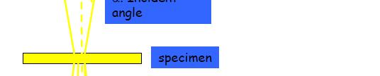
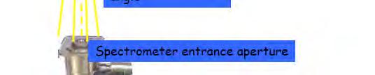
6 What else? Incident beam specimen Diffracted electrons 2Θ Transmitted electrons Energy loss electrons EELS
 intensity jumps ionization energy levels => edges =core level distributions")

 Inelastic")
 = ε 2 unoccupied DOS Energy Loss Near Edge fine")
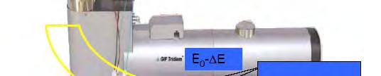
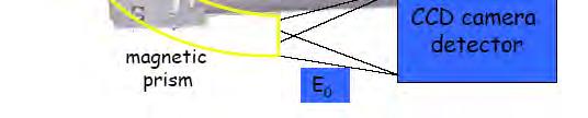
7 Electron Energy Loss Spectroscopy E V E F M L K BC BV Im(-1/ε) = ε 2 / (ε 1 2 +ε 2 2 ) intensity jumps ionization energy levels => edges =core level distributions Low-losses (the first few ten ev) Valence electrons (VEELS) Collective excitation : Plasmon Individual excitation :Interband Transition Thickness: I t /I zl =t/λ p Dielectric function ε = ε 1 + i ε 2 Optical parameters n, k, μ, R = f (ε 1, ε 2 ) Electronic structure ε 2 JDOS Core-losses (up to a few thousand ev) Inelastic interactions with inner or core level electrons Elemental l quantitative analysis Electronic structure I~Im(-1/ε) = ε 2 unoccupied DOS Energy Loss Near Edge fine Structure ELNES


8 Electron Energy Loss Spectroscopy
9 Electron Energy Loss Spectroscopy. Electron Energy Loss Spectroscopy Energy filtered TEM
10 TEM/EELS EELS adds one dimension to TEM imaging By probing the excitations ti of electrons bounded dto the solid with the electrons from the incident beam Gives information on: specimen thickness elemental chemical composition and spatial distribution of elements spatial distribution of first neighbors relative to an atomic site chemical bonding electronic band structure dielectric function with an energy resolution ranging between 1 ev and 0.3 ev with a spatial resolution ranging between 10 nm and 1 nm
11 Concept of holography Complex wave : amplitude and phase Take a picture : Ψ = Ae iϕ I = Ψ ² = A² You loose the phase ϕ!!! We want to retrieve the phase! Object Coherent photon wave Object wave Reference wave I = Ψ ref + Ψ object ² = Aref ² + Aobject² + 2Aref Aobject cos(2π R0 x + ϕobject ϕref )

 dz E φ M e x)")

12 Information in the phase E φ ( x) = C V ( x, z ) dz E φ M e x) = - B (x,z) dxdz h ( n T M φ = φ + φ E

) Objective lens")

 + 2As(x,y)cos[ 2πR")
13 Electron Holography in a TEM Sample ψ o= exp( ik.r) ψ s= As ( r)exp( i K.r+ ϕs( r)) Objective lens Focal plane V+ Image plane Projector lenses I = Ψ Ψ s* 2 2 Holo o =1+A +As (x,y ) + 2As(x,y)cos[ 2πR 0.x+ ϕs(x,y)]


14 GPA analysis of the hologram FT Mask FT 1 π < ϕ < π Image d amplitude A s (x, y) 2π jumps unwrapped Image de phase ϕ s (x,y)


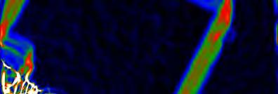
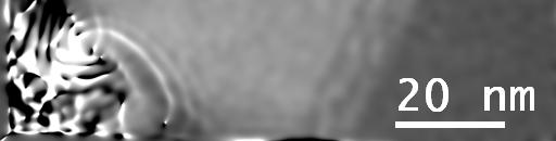
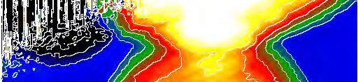
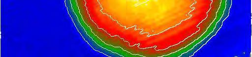
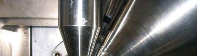
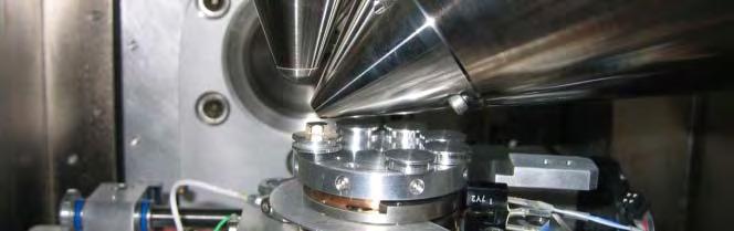
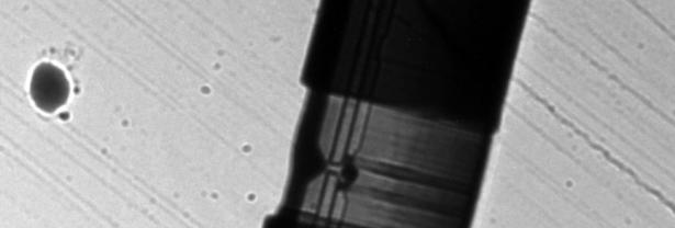
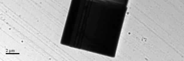
15 Experimental aspects Coherent Electron Beam Field Emission Gun Fresnel fringes due to the high h coherence of the beam Elliptic illumination to increase the spatial coherence biprism meilleure cohérence


 20")


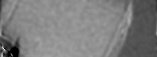
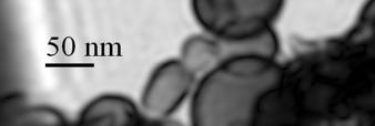
16 Hologram with the object Reference hologram (without object) FT FT 20 nm FT -1 FT -1 Ιs = A i s e ϕs Ι R = A R e iϕ R Ιs Ι R = A s A R e i( ϕs ϕ R ) 20 nm Dérivée de la phase Normalised Amplitude A s A R = A N Phase shift due to the object only ϕs ϕ R = Δϕ
17 Non magnetic sample (B = 0) e ϕ(xϕ ( x, y) = C V ( x, y, z ) dz Bn ( x, y, z ) dxdz E h ϕelect ( x, y) = C V ( x, y, z)d dz E with : C E = 2π λ E + E 0 E(E + 2E 0 ) V(x,y,z) = V i (x,y,z) + V (x,y,z) V i (x,y,z) = Mean Inner Potential (MIP) V (x,y,z) = Local electric potential (junctions, CMOS, diode..) if V i et V are constants along the e-beam direction «z» : ϕ elect = C E (V i + V ) t t = sample thickness Need to perfectly know the sample thickness (sphere, cleaved sample, CBED thickness measurement...) to quantify V i and V


18 Mean Inner Potential (MIP) measurement ϕ elect = C E V i t Fe 0.5 Ni nm 10 nm


19 Fe 0.3 Ni nm Phase/radians s FeNi theory FeNi exp c 0 φ = c V t E Position/nm MIP measurement Composition analysis Morphological studies
20 Magnetic samples ϕ( x) = C e E V(x,z)dz Bn(x,z) dxdz h Pb. 1: The objective must be witched off. => use of Lorentz lens to get sufficient resolution Object in a magnetic field free area Field of view up to 1µm f = 30 mm Cs = 7430 mm (!!) Cc = 39 mm Point resolution # 2 nm


 dd dxdz h Total phase")
21 Magnetic samples Pb. 2: How to separate the magnetic and electrostatic contributions B and C E V i t? Phase shift induced bt the local electrostatic potential: ϕ elect ( x) E ) = C V ( x, z dz Phase shift induced by the local magnetic field : ϕ mag e ( x) = - Bn (x,z) dd dxdz h Total phase shift ϕ ( x) = ϕ (x) + ϕ (x) Tot ( elect mag
22 Pb. 2: How to separate the magnetic and electrostatic contributions B and C E V i t? 1/ Taking two holograms (4 with the reference holograms) switching upside down the sample => The sign of the magnetic contribution is reversed and the electrostatic one remains. t V i B V i B e ϕ 1 = C E V i. t B n ds e h ϕ 2 C. t + ϕ -ϕ 2 1 h e = 2 B ds n ϕ +ϕ = 2 1 = E V i B n ds h 2C E V t Problem : finding back the same area of interest 2/ Taking two holograms with two different high voltages 2π E + E0 CE = λ E(E + 2E 0 ) e ϕ 1 = C E V i. t B n ds ϕ -ϕ h V i t = e ( CE C E ) ϕ 2 = C E V i. t B n ds h Problem : keeping the same acquisition iiti conditions (magnification, alignment ) when changing the high voltage. i
23 3/ Using the high magnetic field of the objective (~2 Tesla) to saturate the magnetic sample in two opposite directions H Objective H Objective H Objective +Θ -Θ Back to Θ = 0 objective switch off t ϕ 1 = C E V.t e i.t. h B n (x). dx ϕ 2 = C E V.t+ e i.t. h B n (x). dx e ϕ - 2 ϕ ϕ + ϕ.t. B n (x).dx = 1 C E V i t = h ϕ 1 Magnetic contribution to the Electrostatic contribution to the phase shift phase shift
.")

24 x 1 = = = Δ dz d z y B e y x y x n x ξ ξ ϕ ϕ ϕ ξ ),, ( ), ( ), ( h t x B e x x n ). ( ) ( h = ϕ The gradient of the phase is proportional to the in plane component of the magnetic induction B n The equiphase contour gives the direction of the magnetic induction B


 TEM")


25 Magnetic Configuration of an isolated Fe Nanocube al., Nano Lett Snoeck et a ), pp t., 2008, 8 (12 (a) TEM image, (b) Magnetic contribution to the phase shift, (c) Magnetic induction mapping, (d) micromagnetic simulation (OOMMF)
26 Magnetic Configuration of two neighbouring Fe Nanocubes (a) TEM image, (b) Magnetic contribution to the phase shift, (c) Magnetic induction () g,( ) g p, () g mapping, (d) micromagnetic simulation (OOMMF)


")


27 Magnetic Configuration of four neighbouring Fe Nanocubes (a) TEM image, (b) Magnetic contribution to the phase shift, (c) Magnetic induction mapping, (d) micromagnetic simulation (OOMMF)
")
/dx = (e")


28 Magnetic multilayers φ(x) = e/ħ B (x) t(x) dx dφ(x)/dx = (e / ħ). t. B (x) E. Snoeck, P. Baules, G. BenAssayag, C. Tiusan, F. Greullet, M. Hehn, A. Schuhl J. Phys.: Condens. Matter 20 (2008)
29 Sample preparation Cross Section glue specimen 1t 1st cut specimen Ar+ ions electrons 2nd cut Mechanical grinding (abrasive papers + dimpler) > µm + ion milling > hole Ready for TEM
30 Sample preparation Plan view Ar+ ions electrons 20 µm specimen mechanical grinding + dimpling ion milling > hole Ready for TEM
31 Sample preparation Sample preparation
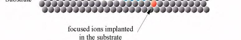
32 Sample preparation: FIB
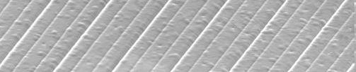
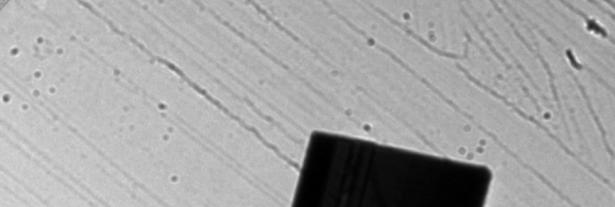
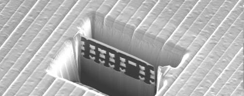
33 Sample preparation: FIB
34 Summary Good TEM results from 50% specimen preparation, 20% TEM s price 30% guy s experience
Transmission Electron Microscopy
 L. Reimer H. Kohl Transmission Electron Microscopy Physics of Image Formation Fifth Edition el Springer Contents 1 Introduction... 1 1.1 Transmission Electron Microscopy... 1 1.1.1 Conventional Transmission
CHEM 681 Seminar Mingqi Zhao April 20, 1998 Room 2104, 4:00 p.m. High Resolution Transmission Electron Microscopy: theories and applications
 CHEM 681 Seminar Mingqi Zhao April 20, 1998 Room 2104, 4:00 p.m. High Resolution Transmission Electron Microscopy: theories and applications In materials science, people are always interested in viewing
High-Resolution. Transmission. Electron Microscopy
 Part 4 High-Resolution Transmission Electron Microscopy 186 Significance high-resolution transmission electron microscopy (HRTEM): resolve object details smaller than 1nm (10 9 m) image the interior of
Supplementary Note 1 Description of the sample and thin lamella preparation Supplementary Figure 1 FeRh lamella prepared by FIB and used for in situ
 Supplementary Note 1 Description of the sample and thin lamella preparation A 5nm FeRh layer was epitaxially grown on a go (1) substrate by DC sputtering using a co-deposition process from two pure Fe
Spatial Frequency and Transfer Function. columns of atoms, where the electrostatic potential is higher than in vacuum
 Image Formation Spatial Frequency and Transfer Function consider thin TEM specimen columns of atoms, where the electrostatic potential is higher than in vacuum electrons accelerate when entering the specimen
ELECTRON HOLOGRAPHY OF NANOSTRUCTURED MAGNETIC MATERIALS. Now at: Department of Materials, University of Oxford, Parks Road, Oxford OX1 3PH, UK
 ELECTRON HOLOGRAPHY OF NANOSTRUCTURED MAGNETIC MATERIALS R. E. DUNIN-BORKOWSKI a,b, B. KARDYNAL c,d, M. R. MCCARTNEY a, M. R. SCHEINFEIN e,f, DAVID J. SMITH a,e a Center for Solid State Science, Arizona
Overview of scattering, diffraction & imaging in the TEM
 Overview of scattering, diffraction & imaging in the TEM Eric A. Stach Purdue University Scattering Electrons, photons, neutrons Radiation Elastic Mean Free Path (Å)( Absorption Length (Å)( Minimum Probe
Lecture 20 Optical Characterization 2
 Lecture 20 Optical Characterization 2 Schroder: Chapters 2, 7, 10 1/68 Announcements Homework 5/6: Is online now. Due Wednesday May 30th at 10:00am. I will return it the following Wednesday (6 th June).
Aberration-corrected TEM studies on interface of multilayered-perovskite systems
 Aberration-corrected TEM studies on interface of multilayered-perovskite systems By Lina Gunawan (0326114) Supervisor: Dr. Gianluigi Botton November 1, 2006 MSE 702(1) Presentation Outline Literature Review
MSE 321 Structural Characterization
 Auger Spectroscopy Auger Electron Spectroscopy (AES) Scanning Auger Microscopy (SAM) Incident Electron Ejected Electron Auger Electron Initial State Intermediate State Final State Physical Electronics
April 10th-12th, 2017
 Thomas LaGrange, Ph.D. Faculty Lecturer and Senior Staff Scientist Introduction: Basics of Transmission Electron Microscopy (TEM) TEM Doctoral Course MS-637 April 10th-12th, 2017 Outline 1. What is microcopy?
Electron microscopy in molecular cell biology I
 Electron microscopy in molecular cell biology I Electron optics and image formation Werner Kühlbrandt Max Planck Institute of Biophysics chemistry biology Objects of interest Galaxy 10 6 light years 10
Dislocation networks in graphite
 Dislocation networks in graphite High Resolution Microscop With Reference to Lattice Fringe Imaging in a TEM f f r Real space Specimen Reciprocal space hr Point spread function Diffraction pattern Back
= 6 (1/ nm) So what is probability of finding electron tunneled into a barrier 3 ev high?
 So what is probability of finding electron tunneled into a barrier 3 ev high?") STM STM With a scanning tunneling microscope, images of surfaces with atomic resolution can be readily obtained. An STM uses quantum tunneling of electrons to map the density of electrons on the surface
STM STM With a scanning tunneling microscope, images of surfaces with atomic resolution can be readily obtained. An STM uses quantum tunneling of electrons to map the density of electrons on the surface
Elastic and Inelastic Scattering in Electron Diffraction and Imaging
 Elastic and Inelastic Scattering in Electron Diffraction and Imaging Contents Introduction Symbols and definitions Part A Diffraction and imaging of elastically scattered electrons Chapter 1. Basic kinematical
Lecture 5. X-ray Photoemission Spectroscopy (XPS)
") Lecture 5 X-ray Photoemission Spectroscopy (XPS) 5. Photoemission Spectroscopy (XPS) 5. Principles 5.2 Interpretation 5.3 Instrumentation 5.4 XPS vs UV Photoelectron Spectroscopy (UPS) 5.5 Auger Electron
Lecture 5 X-ray Photoemission Spectroscopy (XPS) 5. Photoemission Spectroscopy (XPS) 5. Principles 5.2 Interpretation 5.3 Instrumentation 5.4 XPS vs UV Photoelectron Spectroscopy (UPS) 5.5 Auger Electron
Homework 1. Nano Optics, Fall Semester 2018 Photonics Laboratory, ETH Zürich
 Homework 1 Contact: mfrimmer@ethz.ch Due date: Friday 12 October 2018; 10:00 a.m. Nano Optics, Fall Semester 2018 Photonics Laboratory, ETH Zürich www.photonics.ethz.ch The goal of this homework is to
Structure analysis: Electron diffraction LEED TEM RHEED
 Structure analysis: Electron diffraction LEED: Low Energy Electron Diffraction SPA-LEED: Spot Profile Analysis Low Energy Electron diffraction RHEED: Reflection High Energy Electron Diffraction TEM: Transmission
Energy-Filtering. Transmission. Electron Microscopy
 Part 3 Energy-Filtering Transmission Electron Microscopy 92 Energy-Filtering TEM Principle of EFTEM expose specimen to mono-energetic electron radiation inelastic scattering in the specimen poly-energetic
CHEM-E5225 :Electron Microscopy Imaging
 CHEM-E5225 :Electron Microscopy Imaging 2016.10 Yanling Ge Outline Planar Defects Image strain field WBDF microscopy HRTEM information theory Discuss of question homework? Planar Defects - Internal Interface
Core-Level spectroscopy. Experiments and first-principles calculations. Tomoyuki Yamamoto. Waseda University, Japan
 Core-Level spectroscopy Experiments and first-principles calculations Tomoyuki Yamamoto Waseda University, Japan 22 nd WIEN2k workshop Jun. 26 th, 2015@Singapore Outline What is core-level spectroscopy
Experimental methods in Physics. Electron Microscopy. Basic Techniques (MEP-I) SEM, TEM
 SEM, TEM") Experimental methods in Physics Electron Microscopy Basic Techniques (MEP-I) SEM, TEM Advanced Techniques (MEP-II) HR-TEM, STEM Analytical-TEM 3D-Microscopy Spring 2012 Experimental Methods in Physics
Experimental methods in Physics Electron Microscopy Basic Techniques (MEP-I) SEM, TEM Advanced Techniques (MEP-II) HR-TEM, STEM Analytical-TEM 3D-Microscopy Spring 2012 Experimental Methods in Physics
Ecole Franco-Roumaine : Magnétisme des systèmes nanoscopiques et structures hybrides - Brasov, Modern Analytical Microscopic Tools
 1. Introduction Solid Surfaces Analysis Group, Institute of Physics, Chemnitz University of Technology, Germany 2. Limitations of Conventional Optical Microscopy 3. Electron Microscopies Transmission Electron
OPSE FINAL EXAM Fall 2015 YOU MUST SHOW YOUR WORK. ANSWERS THAT ARE NOT JUSTIFIED WILL BE GIVEN ZERO CREDIT.
 CLOSED BOOK. Equation Sheet is provided. YOU MUST SHOW YOUR WORK. ANSWERS THAT ARE NOT JUSTIFIED WILL BE GIVEN ZERO CREDIT. ALL NUMERICAL ANSERS MUST HAVE UNITS INDICATED. (Except dimensionless units like
IMAGING DIFFRACTION SPECTROSCOPY
 TEM Techniques TEM/STEM IMAGING DIFFRACTION SPECTROSCOPY Amplitude contrast (diffracion contrast) Phase contrast (highresolution imaging) Selected area diffraction Energy dispersive X-ray spectroscopy
Probing Matter: Diffraction, Spectroscopy and Photoemission
 Probing Matter: Diffraction, Spectroscopy and Photoemission Anders Nilsson Stanford Synchrotron Radiation Laboratory Why X-rays? VUV? What can we hope to learn? 1 Photon Interaction Incident photon interacts
Transmission Electron Microscopy and Diffractometry of Materials
 Brent Fultz James Howe Transmission Electron Microscopy and Diffractometry of Materials Fourth Edition ~Springer 1 1 Diffraction and the X-Ray Powder Diffractometer 1 1.1 Diffraction... 1 1.1.1 Introduction
h which looks like the classical version, because we used a modified kinetic energy
 1 0. Phase Contrast More on phase contrast The wave number of a high-energy electron in the vacuum can be written menr k h which looks like the classical version, because we used a modified kinetic energy
GRATING CLASSIFICATION
 GRATING CLASSIFICATION SURFACE-RELIEF GRATING TYPES GRATING CLASSIFICATION Transmission or Reflection Classification based on Regime DIFFRACTION BY GRATINGS Acousto-Optics Diffractive Optics Integrated
Electron Microscopy I
 Characterization of Catalysts and Surfaces Characterization Techniques in Heterogeneous Catalysis Electron Microscopy I Introduction Properties of electrons Electron-matter interactions and their applications
Determination of mean inner potential of germanium using off-axis electron holography
 652 Acta Cryst. (1999). A55, 652±658 Determination of mean inner potential of germanium using off-axis electron holography Jing Li, a * M. R. McCartney, b R. E. Dunin-Borkowski b and David J. Smith a a
Chapter 9. Electron mean free path Microscopy principles of SEM, TEM, LEEM
 Chapter 9 Electron mean free path Microscopy principles of SEM, TEM, LEEM 9.1 Electron Mean Free Path 9. Scanning Electron Microscopy (SEM) -SEM design; Secondary electron imaging; Backscattered electron
National Laboratory. 1. Introduction
 Contents electron optics instrumentation Volume 36E Number 1 July 10, 2001 Performance and Capabilities of JEM-3000F to Advanced Materials Characterization at Brookhaven National Laboratory.............
Nature of Light Part 2
 Nature of Light Part 2 Fresnel Coefficients From Helmholts equation see imaging conditions for Single lens 4F system Diffraction ranges Rayleigh Range Diffraction limited resolution Interference Newton
Gaetano L Episcopo. Scanning Electron Microscopy Focus Ion Beam and. Pulsed Plasma Deposition
 Gaetano L Episcopo Scanning Electron Microscopy Focus Ion Beam and Pulsed Plasma Deposition Hystorical background Scientific discoveries 1897: J. Thomson discovers the electron. 1924: L. de Broglie propose
Methods of surface analysis
 Methods of surface analysis Nanomaterials characterisation I RNDr. Věra Vodičková, PhD. Surface of solid matter: last monoatomic layer + absorbed monolayer physical properties are effected (crystal lattice
KMÜ 396 MATERIALS SCIENCE AND TECH. I PRESENTATION ELECTRON ENERGY LOSS SPECTROSCOPY (EELS) TUĞÇE SEZGİN
 TUĞÇE SEZGİN") KMÜ 396 MATERIALS SCIENCE AND TECH. I PRESENTATION ELECTRON ENERGY LOSS SPECTROSCOPY (EELS) TUĞÇE SEZGİN 20970725 HACETTEPE UNIVERSITY DEPARTMENT OF CHEMICAL ENGINEERING, SPRING 2011,APRIL,ANKARA CONTENTS
KMÜ 396 MATERIALS SCIENCE AND TECH. I PRESENTATION ELECTRON ENERGY LOSS SPECTROSCOPY (EELS) TUĞÇE SEZGİN 20970725 HACETTEPE UNIVERSITY DEPARTMENT OF CHEMICAL ENGINEERING, SPRING 2011,APRIL,ANKARA CONTENTS
Interaction X-rays - Matter
 Interaction X-rays - Matter Pair production hν > M ev Photoelectric absorption hν MATTER hν Transmission X-rays hν' < hν Scattering hν Decay processes hν f Compton Thomson Fluorescence Auger electrons
Chapter 4 Imaging Lecture 24
 Chapter 4 Imaging Lecture 4 d (110) Final Exam Notice Time and Date: :30 4:30 PM, Wednesday, Dec. 10, 08. Place: Classroom CHEM-10 Coverage: All contents after midterm Open note Term project is due today
EE 527 MICROFABRICATION. Lecture 5 Tai-Chang Chen University of Washington
 EE 527 MICROFABRICATION Lecture 5 Tai-Chang Chen University of Washington MICROSCOPY AND VISUALIZATION Electron microscope, transmission electron microscope Resolution: atomic imaging Use: lattice spacing.
MS482 Materials Characterization ( 재료분석 ) Lecture Note 4: XRF
 Lecture Note 4: XRF") 2016 Fall Semester MS482 Materials Characterization ( 재료분석 ) Lecture Note 4: XRF Byungha Shin Dept. of MSE, KAIST 1 Course Information Syllabus 1. Overview of various characterization techniques (1 lecture)
2016 Fall Semester MS482 Materials Characterization ( 재료분석 ) Lecture Note 4: XRF Byungha Shin Dept. of MSE, KAIST 1 Course Information Syllabus 1. Overview of various characterization techniques (1 lecture)
Homework 1. Nano Optics, Fall Semester 2017 Photonics Laboratory, ETH Zürich
 Homework 1 Contact: mfrimmer@ethz.ch Due date: Friday 13.10.2017; 10:00 a.m. Nano Optics, Fall Semester 2017 Photonics Laboratory, ETH Zürich www.photonics.ethz.ch The goal of this homework is to establish
November 30th -December 2 nd, st 2nd 3rd. 8:15 7)HRTEM 10) TEM imaging and diffraction examples. 9:15 8)HRTEM 10) Diffraction going further
HRTEM 10) TEM imaging and diffraction examples. 9:15 8)HRTEM 10) Diffraction going further") Thomas LaGrange, Ph.D. Faculty and Staff Scientist Introduction: Basics of Transmission Electron Microscopy (TEM) TEM Doctoral Course MS-637 November 30th -December 2 nd, 2015 Planning MSE-637 TEM -basics
Thomas LaGrange, Ph.D. Faculty and Staff Scientist Introduction: Basics of Transmission Electron Microscopy (TEM) TEM Doctoral Course MS-637 November 30th -December 2 nd, 2015 Planning MSE-637 TEM -basics
Light matter interaction. Ground state spherical electron cloud. Excited state : 4 quantum numbers n principal (energy)
") Light matter interaction Hydrogen atom Ground state spherical electron cloud Excited state : 4 quantum numbers n principal (energy) L angular momentum, 2,3... L L z projection of angular momentum S z projection
Light matter interaction Hydrogen atom Ground state spherical electron cloud Excited state : 4 quantum numbers n principal (energy) L angular momentum, 2,3... L L z projection of angular momentum S z projection
Conventional Transmission Electron Microscopy. Introduction. Text Books. Text Books. EMSE-509 CWRU Frank Ernst
 Text Books Conventional Transmission Electron Microscopy EMSE-509 CWRU Frank Ernst D. B. Williams and C. B. Carter: Transmission Electron Microscopy, New York: Plenum Press (1996). L. Reimer: Transmission
Photon Interaction. Spectroscopy
 Photon Interaction Incident photon interacts with electrons Core and Valence Cross Sections Photon is Adsorbed Elastic Scattered Inelastic Scattered Electron is Emitted Excitated Dexcitated Stöhr, NEXAPS
Lecture 3. Profiling the electrostatic field and charge distributions using electron holography. F. A. Ponce, J. Cai and M.
 Lecture 3 Profiling the electrostatic field and charge distributions using electron holography F. A. Ponce, J. Cai and M. Stevens Department of Physics and Astronomy Arizona State University Tempe, Arizona,
ME equations. Cylindrical symmetry. Bessel functions 1 kind Bessel functions 2 kind Modifies Bessel functions 1 kind Modifies Bessel functions 2 kind
 Δϕ=0 ME equations ( 2 ) Δ + k E = 0 Quasi static approximation Dynamic approximation Cylindrical symmetry Metallic nano wires Nano holes in metals Bessel functions 1 kind Bessel functions 2 kind Modifies
Transmission Electron Microscope. Experimental Instruction
 Transmission Electron Microscope Experimental Instruction In advanced practical course [F-Praktikum] Date: April 2017 Contents 1 Task 3 2 Theoretical Basics 3 2.1 Bragg Diffraction......................................
QUANTUM PHYSICS. Limitation: This law holds well only for the short wavelength and not for the longer wavelength. Raleigh Jean s Law:
 Black body: A perfect black body is one which absorbs all the radiation of heat falling on it and emits all the radiation when heated in an isothermal enclosure. The heat radiation emitted by the black
Direct study of domain and domain wall structure in magnetic films and nanostructures
 Direct study of domain and domain wall structure in magnetic films and nanostructures John Chapman, University of Glasgow Synopsis Why use Lorentz microscopy? Magnetisation reversal in soft magnetic films
Energy-Filtered High-Resolution Electron Microscopy for Quantitative Solid State Structure Determination
 [J. Res. Natl. Inst. Stand. Technol. 102, 1 (1997)] Energy-Filtered High-Resolution Electron Microscopy for Quantitative Solid State Structure Determination Volume 102 Number 1 January February 1997 Z.
Characterization of the magnetic properties of a GdBa 2 Cu 3 O 7 /La 0.75 Sr 0.25 MnO 3 superlattice using off-axis electron holography
 Applied Surface Science 252 (2006) 3977 3983 www.elsevier.com/locate/apsusc Characterization of the magnetic properties of a GdBa 2 Cu 3 O 7 /La 0.75 Sr 0.25 MnO 3 superlattice using off-axis electron
MSE 321 Structural Characterization
 Auger Spectroscopy Auger Electron Spectroscopy (AES) Scanning Auger Microscopy (SAM) Incident Electron Ejected Electron Auger Electron Initial State Intermediate State Final State Physical Electronics
object objective lens eyepiece lens
 Advancing Physics G495 June 2015 SET #1 ANSWERS Field and Particle Pictures Seeing with electrons The compound optical microscope Q1. Before attempting this question it may be helpful to review ray diagram
MT Electron microscopy Scanning electron microscopy and electron probe microanalysis
 MT-0.6026 Electron microscopy Scanning electron microscopy and electron probe microanalysis Eero Haimi Research Manager Outline 1. Introduction Basics of scanning electron microscopy (SEM) and electron
Transmission Electron Microscopy. Part #1 Diffraction Conventional Imaging
 Transmission Electron Microscopy Part #1 Diffraction Conventional Imaging Nicolas Menguy Institut de Minéralogie, de Physique des Matériaux et de Cosmochimie Outline Part 1 : Conventional TEM - Transmission
Light Propagation in Free Space
 Intro Light Propagation in Free Space Helmholtz Equation 1-D Propagation Plane waves Plane wave propagation Light Propagation in Free Space 3-D Propagation Spherical Waves Huygen s Principle Each point
Interactions with Matter
 Manetic Lenses Manetic fields can displace electrons Manetic field can be produced by passin an electrical current throuh coils of wire Manetic field strenth can be increased by usin a soft ferromanetic
PHY410 Optics Exam #3
 PHY410 Optics Exam #3 NAME: 1 2 Multiple Choice Section - 5 pts each 1. A continuous He-Ne laser beam (632.8 nm) is chopped, using a spinning aperture, into 500 nanosecond pulses. Compute the resultant
Electron and electromagnetic radiation
 Electron and electromagnetic radiation Generation and interactions with matter Stimuli Interaction with sample Response Stimuli Waves and energy The energy is propotional to 1/λ and 1/λ 2 λ λ 1 Electromagnetic
X-Ray Spectro-Microscopy Joachim Stöhr Stanford Synchrotron Radiation Laboratory
 X-Ray Spectro-Microscopy Joachim Stöhr Stanford Synchrotron Radiation Laboratory X-Rays have come a long way Application to Magnetic Systems 1 µm 1895 1993 2003 http://www-ssrl.slac.stanford.edu/stohr/index.htm
Controlled double-slit electron diffraction
 1 Controlled double-slit electron diffraction Roger Bach 1, Damian Pope 2, Sy-Hwang Liou 1 and Herman Batelaan 1 1 Department of Physics and Astronomy, University of Nebraska-Lincoln, Theodore P. Jorgensen
Chemical Analysis in TEM: XEDS, EELS and EFTEM. HRTEM PhD course Lecture 5
 Chemical Analysis in TEM: XEDS, EELS and EFTEM HRTEM PhD course Lecture 5 1 Part IV Subject Chapter Prio x-ray spectrometry 32 1 Spectra and mapping 33 2 Qualitative XEDS 34 1 Quantitative XEDS 35.1-35.4
Quarterly. Electron Holography and Rock Magnetism. The IRM. Inside...
 Quarterly The IRM Winter 2007, Vol. 16 No. 4 Inside... page 2 Visiting Fellows Reports page 10 Current Articles Electron Holography and Rock Magnetism Joshua Feinberg 1,2 Richard Harrison 1 Takeshi Kasama
EE485 Introduction to Photonics
 Pattern formed by fluorescence of quantum dots EE485 Introduction to Photonics Photon and Laser Basics 1. Photon properties 2. Laser basics 3. Characteristics of laser beams Reading: Pedrotti 3, Sec. 1.2,
The Electromagnetic Properties of Materials
 The Electromagnetic Properties of Materials Electrical conduction Metals Semiconductors Insulators (dielectrics) Superconductors Magnetic materials Ferromagnetic materials Others Photonic Materials (optical)
THE UNIVERSITY OF NEW SOUTH WALES SCHOOL OF PHYSICS FINAL EXAMINATION JUNE/JULY PHYS3080 Solid State Physics
 THE UNIVERSITY OF NEW SOUTH WALES SCHOOL OF PHYSICS FINAL EXAMINATION JUNE/JULY 006 PHYS3080 Solid State Physics Time Allowed hours Total number of questions - 5 Answer ALL questions All questions are
Analytical Methods for Materials
 Analytical Methods for Materials Lesson 21 Electron Microscopy and X-ray Spectroscopy Suggested Reading Leng, Chapter 3, pp. 83-126; Chapter 4, pp. 127-160; Chapter 6, pp. 191-219 P.J. Goodhew, J. Humphreys
Linear Systems. : object : image. Describes the output of a linear system. input. output. Impulse response function
 Linear Systems Describes the output of a linear system Gx FxHx- xdx FxHx F x G x x output input Impulse response function H x xhx- xdx x If the microscope is a linear system: : object : image G x S F x
Electron Holography of Ferromagnetic Nanoparticles Encapsulated in Three-Dimensional Arrays of Aligned Carbon Nanotubes
 Mater. Res. Soc. Symp. Proc. Vol. 962 2007 Materials Research Society 0962-P13-03 Electron Holography of Ferromagnetic Nanoparticles Encapsulated in Three-Dimensional Arrays of Aligned Carbon Nanotubes
CHARACTERIZATION of NANOMATERIALS KHP
 CHARACTERIZATION of NANOMATERIALS Overview of the most common nanocharacterization techniques MAIN CHARACTERIZATION TECHNIQUES: 1.Transmission Electron Microscope (TEM) 2. Scanning Electron Microscope
sin" =1.22 # D "l =1.22 f# D I: In introduction to molecular electron microscopy - Imaging macromolecular assemblies
 I: In introduction to molecular electron microscopy - Imaging macromolecular assemblies Yifan Cheng Department of Biochemistry & Biophysics office: GH-S472D; email: ycheng@ucsf.edu 2/20/2015 - Introduction
Electron Biprism in the Condenser System for CHIRALTEM Experiment
 Fakultät Mathematik und Naturwissenschaften, Institut für Strukturphysik Electron Biprism in the Condenser System for CHIRALTEM Experiment Petr Formánek, Bernd Einenkel, Hannes Lichte Speziallabor Triebenberg
Lecture 19 Optical MEMS (1)
") EEL6935 Advanced MEMS (Spring 5) Instructor: Dr. Huikai Xie Lecture 19 Optical MEMS (1) Agenda: Optics Review EEL6935 Advanced MEMS 5 H. Xie 3/8/5 1 Optics Review Nature of Light Reflection and Refraction
EEL6935 Advanced MEMS (Spring 5) Instructor: Dr. Huikai Xie Lecture 19 Optical MEMS (1) Agenda: Optics Review EEL6935 Advanced MEMS 5 H. Xie 3/8/5 1 Optics Review Nature of Light Reflection and Refraction
Film Characterization Tutorial G.J. Mankey, 01/23/04. Center for Materials for Information Technology an NSF Materials Science and Engineering Center
 Film Characterization Tutorial G.J. Mankey, 01/23/04 Theory vs. Experiment A theory is something nobody believes, except the person who made it. An experiment is something everybody believes, except the
Spectroscopies for Unoccupied States = Electrons
 Spectroscopies for Unoccupied States = Electrons Photoemission 1 Hole Inverse Photoemission 1 Electron Tunneling Spectroscopy 1 Electron/Hole Emission 1 Hole Absorption Will be discussed with core levels
Phys 531 Lecture 27 6 December 2005
 Phys 531 Lecture 27 6 December 2005 Final Review Last time: introduction to quantum field theory Like QM, but field is quantum variable rather than x, p for particle Understand photons, noise, weird quantum
Physical Principles of Electron Microscopy. 2. Electron Optics
 Physical Principles of Electron Microscopy 2. Electron Optics Ray Egerton University of Alberta and National Institute of Nanotechnology Edmonton, Canada www.tem-eels.ca regerton@ualberta.ca Properties
Optical Properties of Solid from DFT
 Optical Properties of Solid from DFT 1 Prof.P. Ravindran, Department of Physics, Central University of Tamil Nadu, India & Center for Materials Science and Nanotechnology, University of Oslo, Norway http://folk.uio.no/ravi/cmt15
STM spectroscopy (STS)
") STM spectroscopy (STS) di dv 4 e ( E ev, r) ( E ) M S F T F Basic concepts of STS. With the feedback circuit open the variation of the tunneling current due to the application of a small oscillating voltage
STM spectroscopy (STS) di dv 4 e ( E ev, r) ( E ) M S F T F Basic concepts of STS. With the feedback circuit open the variation of the tunneling current due to the application of a small oscillating voltage
Physics 214 Midterm Exam Spring Last Name: First Name NetID Discussion Section: Discussion TA Name:
 Physics 214 Midterm Exam Spring 215 Last Name: First Name NetID Discussion Section: Discussion TA Name: Instructions Turn off your cell phone and put it away. Keep your calculator on your own desk. Calculators
Introduction to X-ray Photoelectron Spectroscopy (XPS) XPS which makes use of the photoelectric effect, was developed in the mid-1960
 XPS which makes use of the photoelectric effect, was developed in the mid-1960") Introduction to X-ray Photoelectron Spectroscopy (XPS) X-ray Photoelectron Spectroscopy (XPS), also known as Electron Spectroscopy for Chemical Analysis (ESCA) is a widely used technique to investigate
Introduction to X-ray Photoelectron Spectroscopy (XPS) X-ray Photoelectron Spectroscopy (XPS), also known as Electron Spectroscopy for Chemical Analysis (ESCA) is a widely used technique to investigate
Lecture 5: Characterization methods
 Lecture 5: Characterization methods X-Ray techniques Single crystal X-Ray Diffration (XRD) Powder XRD Thin film X-Ray Reflection (XRR) Microscopic methods Optical microscopy Electron microscopies (SEM,
Lecture notes 5: Diffraction
 Lecture notes 5: Diffraction Let us now consider how light reacts to being confined to a given aperture. The resolution of an aperture is restricted due to the wave nature of light: as light passes through
Chapter 10. Interference of Light
 Chapter 10. Interference of Light Last Lecture Wave equations Maxwell equations and EM waves Superposition of waves This Lecture Two-Beam Interference Young s Double Slit Experiment Virtual Sources Newton
1. Consider the biconvex thick lens shown in the figure below, made from transparent material with index n and thickness L.
 Optical Science and Engineering 2013 Advanced Optics Exam Answer all questions. Begin each question on a new blank page. Put your banner ID at the top of each page. Please staple all pages for each individual
Techniques EDX, EELS et HAADF en TEM: possibilités d analyse et applications
 Techniques EDX, EELS et HAADF en TEM: possibilités d analyse et applications Thomas Neisius Université Paul Cézanne Plan Imaging modes HAADF Example: supported Pt nanoparticles Electron sample interaction
DIFFRACTION PHYSICS THIRD REVISED EDITION JOHN M. COWLEY. Regents' Professor enzeritus Arizona State University
 DIFFRACTION PHYSICS THIRD REVISED EDITION JOHN M. COWLEY Regents' Professor enzeritus Arizona State University 1995 ELSEVIER Amsterdam Lausanne New York Oxford Shannon Tokyo CONTENTS Preface to the first
AP5301/ Name the major parts of an optical microscope and state their functions.
 Review Problems on Optical Microscopy AP5301/8301-2015 1. Name the major parts of an optical microscope and state their functions. 2. Compare the focal lengths of two glass converging lenses, one with
Table of Content. Mechanical Removing Techniques. Ultrasonic Machining (USM) Sputtering and Focused Ion Beam Milling (FIB)
 Sputtering and Focused Ion Beam Milling (FIB)") Table of Content Mechanical Removing Techniques Ultrasonic Machining (USM) Sputtering and Focused Ion Beam Milling (FIB) Ultrasonic Machining In ultrasonic machining (USM), also called ultrasonic grinding,
Table of Content Mechanical Removing Techniques Ultrasonic Machining (USM) Sputtering and Focused Ion Beam Milling (FIB) Ultrasonic Machining In ultrasonic machining (USM), also called ultrasonic grinding,
Modeling Focused Beam Propagation in scattering media. Janaka Ranasinghesagara, Ph.D.
 Modeling Focused Beam Propagation in scattering media Janaka Ranasinghesagara, Ph.D. Teaching Objectives The need for computational models of focused beam propagation in scattering media Introduction to
MS482 Materials Characterization ( 재료분석 ) Lecture Note 5: RBS
 Lecture Note 5: RBS") 2016 Fall Semester MS482 Materials Characterization ( 재료분석 ) Lecture Note 5: RBS Byungha Shin Dept. of MSE, KAIST 1 Course Information Syllabus 1. Overview of various characterization techniques (1 lecture)
2016 Fall Semester MS482 Materials Characterization ( 재료분석 ) Lecture Note 5: RBS Byungha Shin Dept. of MSE, KAIST 1 Course Information Syllabus 1. Overview of various characterization techniques (1 lecture)
Atomic Diffraction Microscope of the de Broglie Waves
 ISSN 5-66X, Laser Physics,, Vol., No., pp. 7 5. Pleiades Publishing, Ltd.,. Original Russian Text Astro, Ltd.,. PAPERS Atomic Diffraction Microscope of the de Broglie Waves V. I. Balykin Institute of Spectroscopy,
Chapter 16 Holography
 Chapter 16 Holography Virtually all recording devices for light respond to light intensity. Problem: How to record, and then later reconstruct both the amplitude and phase of an optical wave. [This question
Part 3 - Image Formation
 Part 3 - Image Formation Three classes of scattering outcomes Types of electron microscopes Example SEM image: fly nose Example TEM image: muscle Skeletal muscle. Cell and Tissue Ultrastructure Mercer
Everhart-Thornley detector
 SEI Detector Everhart-Thornley detector Microscope chamber wall Faraday cage Scintillator Electrons in Light pipe Photomultiplier Electrical signal out Screen Quartz window +200 V +10 kv Always contains
Secondary Ion Mass Spectroscopy (SIMS)
") Secondary Ion Mass Spectroscopy (SIMS) Analyzing Inorganic Solids * = under special conditions ** = semiconductors only + = limited number of elements or groups Analyzing Organic Solids * = under special
Secondary Ion Mass Spectroscopy (SIMS) Analyzing Inorganic Solids * = under special conditions ** = semiconductors only + = limited number of elements or groups Analyzing Organic Solids * = under special
HOW TO APPROACH SCANNING ELECTRON MICROSCOPY AND ENERGY DISPERSIVE SPECTROSCOPY ANALYSIS. SCSAM Short Course Amir Avishai
 HOW TO APPROACH SCANNING ELECTRON MICROSCOPY AND ENERGY DISPERSIVE SPECTROSCOPY ANALYSIS SCSAM Short Course Amir Avishai RESEARCH QUESTIONS Sea Shell Cast Iron EDS+SE Fe Cr C Objective Ability to ask the
Waves & Oscillations
 Physics 42200 Waves & Oscillations Lecture 32 Electromagnetic Waves Spring 2016 Semester Matthew Jones Electromagnetism Geometric optics overlooks the wave nature of light. Light inconsistent with longitudinal