DESIGN, FABRICATION, AND CHARACTERIZATION OF ELECTROSTATICALLY- ACTUATED SILICON MICRO-MIRRORS
|
|
|
- Meghan Ryan
- 6 years ago
- Views:
Transcription
1 DESIGN, FABRICATION, AND CHARACTERIZATION OF ELECTROSTATICALLY- ACTUATED SILICON MICRO-MIRRORS A Thesis presented to the Faculty of California Polytechnic State University, San Luis Obispo In Partial Fulfillment of the Requirements for the Degree Master of Science in Engineering, with Specialization in Materials Engineering by Dylan Chesbro April 2010
2 2010 Dylan Chesbro ALL RIGHTS RESERVED ii
3 COMMITTEE MEMBERSHIP TITLE: AUTHOR: Design, Fabrication, and Characterization of Electrostaticallyactuated Silicon Torsional Mirrors Dylan Chesbro DATE SUBMITTED: April 2010 COMMITTEE CHAIR: COMMITTEE MEMBER: COMMITTEE MEMBER: Dr. Richard Savage, Professor, Materials Engineering Dr. Blair London, Professor, Materials Engineering Dr. Linda Vanasupa, Professor, Materials Engineering iii
4 ABSTRACT Design, Fabrication, and Characterization of Electrostatically-actuated Silicon Micro Mirrors Dylan Chesbro Micrometer-scale mirrors are used in many electronic devices today such as digital light projection. One common type of mirror is a thin plate structure supported by torsional hinges which rotates when actuated. These devices are popular because the design allows for high stability and reliability. Parallel plate electrostatic actuation is commonly used to create the force which rotates the plate structure. The device consists of one deformable parallel plate electrode and one immovable electrode. In order for these devices to rotate to a specific angle when actuated, both the mechanical and electrostatic forces must be characterized. This project analyzes both of these forces through modeling equations, and compares theoretical performance to experimentally measured values. The rotational measurements involve reflecting a laser spot off the surface of the actuator face and recording any displacement of the laser spot with a position sensitive device. The electrostatic device created consists of a rotating hinged structure, a fixed aluminum electrode, and a polymer spacer to create an air gap between the electrodes. These components are created using standard semiconductor fabrication techniques. The hinged structures are created from a 500μm thick, double-sided polished, single crystal (100) silicon wafer. The wafers are etched using both wet etching, and reactive ion etching techniques, which produce approximately 8μm thick plate structures. Physical vapor deposition is used to deposit a thin aluminum film onto the silicon in order to form a conductive layer. Rigid aluminum counter-electrodes and SU-8 polymer spacers are fabricated on a glass slide. The silicon actuator chip is aligned and mounted onto the glass slide. Once fabricated, the micro-mirror actuator was iv
5 tested for angular rotation as a function of applied voltage. The applied voltage ranged from 0 to 100V and produced an angular rotation up to 0.3 degrees. During testing it was observed that the stability of the angular tilt was poor enough to merit further examination. Angular stability over time can be a serious issue for micro mirrors, and can cause complete failure of the device. Short and long term angular drift as well as a rotational settling phenomenon were investigated. Angular drift was found to be most likely caused by electrical or environmental factors. The rotational settling had an electrical root cause, which caused charge to migrate on the glass substrate beneath the actuator. The charge formed by the migration created a counteracting force on the actuator causing the rotation angle to reduce over time. The migrating charge was eliminated by creating a second neutrally charged counter-electrode which prevented charge from building on the glass surface. Key Words: MEMS, torsional mirror, electrostatic actuation, angular drift, charge migration. v
6 ACKNOWLEGEMENTS It is a pleasure to thank the following people who made this thesis possible: My advisor, Dr. Richard Savage for providing helpful insight into my project, as well as support, and a fully stocked cleanroom. Steve Meredith, Brian Stahl, and Nic Vickers for providing advice and assistance to our microfabrication processing capabilities. The Microsystems Technology Group for maintaining the lab and providing feedback whenever needed. The Cal Poly Materials Engineering Department for providing the resources that made this project possible. vi
7 TABLE OF CONTENTS LIST OF TABLES... VIII LIST OF FIGURES... VIII SECTION 1: INTRODUCTION BACKGROUND MOTIVATION... 2 SECTION 2: OPERATION AND DESIGN DESIRED RESPONSE ELECTROSTATIC ACTUATION Electrostatic and Mechanical Forces Capacitive Charging and Mechanical Response... 9 SECTION 3: TESTING EQUIPMENT MEASUREMENT TEST STAND SECTION 4: DESIGN SUMMARY INITIAL DESIGN EQUATION AND MODELING CONSTRAINTS SECTION 5 FABRICATION SUMMARY THERMAL OXIDATION POSITIVE RESIST PHOTOLITHOGRAPHY AND BOTTOM-SIDE PATTERNING WET ANISOTROPIC ETCHING TOP-SIDE PATTERNING AND DRY ETCHING PHYSICAL VAPOR DEPOSITION COUNTER-ELECTRODE PATTERNING NEGATIVE RESIST PROCESSING FINAL ASSEMBLY FABRICATION ISSUES SECTION 6: POSITIONAL DRIFT OF THE ACTUATOR INTRODUCTION Stability of the Actuator PROCEDURE Long Term Drift Short Term Drift and Rotation Settling RESULTS Long Term Drift Short Term Drift Short Term Rotation Settling DISCUSSION Long and Short Term Drift Short Term Rotation Settling SECTION 7: VOLTAGE VERSUS ROTATION INTRODUCTION vii
8 7.3 RESULTS DISCUSSION SECTION 8: POSITION REPEATABILITY INTRODUCTION PROCEDURE RESULTS DISCUSSION SECTION 9: CONCLUSIONS AND FUTURE WORK REFERENCES LIST OF TABLES Table I - Comparison of Rotation Data Table II - Process Sequence for Wet Thermal Oxide Growth Table III - Positive Photoresist Spin-Coating Program Table IV - Process Specifications for Etching Silicon Using RIE Table V - Process Specifications for Sputtering Al in the Torr Table VI - SU-8 Spin Speed Program LIST OF FIGURES Figure 1 Isometric view (left) of the silicon tortional mirror and side view (right) of the electrostatically actuated device Figure 2 - Model of the torsional hinge silicon plate structure fabricated during this study Figure 3 - The ideal (a) and observed (b) rotational response from an actuator over time Figure 4 - Side view of a micro-mirror actuator displaying the rotation settling phenomenon Figure 5 - Electrostatic actuator which encompasses both mechanical and electrostatic properties Figure 6 - Direct mechanical force from profilometer tip causing actuator rotation Figure 7 - Actuator response to an applied mechanical force showing an average drift of 25nm viii
9 Figure 8 - Overview of the test stand and the system components Figure 9 System block diagram including showing the direction of information Figure 10 - Test stand components which allow for high resolution rotational measurements Figure 11 - Long term drift of used to set a baseline for the test stand measurements Figure 12 - SolidWorks model of the torsional hinge silicon plate structure Figure 13 - FEA model used to predict the rotation angle of the plate structure Figure 14 - Total deflection and length of rotated actuator Figure 15 - Top view of the final silicon actuator design which has a thickness of 8µm Figure 16 - Cross section of a (100) silicon wafer pit demonstrating variable etch rates Figure 17 - Wet silicon etching setup used to create silicon membranes Figure 18 - Depth measurement of an etch pit using the profilometer Figure 19 Cross section of the RIE and actuator showing directionality of etchant Figure 20 - Optical micrograph of the released one axis rotational actuator Figure 21 - Nine patterned aluminum counter-electrodes which are connected to by the bond pad Figure 22 - Assembled actuator chip with six mirrors and external connections Figure 23 - Misalignment of the top and bottom electrodes causes performance issues Figure 24 - Rotational drift of (a) the entire chip and (b) the actuator surface Figure 25 Single long term drift data with a relatively little drift value of seven millidegrees Figure 26 Single long term drift data with a relatively large drift value of 28 millidegrees Figure 27 - Short term drift for a period of 10 minutes at an actuation voltage of 25V Figure 28 - Short term drift for a period of 10 minutes at an actuation voltage of 100V Figure 29 - Comparison of short term drift at six different applied potentials Figure 30 - Initial maximum rotation and subsequent loss over time for an actuation potential of 45V Figure 31 - A compiled graph of five different applied potentials and their similar stabilization times Figure 32 Long term temperature stability of the air showing little fluctuation Figure 33 - Long term rotational drift (left) and the corresponding humidity measurements (right) Figure 34 - Charge migration on the surface of the glass substrate ix
10 Figure 35 - Modified design using a second electrode to eliminate surface charge Figure 36 Elimination of rotation settling when a second electrode is used Figure 37 - Actuator rotation at specific actuating voltages Figure 38 - Compiled graph of actuator rotation comparing the actual rotation to various models Figure 39 Bending of the actuator face causes a larger than predicted force and rotation Figure 40 - Angular repeatability over a period of eight days showing significant drift x
11 SECTION 1: INTRODUCTION 1.1 Background The field of Microelectromechanical systems (MEMS) has seen rapid growth over the past decade with the ability to heavily influence society and the economy [1,2,3]. The fabrication processes used to create MEMS was translated from the integrated circuit manufacturing industry. Translating these processes allowed for high volume production with low unit cost which resulted in the integration of both mechanical and electrical components onto a single chip. In addition to the economic advantages, exclusive applications could be achieved such as micromotors [4], digital-micromirror-devices (DMD) [5], and chemical reactors [6]. It is the scale of these devices that allows for high sensitivity and reliability while keeping cost to a minimum. These small scale structures which are typically tens of microns in size become much more sensitive as size decreases [1]. Forces in the range of millinewtons are used to actuate these structures, which would be nearly impossible with macro-scale structures. When the increased mechanical sensitivity is combined with an electrostatic actuation system less power is required to operate [2]. Most actuating MEMS can be divided two main components: structure and actuation force. Common types of structure include membranes, cantilevers, fixed-fixed beams, and torsional hinges. Micro-mirrors which incorporate the torsional hinge structure are widely employed because of their good dynamic response and small possibility of adhesion when the electrodes come in close contact [2]. Specific examples of this type of design include spatial light 1
![modulators [7] and optical switches [8]. The actuator created in this study is a thin plate supported by two torsional hinges which allow for a single axis of rotation (Figure 1).](/docs-images/71/65588098/images/12-0.jpg "The second component involves the type of force which creates rotation of the thin plate about the axis of rotation.")
![Common actuation forces include: piezoelectric, thermomechanical, and electrostatic [9].](/docs-images/71/65588098/images/12-2.jpg "Electrostatic actuation is common in MEMS because there is little restriction on materials used, actuation is quick, and little power is consumed [10].")
12 modulators [7] and optical switches [8]. The actuator created in this study is a thin plate supported by two torsional hinges which allow for a single axis of rotation (Figure 1). The second component involves the type of force which creates rotation of the thin plate about the axis of rotation. Common actuation forces include: piezoelectric, thermomechanical, and electrostatic [9]. Electrostatic actuation is common in MEMS because there is little restriction on materials used, actuation is quick, and little power is consumed [10]. All that is required for electrostatic actuation is two conducting or semiconducting electrodes and a power source (Figure 1). Attractive force Figure 1 Isometric view (left) of the silicon tortional mirror and side view (right) of the electrostatically actuated device. 1.2 Motivation MEMS are inherently complicated structures involving a system of components which are both electrical and mechanical. The design and analysis of these devices must take the entire system into consideration in order to be successful. For this study, the design and analysis focused on electrostatically actuated silicon micro-mirrors. Characterizing these structures allows for a better understanding the actuators complicated nature. A greater understanding of these actuators also allows for improvements in the fabrication process as well as the measurement of 2
13 small angle deflection. This research will support the fabrication of more complex hinges that allow for larger angles of deflection. The objective of this thesis was to design an actuator using modeling, realize the design using the fabrication capabilities available, and characterize the actuators performance. The main focus of this research was to characterize the rotation, stability over minutes to days, and actuated angular repeatability of an electrostatic actuator. SECTION 2: OPERATION AND DESIGN 2.1 Desired Response An electrostatically actuated device which routes light to precise locations must switch in the microsecond range in order to route information with as little delay as possible [11]. The actuator must also hold the position and return to that exact position after a large number of cycles without drifting out of the allowed range for that specific application. Accuracy is not as important because the position of the incoming and outgoing light source can be adjusted to suit the device [12]. The torsional micro-mirror fabricated in this study has been used in this exact situation (Figure 2) [12]. 3
14 550µm 550µm Figure 2 - Model of the torsional hinge silicon plate structure fabricated during this study. The actuator should deform elastically, rotating to some specified angle and holding that position until force is relieved (Figure 3a). Figure 3a represents an ideal situation where an applied actuating force causes a rotation of 0.3 degrees. The actuator goes from a stable position at zero degrees to 0.3 degrees almost instantly when a rotational force is applied. No drift over time is present at the rotated angle, and when the force is removed the actuator instantly rotates back to zero degrees. Figure 3b is the experimentally observed response which indicates a large deviation from the ideal response. 4
15 No Applied Voltage Applied Voltage a) No Applied Voltage Applied Voltage b) Figure 3 - The ideal (a) and observed (b) rotational response from an actuator over time. Characterization completed in this study revealed a non-ideal response that resulted in significant rotational settling of the actuator. The rotation of the actuator differs from the idea situation in that it experiences a period of time dependant settling. The actuator deflects to a maximum rotation and then loses rotation as a function of time until after a certain time the rotation stabilizes (Figure 4). 5
16 θ θ- Δθ Stable zero rotation Actuator rotation t = 0 min Rotation settling over time t = 6min Figure 4 - Side view of a micro-mirror actuator displaying the rotation settling phenomenon. The loss of rotation observed can render a device ineffective if used in an applied situation. The settling may cause the light reflected off the actuator surface to end up in the wrong location. This phenomenon has an electrical cause which is explained later on. Investigating the root cause and magnitude of the non-ideal settling is one of the motivations behind this study. 2.2 Electrostatic Actuation In order to characterize the actuator and determine the cause of the non-ideal settling, the actuator is separated and analyzed as two different systems: the electrostatic and the mechanical. The electrostatic system creates a force which causes the actuator to rotate. This force is counteracted and balanced by the spring constant of the torsional hinge which is considered the mechanical system Electrostatic and Mechanical Forces Electrostatic force arises from the separation of two opposite charges attracting. In this case two parallel plates, one fixed and the other moveable, are charged oppositely. When voltage is applied, the plates charge and an electrostatic force is created (Figure 5). The mechanical system is comprised of the silicon torsional hinge which is covered by a thin aluminum film. The 6

17 purpose of the aluminum film is to provide an electrically conductive path to the rotating silicon actuator. The second plate which is referred to as the counter-electrode is made from aluminum as well, and provides a conductive path to carry an opposite charge. Hinge Top Electrode Silicon with aluminum film Counter-electrode Figure 5 - Electrostatic actuator which encompasses both mechanical and electrostatic properties. The rotational hinge resists movement when a force is applied to the face of the plate. This relation can be solved using Hooke s Law (Eq. 1) [9]. (1) Where F m is the mechanical restoring force (N), k is the torsional spring constant of the hinge (N/m), and Δd is the change in distance (m). When a voltage is applied between the electrodes a force is created (Eq. 2) [9]. This force overcomes the intentionally weak spring constant of the hinge and rotation occurs. The mechanical and electrostatic forces will eventually balance and a stable rotation can be held. (2) Where F electro is the electrostatic force (N), E field is the electric field created (V/m), and ρ is the charge density between the two electrodes (F V). 7
18 (3) Where V is the applied voltage (V), and d is the distance between the electrodes (m). Charge density is dependent on both the capacitance of the electrodes, and the voltage applied between them. To determine charge density Eq. 4 and 5 are used [9]. (4) (5) Where C is the capacitance (F), ε r is the relative permittivity of air, ε o is the permittivity of free space (F/m), A is the area of the electrode (m 2 ), and d is the electrode spacing. The resulting electrostatic force can be created using equation 3, 4, and 5. (6) 8
19 2.2.2 Capacitive Charging and Mechanical Response Another important aspect in characterizing the actuator is the time it takes for both the capacitor to charge and the actuator structure to respond. The total time taken is referred to as the response time of the actuator. Determining the response time will also support whether or not the actuator response causes the rotational settling phenomenon presented in section 2.1. The time required to achieve a 95% charge (RC tc ) is calculated by multiplying the resistance of the aluminum electrodes by the capacitance in equation 7 [9]. Using a gross overestimate for the resistance of the aluminum of 100kΩ the resultant time becomes 85 nanoseconds. (7) In order to determine the mechanical response of the actuator the mechanical system must be decoupled from the electrostatic system. The electro-mechanical coupling restricts the ability to study the mechanical system independently. To achieve this decoupling, the actuator is rotated using the direct mechanical force of a profilometer. An Ambios XP-2 profilometer was used to replicate a degree rotation caused by an electrostatic potential of 100V (Figure 6). Using equations 9 and 10 a 40µN force applied by the profilometer would result in a theoretical rotation of degrees. It was not possible to measure the exact rotation due to the applied mechanical force. The response of the actuator was recorded once the load was applied and a total of three measurements were taken (Figure 7). 9
20 Displacement (nm) Profilometer force Figure 6 - Direct mechanical force from profilometer tip causing actuator rotation. 200 Actuator Response Time (Seconds) Figure 7 - Actuator response to an applied mechanical force showing an average drift of 25nm. Under an applied load of 40µN, the actuator drifts an average of 25nm and begins to stabilize around 30 seconds. A drift of 25nm translates to a rotation of degrees which is far below the degree rotation loss seen during 100V tests. The actuator also rotates in the opposite direction of the non-ideal behavior shown in Figure 3b. The degree rotation is most likely due to a viscoelastic effect in the aluminum film which has been studied previously [13]. This eliminates the silicon structure and aluminum film as a possible source of the rotation settling phenomenon. 10
21 The total response time of the actuator is well under 30 seconds, making any response that occurs past this period is unlikely due to capacitive charging or mechanical response. Therefore, the non-idea behavior is most likely due to an electrical occurrence such as charge migration on the surfaces underneath the silicon actuator. The large electric field created by the oppositely charged electrodes causes charge to migrate in and on the glass substrate surrounding the aluminum counter-electrode. These charges have the ability to dramatically change the electric field and forces on the actuator, which explains the observed actuator response in section 2.1. SECTION 3: TESTING EQUIPMENT 3.1 Measurement Test Stand Modeling actuator rotation with FEA software and other equations allows for at best a rough idea of the true reaction. These theoretical models provided a good starting point in designing the actuators, but are only numerical models of a physical situation. In order to fully understand the rotation of the device a testing setup was required. This setup is commonly known at the test stand and has the ability to measure rotation to a high degree of precision. The test stand has an actuator rotation range of approximately 10.6 degrees and a maximum angular precision of degrees [14]. The test stand is a system consisting of two main components: measurement and actuation (Figure 8, 9 & 10). The components are monitored and controlled using software created in Visual Basic (Appendix E). The software allows for automated control and data collection over 11
![any period of time. Examples of the test stand capabilities include position repeatability, actuation response, and long term actuator stability testing [13].](/docs-images/71/65588098/images/22-0.jpg "Measurement Test Stand Temperature control Voltage source Figure 8 - Overview of the test stand and the system components.")
22 any period of time. Examples of the test stand capabilities include position repeatability, actuation response, and long term actuator stability testing [13]. Measurement Test Stand Temperature control Voltage source Figure 8 - Overview of the test stand and the system components. Voltage Source Computer Test Stand DAQ Figure 9 System block diagram including showing the direction of information. The test stand measurement component uses a method which involves reflecting a focused laser beam off the surface of the mirror face onto a position sensitive detector (PSD). The laser beam begins at a HeNe cylindrical laser which emits a beam at a wavelength of 632nm. The beam is precisely angled to produce an angle of incidence (AOI) of 67.5 to the actuator face. The diameter of the emitted laser beam is larger than the width of the actuator face (550µm). To 12
 Movable stage Focusing lens HeNe laser Figure 10 - Test stand components which allow for high resolution rotational measurements.")
23 reduce measurement error the beam diameter was reduced to approximately 300µm using a focusing lens (Figure 10). Movable stage Device housing PSD AOI (67.5 ) Movable stage Focusing lens HeNe laser Figure 10 - Test stand components which allow for high resolution rotational measurements. The laser spot reflects off the actuator which is secured to the test stand by moveable stage. The reflected beam strikes the PSD and creates electron-hole pairs which are swept away by an applied potential bias. The separation of electron and hole creates a potential which can then be measured. The PSD detector face has potential applied in both the vertical and horizontal 13
24 directions allowing for detection of movement in both the x and y directions up to 30mm in either direction. The locations of the detected electron-hole pairs from the laser spot are averaged and output as a voltage. If the laser spot moves in the vertical or horizontal direction the vertical or horizontal potential will change. This voltage ranges from -10V to 10V and changes linearly with movement in the horizontal or vertical directions [14]. Data is collected from the PSD through a signal amplifier using an Agilent 34970A data acquisition unit (DAQ). The DAQ reads incoming signals in the form of voltage, current, or resistance, and can store the information or export it. In this case, data collected from sensors is exported from the DAQ to a file on the computer. The most important data comes from the horizontal voltage (V x ) output by the PSD. This voltage relates to the movement of the laser spot on the PSD surface due to a rotation of the actuator. The voltage is transformed into a rotational measurement using Equation 8 [14]. (8) Where AOI is the angle of incidence at radians (67.5 ), V x is the voltage output from the PSD, and d p is the perpendicular distance from the actuator face to the PSD (55mm). Determining the noise of the system before applying an electrostatic force is necessary for obtaining relevant data. The background noise sets the angular resolution limit for the 14
25 Rotation (Degrees) measurement system. The angular resolution of the test stand was measured using a zero degree reference mirror securely fastened to the test stand. Stability measurements in a previous study have shown the test stand to have a noise of approximately degrees over 15 minutes and degrees over a period of 24 hours [14]. Noise was measured during the current testing period and was determined to have a similar value of degrees over 15 minutes and degrees over a period of 24 hours (Figure 11) Long Term Drift of RTS Time (Hours) Figure 11 - Long term drift of used to set a baseline for the test stand measurements. The second component of the test stand is the actuating system. The actuator electrodes become oppositely charged using an AdvancedMEMS high-voltage MEMS driver which supplies the potential [15]. The driver is controlled by a computer running a custom LabView interface. Connections to the device are made with 22-gauge wire and alligator clips. The driver has a voltage output range of 0-300V as well as signal generation capabilities. For this study, only static DC voltages were employed. 15
26 SECTION 4: DESIGN 4.1 Summary The objective of the design was to create a simple tortional hinge structure that would rotate due to an electrostatic force. In order to characterize the actuator, a minimum rotation of degrees was required due to the resolution limit of the test stand. An equation for the rotation was developed (Eq. 10) and used alongside finite element analysis (FEA) called COSMOSWorks in order to determine the correct dimensions for the structure. These modeling methods were used in conjunction with other design constraints. These constraints included fabrication limits, material choice, dielectric breakdown strength of air, and the occurrence of actuator snap-down when the actuators come in physical contact with one another. Also, in order to focus on an electrostatic cause of the non ideal behavior the mechanical factor had to be decoupled and disproven. 4.2 Initial Design Equation and Modeling The shape of the silicon structure was first chosen, and then modeled with both a rotation equation and FEA. The shape was chosen from a simplified torsional hinge design previously characterized (Figure 12). This shape was chosen due to the simplicity and the success of a previous study in accurately modeling the actuator [13]. The modeling equation took the electrostatic force in Eq. 9 and modeled the force as a torque [9]. 16
 The applied moment (T) on the hinge is dependent on the electrostatic force, and the length of the actuator.")

27 550µm 550µm Figure 12 - SolidWorks model of the torsional hinge silicon plate structure. (9) The applied moment (T) on the hinge is dependent on the electrostatic force, and the length of the actuator. In the actual actuator, the electrostatic force is applied over the electrode area, but the equation assumes a single force half way between the edge and hinge of the actuator. Rotation is then calculated using equation 10. (10) Where θ is the rotation in radians, T is the applied moment (N m), L is the length of the actuator hinge (m), J is the polar moment of inertia of the cross-section of the hinge (m 4 ), and G is the shear modulus of the material (Pa). This equation, along with the system constraints were then used to determine the dimensions of the actuator face and hinges. 17
.")
28 In order to assure that the modeling equation was using valid concepts FEA software was used to check the numbers. A model of the actuator was built in SolidWorks and rotation was modeled using COSMOSWorks (Figure 13). Instead of using a point force like the equation model, the FEA model replicated a more real situation by applying a uniform force over the surface of the actuator face. 550µm Attractive force θ Figure 13 - FEA model used to predict the rotation angle of the plate structure. The model shown in Figure 13 can be used to calculate rotation through the use of deflection data. It can be seen in Figure 14 the neutral axis of rotation is not located along the axis of the actuator. In order to determine the rotation a geometric model (Figure 14) and equation (Eq. 11) were created. 18
29 Neutral Axis Plate Length Total Deflection θ Figure 14 - Total deflection and length of rotated actuator (11) The two modeling methods were compared and the results in table I show that the methods correspond to a maximum percent difference of 10.3%. The difference in predicted rotation between the two methods arises due to the way the rotation is calculated. The initial design equation uses a simplified torque and lever arm scenario while COSMOSWorks uses an FEA approach. The modeling methods are compared to the actual data in section 7.3. Actuation Table I - Comparison of Rotation Data Initial Design Equation COSMOSWorks Rotation Percent Difference voltage (V) Rotation (millidegrees) (millidegrees) % % 19
30 4.3 Constraints The design constraints were broken up into structural and electrical limitations. The structural constraints included the material choice for the structure and spacer. Silicon was chosen as the structural material due to first, the knowledge and equipment gained from previous silicon processing. Previous studies have worked extensively with silicon micromachining, which has simplified the fabrication process [16]. Secondly, the shear modulus of silicon allows for both a stiff plate structure and low stiffness hinges [17]. The electrostatic constraints included applied voltage, snap-down of the actuator, and electrical breakdown of the air gap. First, the actuation voltage was limited to 200V, which was the limit of the available power supplies. Second, as the actuator rotates, the distance between the two electrodes decreases. The decreased spacing increases the capacitance and results in a greater force on the electrode. At a certain applied voltage the mechanical restoring force is overcome by the electrostatic force and the top electrode will snapdown onto the counter-electrode. In most cases if the electrode spacing decreases by more than one-third the original gap, snapdown will occur [18]. Therefore, the deflection of the structure at the edge was limited to one-third of the gap. Third, breakdown voltage of the air gap (V max ) can be predicted using Paschen s law (Eq. 12) [9]. (12) 20

31 Where a and b are the dielectric constants, p is the pressure (atm), and d is the electrode spacing (m). When air is at atmospheric pressure a=43.6*10 6 and b=12.8. The chosen air gap distance of 16µm relates to a breakdown potential of 400V which is well above the available supply of 200V. With all three constraints incorporated, all the dimensions of the silicon structure could be determined, and fabrication could move forward (Figure 15). Measurements in µm Figure 15 - Top view of the final silicon actuator design which has a thickness of 8µm. SECTION 5 FABRICATION 5.1 Summary To create the actuators, a thermal oxide was grown on double sided polished wafers. Certain areas of the oxide layer were removed using lithography and an etching process which exposed the underlying silicon. These exposed rectangular areas of silicon were anisotropically wet etched at a rate of 22.9µm/hr which created pits approximately 490µm deep. What remained 21
32 were thin rectangular membranes approximately 8µm thick. The oxide layer on the opposite side of the wafer was patterned to create the actuator outline. Reactive ion etching (RIE) using SF 6 and O 2 was employed to etch through the membrane creating the silicon plate structure. RIE was used instead of wet etching because the RIE gases will not break the silicon structures during processing. During removal of the devices after a wet etch process the fluid pressure can easily break these structure. A film of conductive aluminum was sputtered onto the surface of the structures as well as a glass slide. The aluminum film on the glass was patterned to create the counter electrodes. The slide was then coated in SU-8 in order to form a uniform spacer layer. A set of actuators were released from the original silicon wafer using dicing and were aligned with their corresponding counter-electrodes. Finally, the silicon die was bonded to the glass slide using a hot melt adhesive. The cross sectional view for each step can be seen in Appendix B. 5.2 Thermal Oxidation The purpose of growing an oxide layer on the silicon surface is to create an etch mask. This etch mask allows certain areas to be exposed to the etchant while protecting others. Silicon dioxide is used because has relatively low etch rate compared to silicon. This low etch rate is necessary when etching through a majority of the wafer. The fabrication process began with cleaning the wafers by using piranha and buffered oxide etch (BOE) to remove surface contaminants and oxide growth respectively. Piranha is a 4:1 solution of sulfuric acid (H 2 SO 4, 40%) and hydrogen peroxide (H 2 O 2, 30%). When heated, the solution 22
33 oxidizes organic matter, but also oxidizes the silicon surface creating a thin oxide layer. BOE which contains hydrofluoric acid is used to remove this layer to expose the bare silicon surface. The wafers were first soaked in 70 C piranha for 10 minutes, rinsed in deionized water, and then soaked in room temperature BOE for 2 minutes. The wafers were rinsed again to remove any remaining BOE, and blown dry using low purity (LP) nitrogen. The wafers were placed in a quartz boat with an extra wafer at either end. These extra wafers are known as dummy wafers and are placed on the end to stabilize the airflow around the device wafers. Stable air flow around the device wafers improves the uniformity of the oxide growth. In order to ensure that the oxide etch mask would stay intact throughout the wet etch process a thick enough film had to be grown. It has been shown in previous research that a 500nm wet oxide film is sufficient for long term silicon etching [16]. The etch rate of silicon compared to silicon dioxide is referred to as selectivity. The silicon to oxide selectivity for 25 wt% TMAH at 80 C is more than 6000:1 [16]. The oxide growth rate is given by the Deal-Grove model [19]: (13) where, t is the oxidation time in hours, τ is a factor which takes initial oxide thickness into consideration, X ox is the oxide film thickness, B and B/A at 1050 C are 0.35µm 2 /hr and 1.20µm, respectively for (100) silicon and wet oxidation. It was determined by Eq. 13 that a time of 68 minutes at 1050 C would result in a 500nm thick oxide film. 23
34 The oxide growth process began with preheating the furnace to 700 C. High purity nitrogen gas (99.999%) was then flown into the furnace tube. The boat and wafers were inserted into the furnace and the temperature was brought up to 1050 C. High purity oxygen gas (99.999%) was pumped through deionized boiling water in order bring both oxygen and water vapor into the chamber. When the oxidation process was completed, the furnace was cooled. The final oxide thicknesses ranged from µm. Table II - Process Sequence for Wet Thermal Oxide Growth Process Step Temperature Gases 1. Preheat furnace 23 C C None 2. Insert wafer boat 700 C High purity N 2 3. Ramp up temperature 700 C C High purity N 2 4. Soak for 68 min 1050 C High purity O 2 + H 2 O 5. Cool down 1050 C High purity N 2 6. Cool down 700 C None 5.3 Positive Resist Photolithography and Bottom-side Patterning In order to expose certain areas of the silicon to etchant, the oxide layer had to first be patterned. A photosensitive polymer layer was spin coated onto the surface of the oxide, and was patterned 24
35 using standard lithography techniques. BOE could then be used to pattern and expose each etch window. Following the thermal oxide growth, the wafers were placed on a 150 C hotplate for 60 seconds in order to remove any moisture present on the surface. The wafers were cooled and individually secured in a Laurell Technologies WS-400B-6NPP spin-coater. MicroChem s MCC Primer 80/20 (3mL) was dispensed onto the surface of the wafer and was spun until the primer evaporated. The MCC primer was used to remove adsorbed water and promote adhesion between a substrate and the photoresist. Rohm-Haas Microposit S1813 positive photoresist (4mL) was dispensed onto the surface and the wafer was spun using a four step process (Table III). Table III - Positive Photoresist Spin-Coating Program Process Step Spin Speed (RPM) Time (seconds) The first two steps are used to spread the resist over the surface evenly, the third planarizes the film to a desired thickness, and the fourth step slowly brings the speed down to where the wafer can be stopped. Each wafer was placed on a 90 C hotplate for 60 seconds in order to drive off a majority of the solvent in the resist film. The resulting thickness of the resist was 2.4µm. 25
36 The resist film was exposed to ultraviolet light using a Canon. The exposure time was set to a light integral of 4.5 which corresponds to an exposure time and dose of 16.7seconds and 108mJ/cm 2 respectively. The first mask in Appendix A was used to expose the etch squares to the UV light. The wafers were submerged in a Shipley 1165 developer for two minutes to dissolve the exposed resist regions. The regions unexposed acted as a mask protecting the underlying oxide. Once rinsed in DI water, each wafer was placed on a 150 C hotplate for 60 seconds to remove any remaining solvent in the photoresist. The wafers were placed back in the spin coater to coat the top side of the wafer. The wafers were placed on a 150 C hotplate for 60 seconds to drive off the solvent in the film. Coating the top side of the wafers was necessary to keep the oxide layer on the top side intact. The wafers were submerged in BOE for 6.5 minutes to remove the exposed oxide and 2 minutes in Shipley s photoresist stripper to leave only the patterned oxide film. 5.4 Wet Anisotropic Etching In order to create an 8µm thick actuator from a 500µm thick silicon wafer, square membranes had to be fabricated. Wet chemical etching was used to anisotropically etch the exposed squares until only an 8µm silicon membrane remained. This anisotropic etching was possible due to different crystal planes in the monocrystalline silicon. The crystal planes have specific activation energies which cause certain crystal planes to etch faster [20]. The etch rate for the crystal planes is ranked as follows: (100) > (110) > (111) [20]. The (100) silicon wafers used, form pits which follow the angles of the crystal planes (Figure 16). 26
37 W Mask (100) (111) W Membrane Figure 16 - Cross section of a (100) silicon wafer pit demonstrating variable etch rates. The etchant used was a 25wt% Tetra methyl ammonium hydroxide (TMAH) and water mixture. Isopropyl alcohol (IPA) was added to the etchant at a 1:9 volume ratio. The purpose of adding IPA was to increase the uniformity of the etched surface. It is said to decrease the formation of hillocks [21]. The solution was placed in a heated vessel with a reflux condenser to maintain the solution concentrations (Figure 17). The etchant was heated to 80 C because previous etching at 85 C encountered an increase in etch rate when the membrane reached 10µm [16]. Heating the solution to 80 C was accomplished by setting the hotplate to 125 C, and using the Omega resistance heater to raise and control the temperature of the fluid to 80 C. The Omega heater is equipped with a thermocouple which is immersed in the heated solution and allows for a feedback loop. The temperature of the solution can be held at 80 C ± 0.2 C. 27

38 Chiller line Reflux condenser Chilled lid Etch vessel Resistance coil heater Hotplate Figure 17 - Wet silicon etching setup used to create silicon membranes. The oxide wafers with the exposed silicon etch windows were placed face up into a Teflon wafer cassette and submerged in the heated solution. A magnetic stir bar was used and set to a speed of 1 on the knob which relates to approximately 100RPM. To obtain an etch rate, an Ambios XP-1 profilometer was used to measure the pit depth up to 400µm. The profilometer stylus was dragged from the top surface of the wafer down into the pit (Figure 18). The recorded depths were taken from eight pits on each of the three wafers. These depths translated to an average etch rate of 22.9 ± 5.7µm/hr. 28
39 Etch Depth Figure 18 - Depth measurement of an etch pit using the profilometer. When the pit depth reached the maximum profilometer range of 400µm a second method of determining membrane thickness was used. This method took advantage of the formation of through-holes in the membranes that occur during the silicon etching process. Through-holes are formed when pinholes in the oxide layer allow silicon etchant to etch from the top side and through the membrane. These small through-holes like the larger membrane pits becomes angled and an optical microscope can be used to determine the membrane thickness. The microscope is used by focusing on the top and bottom of the membrane individually and recording the working distance of each. The working distance of the optical microscope is recorded from the focus dial tick marks, and the difference is calculated. Using the 20x objective lens, every tick mark corresponds to 1.09 ± 0.11µm. This conversion factor was calculated by comparing the working distance measurement to a calibrated profilometer standard. 5.5 Top-side Patterning and Dry Etching To create the silicon torsional mirrors, the deep etched square membranes were patterned. This process began with patterning the top side oxide layer using similar lithography techniques as 29
40 described in Section 5.3. The spin programs and exposure time remained the same. The photoresist and oxide layer mask was used to transfer the pattern to the silicon membrane below using RIE. The RIE etched fully through the membrane creating the mirror structure. The first main deviation in the lithography process was the need for a different photoresist dispensing routine. The top side of the wafer was covered with a large number of pits caused by the wet etching process. These pits impede the flow of photoresist over the surface during spin coating. To alleviate this problem the entire wafer s surface was covered in resist prior to spinning. The second deviation in the lithography process was the need for alignment of mask two to the membranes below. The membranes were not visible from the top side of the wafer which made alignment difficult. Three silicon membranes were intentionally broken out which revealed the edges of the bulk silicon pits from the top side. Mask 2 was then aligned by hand using the holes as a reference. It is suggested that intentional alignment holes be included in future mask designs to eliminate physically breaking membranes. The wafers were exposed, developed, hard baked, and carefully submerged in BOE to pattern the top oxide layer. Steps involving a wet process had to be carefully performed because the membranes as well as the entire wafer became fragile after etching a large number of silicon pits. A beaker of DI water and an 80 C hotplate were used to rinse and dry the wafers respectively. The wafers were then placed top side up into the RIE chamber (Figure 19). 30

41 Plasma generating electrodes Direction of gas/ethcant Photoresist Figure 19 Cross section of the RIE and actuator showing directionality of etchant. The reactive ion etcher was used to anisotropically etch through the exposed silicon resulting in near vertical sidewalls shown in Appendix B. The anisotropic etching is in part due to ion bombardment and possibly the chemical nature of the plasma [20]. The RIE works by creating a plasma of sulfur hexafluoride (SF 6 ) and oxygen (O 2 ). Fluorine ions and radicals are formed in the plasma and react with the exposed silicon surface. The process described in Table IV removes the silicon at an etch rate of approximately 4µm per minute. The resultant structure is a large rectangular sheet supported by two hinges (Figure 20) Table IV - Process Specifications for Etching Silicon Using RIE Gases High Purity SF 6 and O 2 Mixture ratio 80:20 Pressure Power Time 300mTorr 300W 5 minutes 31

42 500µm Face Hinge Figure 20 - Optical micrograph of the released one axis rotational actuator. 5.6 Physical Vapor Deposition In order to create both the conductive electrodes on the silicon mirrors and the counter electrodes below them, a 150nm thick conductive layer of aluminum was coated onto the surfaces. Physical vapor deposition (PVD) was used to sputter aluminum from a target material onto a surface. This process involves evacuating a chamber, creating an argon plasma, and accelerating the argon ions into the aluminum target. The aluminum atoms are physically removed from the surface and deposited on the silicon structure surface. The device wafers were placed individually in the Torr CrC-150 chamber bottom side upwards and coated according to the specifications in Table V. The counter electrodes were fabricated by first cleaning standard microscope slides in Piranha for 10 minutes. The slides were then sputtered using table V specifications. Each time the chamber was pumped down for 30 minutes prior to sputtering. 32
43 Table V - Process Specifications for Sputtering Al in the Torr Target material % Aluminum Power Gas Pressure Sputtering time Resultant thickness 50 W High Purity Argon 8 mtorr 20 minutes 130 nm 5.7 Counter-electrode Patterning Each aluminum coated slide was coated in photoresist using the same spin-coating procedure as used in the oxide patterning process. The photoresist and aluminum were patterned by placing the counter electrode mask in Appendix A on the surface of the photoresist. The mask was then exposed for 13 seconds seconds resulting in a dose of 84.4mJ/cm 2. The developer used to pattern the photoresist can also be used to remove the exposed aluminum, eliminating the need for an aluminum etchant. The resultant aluminum features become only a few microns smaller than the mask features. The photoresist was stripped away using methods discussed in section 5.3, leaving aluminum counter-electrodes (Figure 21). 33

44 Counter-electrode (1 of 9) Bond pad Figure 21 - Nine patterned aluminum counter-electrodes which are connected to by the bond pad. 5.8 Negative Resist Processing The electrode gap between the two electrodes was created with the use of a permanent spincoated negative photoresist called SU-8. SU-8 is epoxy based and forms a rigid film when fully cured. SU-8 reacts oppositely to UV light than positive resist. The UV exposed areas of SU-8 are thermally cross-linked during subsequent baking step and remain. The slides were rinsed in acetone and DI water, and were dehydrated on a 90 C hotplate for 5 minutes. One slide at a time was placed into the spin-coater and primed with the Microchem 80/20 primer. A quarter sized dollop of room temperature SU was poured onto the slide and spun according to table VI. 34
45 Table VI - SU-8 Spin Speed Program Step Speed (RPM) Time (seconds) The slides were soft baked at 95 C for 90 seconds. The slides were then coated once more in SU-8 using the exact same process, and a second soft bake at 95 C was carried out for 3.5 minutes. A second SU-8 film was applied in order to obtain the correct thickness of 16µm. The viscosity of the SU-8 limits the thickness range and must be coated twice. The SU-8 mask (Appendix A) was placed in direct contact with the SU-8 layer and exposed for 100 seconds. A post exposure bake was carried at 95 C for 4.5 minutes in order to cross-link the exposed SU-8. Unexposed SU-8 was dissolved using Microchem SU-8 Developer with periodic agitation for 5 minutes. The slides were rinsed in IPA and blown dry using low purity nitrogen. The height and uniformity of the resultant SU-8 spacers were determined using the profilometer. The profilometer stylus was scanned over the SU-8 spacer and onto the glass substrate to obtain a height measurement. Two scans with two repetitions were taken at each spacer resulting in an average spacer height of 16.3 ± 0.3µm. 5.9 Final Assembly Both electrode components were fabricated and needed to be bonded to one another. The silicon chip containing the rotational mirrors was gently placed onto the supporting SU-8 spacers. With 35

46 the use of an optical microscope and a steady hand the top and bottom electrodes were aligned to one another. Each chip contained multiple mirrors which allowed for a precise alignment. Once aligned, pressure was applied to the silicon chip with the use of a hobby knife. With pressure applied, the silicon was bonded to the glass slide using a hot-melt thermoplastic adhesive (Figure 22). Copper tape was placed in close contact with the aluminum bond pads and film covering the silicon chip. Colloidal silver was then used to ensure a connection with low electrical resistivity. This process allowed for a simple connection to the top and bottom electrodes. Torsional mirror Hot-melt adhesive Top electrode connection Bottom electrode connection Figure 22 - Assembled actuator chip with six mirrors and external connections Fabrication Issues A number of issues arose while fabricating the actuators which affected both the yield and performance of the actuators. The first set of problems came about from fabricating the silicon structure. First, due to a variation in thickness of the silicon wafer of approximately 30µm the 36
47 final silicon membrane thickness varies. Only about a third of the membranes created were used because the thicknesses were either too thick or thin. To alleviate the variation a wafer with a more tightly controlled thickness should be used. Second, the large difference in the thermal expansion coefficients between silicon and SiO 2 create stress which causes plastic deformation of the silicon [22]. The silicon actuators are created from this deformed silicon layer which causes the actuators to warp slightly. To prevent or alleviate the warping the thermal oxide should be replaced with a chemical vapor deposited oxide or nitride. These films work well as etch masks during wet etching with TMAH because of the high etch selectivity to silicon [23]. The second set of issues came about when mounting the actuator chip to the glass slide. Both the electrode gap and alignment could not be precisely controlled. The electrode gap distance was difficult to measure and varied as much as 5µm across a set of actuators. One method to eliminate the problem could involve creating smaller and more numerous SU-8 spacers to distribute the load more evenly. If the problem lies with the bonding method then a more secure method should be used such as soldering. Alignment of the top and bottom electrodes was also a problem because alignment was carried out by hand with the aid of a microscope (Figure 23). Misalignment of the electrodes can cause error in predicting rotation as well as twisting of the actuator. Using a more steady method such as incorporating mechanical arms that push the silicon actuator into place would improve alignment. 37

48 15µm Misalignment 250µm Figure 23 - Misalignment of the top and bottom electrodes causes performance issues. SECTION 6: Positional Drift of the Actuator 6.1 Introduction All testing was completed on a single torsional actuator due to the varying dimensions throughout the actuator, and the unpredictable rotations. Both the actuator thickness (±15µm) and the electrode spacing (±5µm) varied which would make comparing the actuators difficult. The unpredictable nature of the actuator rotation makes it so testing of multiple actuators would provide little statistical support. The glass slide was mounted to the aluminum block using the same hot-melt adhesive used to bond the chip to the glass slide. Electrical connections between the actuator and the voltage supply were made with the use of alligator clips. The laser spot was positioned on the edge of the actuator face opposite to the electrode edge. 38
49 Rotation (Degrees) Stability of the Actuator Instability of the system can be broken up into three parts: the test stand, the device holder, and the actuator. The resolution of the test stand was stated previously as over 15 minutes and over a period of 24 hours. The rotational stability of the device holder was measured on the bulk silicon surface outside of the etched pits. Monitoring this surface allowed for the measurement of drift of the entire system up to the actuator itself. The actuator face was then monitored in the same fashion. The rotational stability of the bulk and actuator had a noise of approximately and respectively over a period of 20 hours (Figure 24). These measurements indicate that the mounting method and actuator contribute little to the instability while no electrostatic force is present. Long Term Stability of Test Device Time (Hours) a) b) Figure 24 - Rotational drift of (a) the entire chip and (b) the actuator surface. 6.2 Procedure Testing for drift of the actuator during actuation can be separated into three types of tests in order to understand actuator drift. The first test type is long term drift which records angular drift of 39
50 the actuator at an applied voltage of 100V over a period of 24 hours. Long term data can reveal slow changing drift which would not be visible in shorter tests. The second type records short term angular drift at five different applied voltages over a period of 16 minutes. The third test type uses the short term test data and focuses on the initial rotational settling that occurs. This data can then be used to draw conclusion about angular drift and the settling phenomenon Long Term Drift Long term drift testing focused on the instability of the actuator at the rotation of 0.16 (100V). Long term drift is the stability range of the actuator over a period of 24 hours. The drift data is taken once the mirror has reached a stable rotation with no noticeable rotational settling. Stabilization occurs at approximately five minutes after actuation so data was analyzed six minutes into the test. Data points were taken at 30 second intervals for the entire length of the test. Three separate tests were conducted with a one hour break in-between Short Term Drift and Rotation Settling Each test conducted collected both short term drift and rotational settling data. The short term drift data is similar to the long term data in that it presents the drift once the mirror rotation has settled. Instead of 24 hours, the short term drift and rotational settling test took measurements over a period of 16 minutes. The actuator was at rest for 30 minutes prior to each test. Data points were taken every five seconds, and drift was monitored at five different actuation voltages. Three tests were taken for each actuation voltage. 40
51 Rotation (Degrees) 6.3 Results Long Term Drift Long term drift measurements were taken from each of the three tests and an average range of 19.7 ± 13.0 millidegrees was determined. The range is much larger than the test stand resolution of 3 millidegrees, but also has a relatively large error. This error is due to the high variability in the amount of drift between tests. Figures 25 and 26 show single long term tests with relatively little drift and large drift respectively. A t-test was also completed on the three runs, which were found to be statistically different. Possible causes of this variable drift include discharging of the capacitor, current leakage, changes in temperature and humidity, or a combination of these Long Term Drift - 100V mdeg Time (Hours) Figure 25 Single long term drift data with a relatively little drift value of seven millidegrees. 41
52 Rotation (Degrees) Long Term Drift - 100V mdeg Time (Hours) Figure 26 Single long term drift data with a relatively large drift value of 28 millidegrees Short Term Drift Short term drift is much smaller in magnitude compared to long term drift. The largest short term drift value is 0.7 millidegrees compared to the smallest long term drift value of 7 millidegrees. Figures 27 and 28 present drift data from two individual tests at the minimum and maximum actuation voltage. The drift at each of the five actuation voltages were also determined and presented in Figure
53 Rotation (Degrees) Rotation (Degrees) Short Term Drift - 25V Time (minutes) Figure 27 - Short term drift for a period of 10 minutes at an actuation voltage of 25V Short Term Drift - 100V Time (minutes) Figure 28 - Short term drift for a period of 10 minutes at an actuation voltage of 100V. 43
54 Rotation (Degrees) Short Term Drift for 10 Minute Tests Applied Potential (V) Figure 29 - Comparison of short term drift at six different applied potentials. The natural drift of the actuator is shown in Figure 29 as zero applied potential. The only actuation voltage to cause significant drift is 100V because it has the only value that is outside the 95% confidence interval of the natural drift. The other applied potential drift values are not statistically different than the natural drift of the actuator. It should be noted that a possible trend is present where the rotational drift increases as the applied potential increases. With more testing the trend could become significant Short Term Rotation Settling While testing, it was observed that the actuator rotated to a maximum amount when potential between the electrodes was first applied. The time required to rotate the mirror to its maximum 44
55 Rotation (Degrees) rotation is less than one second, which is the minimum time between data collection periods for the DAQ. The actuator then loses approximately half of the initial rotation over the next five minutes and stabilizes (Figure 30). Short Term Rotational Stability (45V) Initial Maximum ~50% Loss Time (minutes) Figure 30 - Initial maximum rotation and subsequent loss over time for an actuation potential of 45V. The initial 50% loss in rotation is consistent through all applied potentials. The rotation vs. time graph for each applied potential can be found in Appendix D. The time required to stabilize is also consistent though all applied potentials (Figure 31). It takes approximately five minutes for the actuator to stabilize. 45
56 Rotation (Degrees) Short Term Rotational Stability Stabilizes at ~5 min 100V 85V 65V 45V 25V Time (Minutes) Figure 31 - A compiled graph of five different applied potentials and their similar stabilization times. 6.4 Discussion Long and Short Term Drift The factors that cause drift most likely affects both short and long term drift. The reason the magnitude of short term drift is smaller than long term is because drift occurs slowly. Relative to the rotation angles, the maximum drift rate is small enough that over a 10 minute period drift is nearly below the resolution of the test stand. Unlike short term drift, long term drift is quite substantial and deserves discussion into the possible causes. These causes can be broken up into two categories: electrical, and environmental. A mechanical cause is not included because of the work presented in section
57 The electric field which causes actuation is created using a number of electrical components. If any of the components causes a change in the electric field, the actuator will rotate and drift will occur. Charging and discharging of the capacitor could possibly cause a change in rotation of the actuator, but it is unlikely. It was shown in section that the response time for charging the electrodes is under 30 seconds. The capacitive and mechanical fluctuations would cause a much faster rate of drift than seen in Figures 27 and 28. Current leakage and changes in the relative permittivity of the air are more likely the cause of angular drifting. Current leakage can be caused by any type of short between the electrodes which can occur easily due to the small gap spacing. The relative permittivity can be changed by altering the gas composition or humidity. Changes in humidity are much more likely than gas composition. Environmental factors include both temperature and humidity fluctuations. Temperature and humidity fluctuations have the potential to cause a change in the electrostatic system. Temperature has the ability to affect the mechanical properties of the actuator hinges if the temperature change is large enough. Temperature and humidity of the air were measured approximately 3cm from the actuator. Each run during the testing period took temperature measurements, but did not measure humidity. It was not until testing of the actuator had completed that humidity was questioned as a possible cause of drift. Temperature was initially measured to investigate the influence of temperature on rotation (Figure 32). 47
58 Figure 32 Long term temperature stability of the air showing little fluctuation. The magnitude of temperature change is less than one degree making temperature an unlikely cause of drift. More localized heating of the actuator could be occurring, but was not measured. Heating of the actuator would have to be caused by the actuation process, which is unlikely. Humidity fluctuations have the ability to affect the electrical properties responsible for electrostatic actuation. As mentioned above, humidity was not measured during testing so an extra test was completed with an actuation voltage of 100V over a period of 20 hours (Figure 33). 48
59 Rotation (Degrees) % Relative Humidity Long Term Drift - 100V Humidity Time (Hours) Time (Hours) Figure 33 - Long term rotational drift (left) and the corresponding humidity measurements (right). The data presented in Figure 30 presents a possible inverse relation exists between humidity and rotation angle. Changes in humidity can affect the amount of adsorbed water on the electrode surfaces. The humidity-drift relation was not investigated further because the evidence for the relation is weak. Further testing and research is recommended Short Term Rotation Settling The short term rotation settling at the beginning of each test is more concerning than the long term drift. There are two important characteristic of the rotation settling. First, at every applied voltage a rotation loss of approximately 50% of the initial rotation occurs, and the actuator takes approximately five minutes to stabilize. Second, the rotation settling is repeatable to a high degree of precision as seen in Appendix D. The cause of rotation settling can be narrowed down to a time dependant electrical root cause. A few of the theories used to explain rotational drift can also be applied to rotation settling. First, capacitive charging and mechanical response may be responsible, but occur much faster 49
60 than the consistent five minute stabilization which makes it an unlikely cause. Second, rotation settling due humidity fluctuations, however possible, is unlikely due to the inconsistent humidity. Rotation settling is consistent and time dependant, and would require the humidity to change or an adsorbed layer of water to form every time the actuator is powered up. The glass substrate charging theory is both consistent and time dependant. Substrate charging is described as the buildup of charge on the surface of the glass substrate around the counterelectrode and beneath the actuator. Charge buildup occurs on the surface and in the bulk of the glass dielectric due to the potential gradient formed by the counter-electrode. When the counterelectrode is charged, a potential gradient is formed, and charge carriers such as electrons and ions (Na + ) begin to migrate (Figure 34) Migration of (-) charge Figure 34 - Charge migration on the surface of the glass substrate The migration of charge can be thought of as a diffusion process which is time dependant. The time it takes for the diffusion of charge to reach the edge of the actuator does not depend on the applied potential [24]. This is supported by the fact that testing shows that the settling time of the actuator is consistent throughout all applied potentials. The charge migration theory also supports the idea that a larger actuation voltage will cause a greater charge on the surface of the 50
61 glass [24]. Every applied voltage experienced a 50% rotation settling loss which would only occur if the charge magnitude increased with an increasing applied voltage. In order to eliminate the surface charge, a second conductive electrode was placed beside the counter-electrode, which acted as a sink for the migrating charge (Figure 35). The second electrode allowed for the quick removal of surface charge which would otherwise build up and cause rotation settling. The second electrode was connected to a floating ground which is neutral and has no charge. The floating ground is conductive and causes any high density negative charge that reaches the electrode to disperse. This dispersion is due the attraction that occurs between charges of different electrical potential. In this case the negative charge buildup is attracted to neutrally charged aluminum. The charge that reaches the second electrode is small enough that when it disperses, the electrode remains dominantly neutral. It is possible that the second electrode could begin build a negative charge over time, but was not seen during testing. V Second electrode + Floating ground Figure 35 - Modified design using a second electrode to eliminate surface charge. The result of adding the second electrode was a complete elimination of the rotation settling phenomenon (Figure 36). The modified actuator which contains the second counter-electrode rotates to a set angle with no apparent settling, and displays a typical angular drift. 51
62 Rotation (Degrees) Rotation with Modified Device Time (Minutes) Figure 36 Elimination of rotation settling when a second electrode is used. Section 7: Voltage versus Rotation 7.1 Introduction Once the actuator rotation stabilized, a rotation and actuation voltage value was recorded. The recorded data point was taken from the short term tests data, which was presented in section 6. The rotation and voltage values were plotted to allow for accurate prediction of rotation at a certain actuation voltage. The test data was then compared to three prediction models, two of which were used to model the actuator initially. 52
63 Rotation (degrees) 7.3 Results Each applied voltage resulted in a specific stabilized rotation angle. The numbers were plotted and fitted to a trend line which made it possible to predict the rotation at any actuation voltage between 25 and 100 volts (Figure 37). The trendline fits well with an R 2 value of Both the stabilized rotation of the actuator face and actuation voltage are repeatable to a high degree of accuracy as seen by the insignificant error bars Rotation of the Stabilized Mirror Figure 37 - Actuator rotation at specific actuating voltages. y = 5E-06x R² = Applied Potential (V) Once the actuator performance was determined, the data was compared to three different models. The first two models are the original design equation (Eq. 10), and the COSMOSWorks FEA analysis, both of which were initially used to model the actuator. The third equation (Zhang) was found during the data analysis period of this study and included due to the previous success 53
64 Rotation (Degrees) in predicting torsional micro-mirror rotation [25]. Each model was used to determine a rotation value at the five actuation voltages (Figure 38) Actuated Rotation Comparison Actuation Voltage (V) y = 1.18E-05x 2 R² = 1 y = 1.66E-05x 1.92 R² = Test Stand Orig EQ COSMOSWorks Zang EQ y = 5.90E-06x 2.04 R² = Figure 38 - Compiled graph of actuator rotation comparing the actual rotation to various models. The actuator rotation recorded by the test stand is larger than all three models and begins to deviate from the models at approximately 45 volts. It should be mentioned that even though the models do not accurately predict the actuator rotation the model curves do follow the same general shape as the actuator. The initial design equation and COSMOSWorks models resulted in approximately equal rotation at each voltage which resulted in a minimum deviation of 12% from the actuator at 25V, and a maximum deviation of 39% at 100V. The Zhang model had the largest difference from the tested actuator with a minimum deviation of 48% at 25V, and a maximum deviation of 63% at 100V. For both models, the deviation increases with increasing actuation voltage. This is most likely due to bending of the actuator face. 54
65 7.4 Discussion The tested actuator rotation is consistently larger than the prediction models. This divergence can be possibly attributed to the bending of the actuator face during actuation as well as misalignment of the electrodes, and residual stress present in the silicon and aluminum. Bending of the actuator face that overlaps the counter-electrode is the most likely cause of the increasing deviation seen previously (Figure 39). As the actuation voltage increases, the electrostatic force and rotation increase as well causing the leading tip of the actuator to bend downwards. When bending occurs, the force on the actuator increases even more causing a higher than predicted rotation as seen in Figure 38. Actuator face Aluminum counter-electrode Glass substrate Figure 39 Bending of the actuator face causes a larger than predicted force and rotation. It was mentioned previously that each model follows generally the same curve, which makes it possible adjust each model to fit the actuator curve. The adjustment is known as a fitting factor and can be used to predict the rotation of that specific actuator. Once these issues are resolved or accounted for a model can be chosen which accurately predicts rotation of any similar actuator. 55
66 SECTION 8: Position Repeatability 8.1 Introduction Devices such as these go through a large number of on/off cycles during the lifetime of the product. Maintaining a precise rotation throughout the lifetime is extremely important when designing the device. Therefore, testing the position repeatability was determined to be essential in characterizing the performance of the actuator. 8.2 Procedure Testing was comprised of 2025 on/off cycles over a period of approximately 270 hours. Each cycle involved rotating the actuator, recording the stabilized rotation, removing the potential, and allowing the actuator to stabilize, which took approximately 8 minutes to complete. The stabilized rotation data point was taken six minutes after each initial 100V actuation. When the actuating voltage was shut off, the actuator was given two minutes before repeating the process. 8.3 Results In order to characterize the overall repeatability of the actuator the stabilized position was plotted (Figure 39). Both a cyclic trend and overall drift of the stable position was observed. Each cycle takes approximately 24 hours to complete, but the data deviates at certain points. Not every low or high peak has a separation of 24 hours, and some days no cyclic response took place. 56
67 20 mdeg Figure 40 - Angular repeatability over a period of eight days showing significant drift. 8.4 Discussion Drift in the stable position of the actuator is likely due to the causes of drift discussed in section A change in environmental or electrostatic properties has been shown to achieve a drift seen in the previous sections. Temperature and humidity of the lab change throughout the day and have been seen to follow a cyclic trend (Figure 32 and 33). The overall drift of 20 millidegrees also matches the typical long term drift values seen previously. Actuators similar to these experience fatigue which can cause drifting and failure of the silicon structure [26]. The failed structures seen in literature went through anywhere between 10 5 and cycles with is much larger than the 2025 cycles actuated. Therefore, cyclic fatigue can be eliminated as a source of position repeatability drift. 57
68 SECTION 9: CONCLUSIONS AND FUTURE WORK The work completed has established that electrostatically actuated torsional micro-mirrors can be successfully modeled, designed, fabricated and characterized at Cal Poly University. The performance of the actuator was characterized by first analyzing the short and long term rotational drift of the actuator. Actuator drift was found to occur slowly but had a significant impact on the rotation angle over longer periods of time. Drift is most likely caused by a number of factors including current leakage and changes in the dielectric between the electrodes. The actuator rotation settling was a consistent, time dependant phenomenon which was found to be caused by charge migration on the glass slide surface. When a second electrode was placed, the migrating charge was dissipated and the rotational settling was eliminated. The third characterization technique involved analyzing actuator rotation as a function of applied voltage. The function was found to accurately predict the rotation of the actuator at any applied voltage. The actuator rotation was compared to three models and the original design equation was found to be the most accurate hand calculation modeling technique. The design equation does deviate from the actuator rotation which is due to measurement inaccuracies and material properties. The fourth and final characterization was an analysis of the actuator position repeatability. The cyclic drift has a period of approximately 24 hours is most likely caused by temperature or humidity. The accuracy of the characterization and predication models is limited by the control of the fabrication processes. Many improvements can be made to create a better understood actuator. For example, the range in thickness of the silicon wafer should be reduced in order to minimize 58
69 actuator thickness variations. Thermal oxide should be replaced with a chemical vapor deposited oxide or silicon nitride wet etch masking film in order to alleviate the internal stress of the actuators. The alignment of the top and bottom electrodes of the actuator would be improved if the process was performed using mechanical adjustments or if the actuator self aligned using a pin and groove method. The problem of a varying electrode gap sizes could be alleviated by first using a single SU-8 layer instead of spinning on two thinner layers, and second by bonding the actuator chip to the glass slide surface using a more secure method such as soldering. In addition to fabrication improvements, work investigating the rotation settling phenomenon will improve the understanding of these actuators. References [1] Judy, J. Microelectromechanical systems (MEMS): fabrication, design and applications. Smart Materials and Structures. 10, , [2] Huang J., Liu A., Deng Z., Zhang Q., Ahn J., Asundi A. An approach to the coupling effect between torsion and bending for electrostatic torsional micromirrors. Sensors and Actuators. A 115, , [3] Hrishikesh P., Sounart T., Aditya K., Finch D., Mahajan R. Characterization of Silicon Parallel-plate Electrostatic Actuators in Partially Conducting Aquesous solution. MEMS 2008, Tucson, AZ, USA, January 13-17, [4] Mehran M., Senturia D., Lang J., Nagarkar P. Micromotor Fabrication. IEEE Transactions on Electron Devices, Volume 39, Number 9, [5] Douglass, M. DMD reliability: a MEMS success story. Plano : Society of Photo-Optical Instrumentation Engineers Proceedings, 2003, Vol [6] Srinivasan, R., Firebaugh, S. L., Hsing, I.-M., Transducers '97, 1997 International Conference on Solid-State Sensors and Actuators, P ,
70 [7] S. Kurth, R. Hahn, C. Kanfmann, K. Kehr, J. Mehner, V. Wollmann, W. Dotzel, T. Gessner. Silicon mirrors and micromirror arrays for spatial laser beam modulation, Sensors and Actuators. A 66, 76 82, [8] R.W. Cohn, Link analysis of a deformable mirror device based optical crossbar switch. Optical Engineering. Volume 31, Number 1, , [9] Liu, Chang. Foundations of MEMS. Pearson Education, Upper Saddle River, New Jersey, [10] Yoo, B., Park, J., Jang Y., and Kim, Y. A low-drift, open-loop controlled, singlecrystalline silicon micromirror with floating field-limiting shields. Journal of micromechanics and microengineering. Volume 18, [11] Zhujun W., Wu Y., Yuan J., and Xu1 J. 1 8 Fiber-optic Switch Based on an Innovative Waveguide Converter and a Micro Torsion Mirror. Applied Optics. Volume 47, Number 18, June [12] Toshiyoshi H., Fujita H. Electrostatic Micro Torsion Mirrors for an Optical Switch Matrix. Journal of Microelectromechanical Systems. Volume 5, Number 4, [13] Meredith, Steven. Characterization of a Viscoelastic Response from Thin Metal Films Deposited on Silicon for Microsystem Applications. San Luis Obispo : California Polytechnic State University, [14] Huigens, Brent. Mechanical Reliability of Micro Electrostatic Actuation. San Luis Obispo : California Polytechnic State University, [15] See [16] Stahl, Brian. Design, Fabrication, Modeling and Characterization of Electrostatically- Actuated Silicon Membranes. San Luis Obispo : California Polytechnic State University, [17] Kim J., Cho D., Muller R. Why is (111) Silicon A Better Mechanical Material For MEMS? Process Transducers [18] Seeger, J., Boser B. Charge Control of Parallel-Plate, Electrostatic Actuators and the Tip-In Instability. Journal of Microelectromechanical Systems. Volume 12, Number 3, [19] Deal., B.E., A.S. Grove. General Relationship for the Thermal Oxidation of Silicon. Journal of Applied Physics, Volume 36, [20] Wolf, Stanley. Microchip Manufacturing. Lattice Press, Sunset Beach, CA,
71 [21] Kalpathy S., Vijayakumar A., Subramanian,G. Smooth Etching of Silicon Using TMAH and Isopropyl Alcohol for MEMS Applications. Microelectronic Engineering, Volume 77, [22] Sokilov, V., Fedorovich N. Mechanical Stresses on the Si-SiO2 Interface. Physica Status Solidi (a), Volume 99, Pp [23] Seidel, H., L. Csepregi, A. Heuberger, H. Baumgärtel. Anisotropic Etching of Crystalline Silicon in Alkaline Solutions I: Orientation Dependence and Behavior of Passivation Layers. Journal of the Electrochemical Society, Volume 137, Number 11, November Pp [24] Shea, H., Gasparyan A. Effects of Electrical Leakage Currents on MEMS Reliability and Performance. IEEE, Volume 4, Number 2, [25] Zhang X., Chau F., Quan C., Lam Y., Liu A. A Study of the Static Characteristics of a Torsional Micromirror. Sensors and Actuators. A 90, 73-81, [26] Ikehara T., Tsuchiya T. High-cycle fatigue of micromachined single-crystal silicon measured using high-resolution patterned specimens. Journal of micromechanics and microengineering. 18,

72 Appendix A Lithography Masks Figure First mask which exposes silicon windows to the TMAH etchant. 62

73 Figure - Second mask which is responsible for patterning the actuator structure. 63

.")
74 Figure - Aluminum electrode mask. Figure - Original SU-8 spacer mask (left) and the modified mask (right). 64
75 Appendix B Process Diagrams Silicon Dioxide Single crystalline silicon 65
76 Positive photoresist Aluminum 66
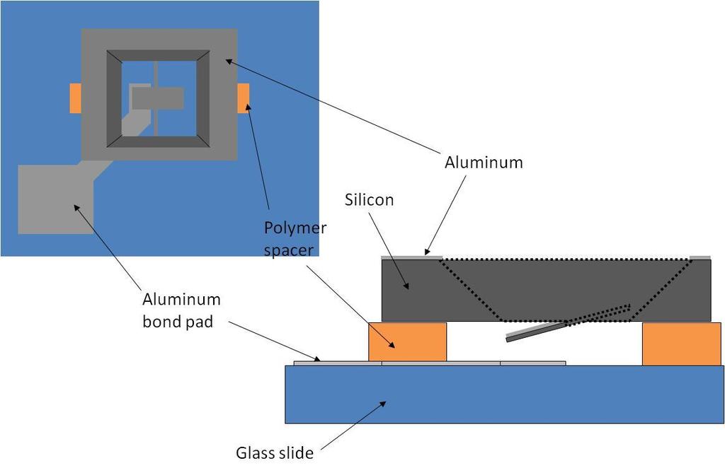
77 67


78 Appendix C SEM Pictures Device Face Hinge 68
79 69
Supplementary Figure 1 Detailed illustration on the fabrication process of templatestripped
 Supplementary Figure 1 Detailed illustration on the fabrication process of templatestripped gold substrate. (a) Spin coating of hydrogen silsesquioxane (HSQ) resist onto the silicon substrate with a thickness
Introduction to Photolithography
 http://www.ichaus.de/news/72 Introduction to Photolithography Photolithography The following slides present an outline of the process by which integrated circuits are made, of which photolithography is
DEPOSITION OF THIN TiO 2 FILMS BY DC MAGNETRON SPUTTERING METHOD
 Chapter 4 DEPOSITION OF THIN TiO 2 FILMS BY DC MAGNETRON SPUTTERING METHOD 4.1 INTRODUCTION Sputter deposition process is another old technique being used in modern semiconductor industries. Sputtering
UNIT 3. By: Ajay Kumar Gautam Asst. Prof. Dev Bhoomi Institute of Technology & Engineering, Dehradun
 UNIT 3 By: Ajay Kumar Gautam Asst. Prof. Dev Bhoomi Institute of Technology & Engineering, Dehradun 1 Syllabus Lithography: photolithography and pattern transfer, Optical and non optical lithography, electron,
percolating nanotube networks
 Supporting Information for: A highly elastic, capacitive strain gauge based on percolating nanotube networks 0.2 0.18 0.16 0.14 Force (kgf) 0.12 0.1 0.08 0.06 0.04 0.02 Raw Data Mooney-Rivlin (R 2 =0.996)
ETCHING Chapter 10. Mask. Photoresist
 ETCHING Chapter 10 Mask Light Deposited Substrate Photoresist Etch mask deposition Photoresist application Exposure Development Etching Resist removal Etching of thin films and sometimes the silicon substrate
Y. C. Lee. Micro-Scale Engineering I Microelectromechanical Systems (MEMS)
") Micro-Scale Engineering I Microelectromechanical Systems (MEMS) Y. C. Lee Department of Mechanical Engineering University of Colorado Boulder, CO 80309-0427 leeyc@colorado.edu January 15, 2014 1 Contents
Micro-Scale Engineering I Microelectromechanical Systems (MEMS) Y. C. Lee Department of Mechanical Engineering University of Colorado Boulder, CO 80309-0427 leeyc@colorado.edu January 15, 2014 1 Contents
Figure 1: Graphene release, transfer and stacking processes. The graphene stacking began with CVD
 Supplementary figure 1 Graphene Growth and Transfer Graphene PMMA FeCl 3 DI water Copper foil CVD growth Back side etch PMMA coating Copper etch in 0.25M FeCl 3 DI water rinse 1 st transfer DI water 1:10
Chapter 3 : ULSI Manufacturing Technology - (c) Photolithography
 Photolithography") Chapter 3 : ULSI Manufacturing Technology - (c) Photolithography 1 Reference 1. Semiconductor Manufacturing Technology : Michael Quirk and Julian Serda (2001) 2. - (2004) 3. Semiconductor Physics and Devices-
Chapter 3 : ULSI Manufacturing Technology - (c) Photolithography 1 Reference 1. Semiconductor Manufacturing Technology : Michael Quirk and Julian Serda (2001) 2. - (2004) 3. Semiconductor Physics and Devices-
Foundations of MEMS. Chang Liu. McCormick School of Engineering and Applied Science Northwestern University. International Edition Contributions by
 Foundations of MEMS Second Edition Chang Liu McCormick School of Engineering and Applied Science Northwestern University International Edition Contributions by Vaishali B. Mungurwadi B. V. Bhoomaraddi
DESIGN, FABRICATION AND ELECTROMECHANICAL CHARACTERISTICS OF A MEMS BASED MICROMIRROR
 XIX IMEKO World Congress Fundamental and Applied Metrology September 6 11, 2009, Lisbon, Portugal DESIGN, FABRICATION AND ELECTROMECHANICAL CHARACTERISTICS OF A MEMS BASED MICROMIRROR Talari Rambabu 1,
Institute for Electron Microscopy and Nanoanalysis Graz Centre for Electron Microscopy
 Institute for Electron Microscopy and Nanoanalysis Graz Centre for Electron Microscopy Micromechanics Ass.Prof. Priv.-Doz. DI Dr. Harald Plank a,b a Institute of Electron Microscopy and Nanoanalysis, Graz
Etching Issues - Anisotropy. Dry Etching. Dry Etching Overview. Etching Issues - Selectivity
 Etching Issues - Anisotropy Dry Etching Dr. Bruce K. Gale Fundamentals of Micromachining BIOEN 6421 EL EN 5221 and 6221 ME EN 5960 and 6960 Isotropic etchants etch at the same rate in every direction mask
Optimizing micromechanical force detectors for measuring. magnetization at high magnetic fields
 Abstract Optimizing micromechanical force detectors for measuring magnetization at high magnetic fields Jeremy Paster University of Florida July 30, 2008 MEMS devices prove to be advantageous in magnetometry.
IC Fabrication Technology
 IC Fabrication Technology * History: 1958-59: J. Kilby, Texas Instruments and R. Noyce, Fairchild * Key Idea: batch fabrication of electronic circuits n entire circuit, say 10 7 transistors and 5 levels
Lecture 6 Plasmas. Chapters 10 &16 Wolf and Tauber. ECE611 / CHE611 Electronic Materials Processing Fall John Labram 1/68
 Lecture 6 Plasmas Chapters 10 &16 Wolf and Tauber 1/68 Announcements Homework: Homework will be returned to you on Thursday (12 th October). Solutions will be also posted online on Thursday (12 th October)
Carrier Transport by Diffusion
 Carrier Transport by Diffusion Holes diffuse ÒdownÓ the concentration gradient and carry a positive charge --> hole diffusion current has the opposite sign to the gradient in hole concentration dp/dx p(x)
Lecture 150 Basic IC Processes (10/10/01) Page ECE Analog Integrated Circuits and Systems P.E. Allen
 Page ECE Analog Integrated Circuits and Systems P.E. Allen") Lecture 150 Basic IC Processes (10/10/01) Page 1501 LECTURE 150 BASIC IC PROCESSES (READING: TextSec. 2.2) INTRODUCTION Objective The objective of this presentation is: 1.) Introduce the fabrication of
Lecture 150 Basic IC Processes (10/10/01) Page 1501 LECTURE 150 BASIC IC PROCESSES (READING: TextSec. 2.2) INTRODUCTION Objective The objective of this presentation is: 1.) Introduce the fabrication of
2.76/2.760 Multiscale Systems Design & Manufacturing
 2.76/2.760 Multiscale Systems Design & Manufacturing Fall 2004 MOEMS Devices for Optical communications system Switches and micromirror for Add/drops Diagrams removed for copyright reasons. MOEMS MEMS
MEMS Tuning-Fork Gyroscope Mid-Term Report Amanda Bristow Travis Barton Stephen Nary
 MEMS Tuning-Fork Gyroscope Mid-Term Report Amanda Bristow Travis Barton Stephen Nary Abstract MEMS based gyroscopes have gained in popularity for use as rotation rate sensors in commercial products like
Dry Etching Zheng Yang ERF 3017, MW 5:15-6:00 pm
 Dry Etching Zheng Yang ERF 3017, email: yangzhen@uic.edu, MW 5:15-6:00 pm Page 1 Page 2 Dry Etching Why dry etching? - WE is limited to pattern sizes above 3mm - WE is isotropic causing underetching -
Kavli Workshop for Journalists. June 13th, CNF Cleanroom Activities
 Kavli Workshop for Journalists June 13th, 2007 CNF Cleanroom Activities Seeing nm-sized Objects with an SEM Lab experience: Scanning Electron Microscopy Equipment: Zeiss Supra 55VP Scanning electron microscopes
UNIVERSITY OF CALIFORNIA College of Engineering Department of Electrical Engineering and Computer Sciences. Fall Exam 1
 UNIVERSITY OF CALIFORNIA College of Engineering Department of Electrical Engineering and Computer Sciences EECS 143 Fall 2008 Exam 1 Professor Ali Javey Answer Key Name: SID: 1337 Closed book. One sheet
Thin Wafer Handling Challenges and Emerging Solutions
 1 Thin Wafer Handling Challenges and Emerging Solutions Dr. Shari Farrens, Mr. Pete Bisson, Mr. Sumant Sood and Mr. James Hermanowski SUSS MicroTec, 228 Suss Drive, Waterbury Center, VT 05655, USA 2 Thin
LECTURE 5 SUMMARY OF KEY IDEAS
 LECTURE 5 SUMMARY OF KEY IDEAS Etching is a processing step following lithography: it transfers a circuit image from the photoresist to materials form which devices are made or to hard masking or sacrificial
1. Narrative Overview Questions
 Homework 4 Due Nov. 16, 010 Required Reading: Text and Lecture Slides on Downloadable from Course WEB site: http://courses.washington.edu/overney/nme498.html 1. Narrative Overview Questions Question 1
Etching: Basic Terminology
 Lecture 7 Etching Etching: Basic Terminology Introduction : Etching of thin films and sometimes the silicon substrate are very common process steps. Usually selectivity, and directionality are the first
CHAPTER 6: Etching. Chapter 6 1
 Chapter 6 1 CHAPTER 6: Etching Different etching processes are selected depending upon the particular material to be removed. As shown in Figure 6.1, wet chemical processes result in isotropic etching
MICROCHIP MANUFACTURING by S. Wolf
 by S. Wolf Chapter 15 ALUMINUM THIN-FILMS and SPUTTER-DEPOSITION 2004 by LATTICE PRESS CHAPTER 15 - CONTENTS Aluminum Thin-Films Sputter-Deposition Process Steps Physics of Sputter-Deposition Magnetron-Sputtering
A Novel Approach to the Layer Number-Controlled and Grain Size- Controlled Growth of High Quality Graphene for Nanoelectronics
 Supporting Information A Novel Approach to the Layer Number-Controlled and Grain Size- Controlled Growth of High Quality Graphene for Nanoelectronics Tej B. Limbu 1,2, Jean C. Hernández 3, Frank Mendoza
Wet and Dry Etching. Theory
 Wet and Dry Etching Theory 1. Introduction Etching techniques are commonly used in the fabrication processes of semiconductor devices to remove selected layers for the purposes of pattern transfer, wafer
nmos IC Design Report Module: EEE 112
 nmos IC Design Report Author: 1302509 Zhao Ruimin Module: EEE 112 Lecturer: Date: Dr.Zhao Ce Zhou June/5/2015 Abstract This lab intended to train the experimental skills of the layout designing of the
4FNJDPOEVDUPS 'BCSJDBUJPO &UDI
 2010.5.4 1 Major Fabrication Steps in CMOS Process Flow UV light oxygen Silicon dioxide Silicon substrate Oxidation (Field oxide) photoresist Photoresist Coating Mask exposed photoresist Mask-Wafer Exposed
Fast Bonding of Substrates for the Formation of Microfluidic Channels at Room Temperature
 Supplementary Material (ESI) for Lab on a Chip This journal is The Royal Society of Chemistry 2005 Supporting Information Fast Bonding of Substrates for the Formation of Microfluidic Channels at Room Temperature
Basic Laboratory. Materials Science and Engineering. Atomic Force Microscopy (AFM)
") Basic Laboratory Materials Science and Engineering Atomic Force Microscopy (AFM) M108 Stand: 20.10.2015 Aim: Presentation of an application of the AFM for studying surface morphology. Inhalt 1.Introduction...
Basic Laboratory Materials Science and Engineering Atomic Force Microscopy (AFM) M108 Stand: 20.10.2015 Aim: Presentation of an application of the AFM for studying surface morphology. Inhalt 1.Introduction...
Supplementary Materials for
 advances.sciencemag.org/cgi/content/full/3/9/e1701222/dc1 Supplementary Materials for Moisture-triggered physically transient electronics Yang Gao, Ying Zhang, Xu Wang, Kyoseung Sim, Jingshen Liu, Ji Chen,
SUPPLEMENTARY FIGURES
 SUPPLEMENTARY FIGURES a b c Supplementary Figure 1 Fabrication of the near-field radiative heat transfer device. a, Main fabrication steps for the bottom Si substrate. b, Main fabrication steps for the
Fabrication Technology, Part I
 EEL5225: Principles of MEMS Transducers (Fall 2004) Fabrication Technology, Part I Agenda: Microfabrication Overview Basic semiconductor devices Materials Key processes Oxidation Thin-film Deposition Reading:
Bending Load & Calibration Module
 Bending Load & Calibration Module Objectives After completing this module, students shall be able to: 1) Conduct laboratory work to validate beam bending stress equations. 2) Develop an understanding of
EE 527 MICROFABRICATION. Lecture 24 Tai-Chang Chen University of Washington
 EE 527 MICROFABRICATION Lecture 24 Tai-Chang Chen University of Washington EDP ETCHING OF SILICON - 1 Ethylene Diamine Pyrocatechol Anisotropy: (100):(111) ~ 35:1 EDP is very corrosive, very carcinogenic,
Introduction to Actuators PK
 Introduction to Actuators Primary Knowledge Participant Guide Description and Estimated Time to Complete This learning module is one of three SCME modules that discuss the types of components found in
Self-study problems and questions Processing and Device Technology, FFF110/FYSD13
 Self-study problems and questions Processing and Device Technology, FFF110/FYSD13 Version 2016_01 In addition to the problems discussed at the seminars and at the lectures, you can use this set of problems
EE 527 MICROFABRICATION. Lecture 25 Tai-Chang Chen University of Washington
 EE 527 MICROFABRICATION Lecture 25 Tai-Chang Chen University of Washington ION MILLING SYSTEM Kaufmann source Use e-beam to strike plasma A magnetic field applied to increase ion density Drawback Low etch
1
 Process methodologies for temporary thin wafer handling solutions By Justin Furse, Technology Strategist, Brewer Science, Inc. Use of temporary bonding/debonding as part of thin wafer handling processes
CHAPTER 5 FIXED GUIDED BEAM ANALYSIS
 77 CHAPTER 5 FIXED GUIDED BEAM ANALYSIS 5.1 INTRODUCTION Fixed guided clamped and cantilever beams have been designed and analyzed using ANSYS and their performance were calculated. Maximum deflection
MODELING OF T-SHAPED MICROCANTILEVER RESONATORS. Margarita Narducci, Eduard Figueras, Isabel Gràcia, Luis Fonseca, Joaquin Santander, Carles Cané
 Stresa, Italy, 5-7 April 007 MODELING OF T-SHAPED MICROCANTILEVER RESONATORS Margarita Narducci, Eduard Figueras, Isabel Gràcia, Luis Fonseca, Joaquin Santander, Carles Centro Nacional de Microelectrónica
Lithography and Etching
 Lithography and Etching Victor Ovchinnikov Chapters 8.1, 8.4, 9, 11 Previous lecture Microdevices Main processes: Thin film deposition Patterning (lithography) Doping Materials: Single crystal (monocrystal)
Pattern Transfer- photolithography
 Pattern Transfer- photolithography DUV : EUV : 13 nm 248 (KrF), 193 (ArF), 157 (F 2 )nm H line: 400 nm I line: 365 nm G line: 436 nm Wavelength (nm) High pressure Hg arc lamp emission Ref: Campbell: 7
Hopping in CVD Grown Single-layer MoS 2
 Supporting Information for Large Thermoelectricity via Variable Range Hopping in CVD Grown Single-layer MoS 2 Jing Wu 1,2,3, Hennrik Schmidt 1,2, Kiran Kumar Amara 4, Xiangfan Xu 5, Goki Eda 1,2,4, and
Electromechanical Sensors and Actuators Fall Term
 Electromechanical Sensors and Actuators Dr. Qing-Ming Wang Professor of Mechanical Engineering and Materials Science University of Pittsburgh 2017 Fall Term Lecture 1 Introduction and Transducer Models
Lecture 0: Introduction
 Lecture 0: Introduction Introduction q Integrated circuits: many transistors on one chip q Very Large Scale Integration (VLSI): bucketloads! q Complementary Metal Oxide Semiconductor Fast, cheap, low power
Metal Deposition. Filament Evaporation E-beam Evaporation Sputter Deposition
 Metal Deposition Filament Evaporation E-beam Evaporation Sputter Deposition 1 Filament evaporation metals are raised to their melting point by resistive heating under vacuum metal pellets are placed on
SCME KIT OVERVIEW. Rainbow Wafer Kit
 SCME KIT OVERVIEW Rainbow Wafer Kit Micro Nano Conference I - 2011 Objectives of Each Kit The SCME kits are designed to work both as a stand-alone activity as well as to support the materials introduced
EE C245 ME C218 Introduction to MEMS Design Fall 2007
 EE C245 ME C218 Introduction to MEMS Design Fall 2007 Prof. Clark T.-C. Nguyen Dept. of Electrical Engineering & Computer Sciences University of California at Berkeley Berkeley, CA 94720 Lecture 12: Mechanics
Section 3: Etching. Jaeger Chapter 2 Reader
 Section 3: Etching Jaeger Chapter 2 Reader Etch rate Etch Process - Figures of Merit Etch rate uniformity Selectivity Anisotropy d m Bias and anisotropy etching mask h f substrate d f d m substrate d f
E SC 412 Nanotechnology: Materials, Infrastructure, and Safety Wook Jun Nam
 E SC 412 Nanotechnology: Materials, Infrastructure, and Safety Wook Jun Nam Lecture 10 Outline 1. Wet Etching/Vapor Phase Etching 2. Dry Etching DC/RF Plasma Plasma Reactors Materials/Gases Etching Parameters
Introduction to Microeletromechanical Systems (MEMS) Lecture 9 Topics. MEMS Overview
 Lecture 9 Topics. MEMS Overview") Introduction to Microeletromechanical Systems (MEMS) Lecture 9 Topics MicroOptoElectroMechanical Systems (MOEMS) Grating Light Valves Corner Cube Reflector (CCR) MEMS Light Modulator Optical Switch Micromirrors
Introduction to Microeletromechanical Systems (MEMS) Lecture 9 Topics MicroOptoElectroMechanical Systems (MOEMS) Grating Light Valves Corner Cube Reflector (CCR) MEMS Light Modulator Optical Switch Micromirrors
Sensors and Transducers. mywbut.com
 Sensors and Transducers 1 Objectives At the end of this chapter, the students should be able to: describe the principle of operation of various sensors and transducers; namely.. Resistive Position Transducers.
b. The displacement of the mass due to a constant acceleration a is x=
 EE147/247A Final, Fall 2013 Page 1 /35 2 /55 NO CALCULATORS, CELL PHONES, or other electronics allowed. Show your work, and put final answers in the boxes provided. Use proper units in all answers. 1.
Transducers. ME 3251 Thermal Fluid Systems
 Transducers ME 3251 Thermal Fluid Systems 1 Transducers Transform values of physical variables into equivalent electrical signals Converts a signal from one form to another form 2 Types of Transducers
Thermal Resistance Measurement
 Optotherm, Inc. 2591 Wexford-Bayne Rd Suite 304 Sewickley, PA 15143 USA phone +1 (724) 940-7600 fax +1 (724) 940-7611 www.optotherm.com Optotherm Sentris/Micro Application Note Thermal Resistance Measurement
TE 75R RESEARCH RUBBER FRICTION TEST MACHINE
 TE 75R RESEARCH RUBBER FRICTION TEST MACHINE Background: The Research Rubber Friction Test Machine offers the ability to investigate fully the frictional behaviour of rubbery materials both in dry and
Passionately Innovating With Customers To Create A Connected World
 Passionately Innovating With Customers To Create A Connected World Multi Die Integration Can Material Suppliers Meet the Challenge? Nov 14, 2012 Jeff Calvert - R&D Director, Advanced Packaging Technologies
Lecture 11. Etching Techniques Reading: Chapter 11. ECE Dr. Alan Doolittle
 Lecture 11 Etching Techniques Reading: Chapter 11 Etching Techniques Characterized by: 1.) Etch rate (A/minute) 2.) Selectivity: S=etch rate material 1 / etch rate material 2 is said to have a selectivity
Integrating MEMS Electro-Static Driven Micro-Probe and Laser Doppler Vibrometer for Non-Contact Vibration Mode SPM System Design
 Tamkang Journal of Science and Engineering, Vol. 12, No. 4, pp. 399 407 (2009) 399 Integrating MEMS Electro-Static Driven Micro-Probe and Laser Doppler Vibrometer for Non-Contact Vibration Mode SPM System
EE C245 ME C218 Introduction to MEMS Design Fall 2007
 EE C245 ME C218 Introduction to MEMS Design Fall 2007 Prof. Clark T.-C. Nguyen Dept. of Electrical Engineering & Computer Sciences University of California at Berkeley Berkeley, CA 94720 Lecture 11: Bulk
INTRODUCTION Strained Silicon Monochromator Magnesium Housing Windows for Monochromator Shutter and Collimator Fission Detector HOPG Monochromator
 Design for a Four-Blade Neutron Interferometer INTRODUCTION Strained Silicon Monochromator The neutron beam used for this interferometer is separated from the NIST reactor's main beam using a strained
Carbonized Electrospun Nanofiber Sheets for Thermophones
 Supporting Information Carbonized Electrospun Nanofiber Sheets for Thermophones Ali E. Aliev 1 *, Sahila Perananthan 2, John P. Ferraris 1,2 1 A. G. MacDiarmid NanoTech Institute, University of Texas at
Case Study of Electronic Materials Packaging with Poor Metal Adhesion and the Process for Performing Root Cause Failure Analysis
 Case Study of Electronic Materials Packaging with Poor Metal Adhesion and the Process for Performing Root Cause Failure Analysis Dr. E. A. Leone BACKGRUND ne trend in the electronic packaging industry
6.5 Optical-Coating-Deposition Technologies
 92 Chapter 6 6.5 Optical-Coating-Deposition Technologies The coating process takes place in an evaporation chamber with a fully controlled system for the specified requirements. Typical systems are depicted
CHAPTER 4 DESIGN AND ANALYSIS OF CANTILEVER BEAM ELECTROSTATIC ACTUATORS
 61 CHAPTER 4 DESIGN AND ANALYSIS OF CANTILEVER BEAM ELECTROSTATIC ACTUATORS 4.1 INTRODUCTION The analysis of cantilever beams of small dimensions taking into the effect of fringing fields is studied and
SCB10H Series Pressure Elements PRODUCT FAMILY SPEFICIFATION. Doc. No B
 PRODUCT FAMILY SPEFICIFATION SCB10H Series Pressure Elements SCB10H Series Pressure Elements Doc. No. 82 1250 00 B Table of Contents 1 General Description... 3 1.1 Introduction... 3 1.2 General Description...
Supplementary Information. Rapid Stencil Mask Fabrication Enabled One-Step. Polymer-Free Graphene Patterning and Direct
 Supplementary Information Rapid Stencil Mask Fabrication Enabled One-Step Polymer-Free Graphene Patterning and Direct Transfer for Flexible Graphene Devices Keong Yong 1,, Ali Ashraf 1,, Pilgyu Kang 1,
Instrumentation and Operation
 Instrumentation and Operation 1 STM Instrumentation COMPONENTS sharp metal tip scanning system and control electronics feedback electronics (keeps tunneling current constant) image processing system data
Superconducting-Insulating Quantum Phase Transition in Homogenous Thin Films
 Superconducting-Insulating Quantum Phase Transition in Homogenous Thin Films Jonathan K. Whitmer Department of Physics, University of Illinois at Urbana-Champaign 1110 West Green Street, Urbana, IL 61801,
Lecture 19. Measurement of Solid-Mechanical Quantities (Chapter 8) Measuring Strain Measuring Displacement Measuring Linear Velocity
 Measuring Strain Measuring Displacement Measuring Linear Velocity") MECH 373 Instrumentation and Measurements Lecture 19 Measurement of Solid-Mechanical Quantities (Chapter 8) Measuring Strain Measuring Displacement Measuring Linear Velocity Measuring Accepleration and
MECH 373 Instrumentation and Measurements Lecture 19 Measurement of Solid-Mechanical Quantities (Chapter 8) Measuring Strain Measuring Displacement Measuring Linear Velocity Measuring Accepleration and
STRAIN GAUGES YEDITEPE UNIVERSITY DEPARTMENT OF MECHANICAL ENGINEERING
 STRAIN GAUGES YEDITEPE UNIVERSITY DEPARTMENT OF MECHANICAL ENGINEERING 1 YEDITEPE UNIVERSITY ENGINEERING FACULTY MECHANICAL ENGINEERING LABORATORY 1. Objective: Strain Gauges Know how the change in resistance
Selective Manipulation of Molecules by Electrostatic Force and Detection of Single Molecules in Aqueous Solution
 Supporting Information Selective Manipulation of Molecules by Electrostatic Force and Detection of Single Molecules in Aqueous Solution Zhongbo Yan, Ming Xia, Pei Zhang, and Ya-Hong Xie* Department of
Too many answers to list.
 ECE/ME 9 Spring 08, Prof. Feinerman, Test # solutions 5/6/08, Closed Book and Closed Notes Undergraduates x 8.5, σ 1.0, Graduates x 78.5, σ 1. Element Molecular weight, grams Atomic number Density, gm/cc
SURFACE TENSION POWERED SELF-ASSEMBLY OF 3D MOEMS DEVICES USING DRIE OF BONDED SILICON-ON-INSULATOR WAFERS INTRODUCTION
 SURFACE TENSION POWERED SELF-ASSEMBLY OF 3D MOEMS DEVICES USING DRIE OF BONDED SILICON-ON-INSULATOR WAFERS R.R.A Syms, C. Gormley and S. Blackstone Dept. of Electrical and Electronic Engineering, Imperial
Structuring and bonding of glass-wafers. Dr. Anke Sanz-Velasco
 Structuring and bonding of glass-wafers Dr. Anke Sanz-Velasco Outline IMT Why glass? Components for life science Good bond requirements and evaluation Wafer bonding 1. Fusion bonding 2. UV-adhesive bonding
Regents of the University of California
 Deep Reactive-Ion Etching (DRIE) DRIE Issues: Etch Rate Variance The Bosch process: Inductively-coupled plasma Etch Rate: 1.5-4 μm/min Two main cycles in the etch: Etch cycle (5-15 s): SF 6 (SF x+ ) etches
Introduction to Electron Beam Lithography
 Introduction to Electron Beam Lithography Boštjan Berčič (bostjan.bercic@ijs.si), Jožef Štefan Institute, Jamova 39, 1000 Ljubljana, Slovenia 1. Introduction Electron Beam Lithography is a specialized
Temporary Wafer Bonding - Key Technology for 3D-MEMS Integration
 Temporary Wafer Bonding - Key Technology for 3D-MEMS Integration 2016-06-15, Chemnitz Chemnitz University of Technology Basic Research Fraunhofer ENAS System-Packaging (SP) Back-End of Line (BEOL) Applied
EE C245 / ME C218 INTRODUCTION TO MEMS DESIGN FALL 2009 PROBLEM SET #7. Due (at 7 p.m.): Thursday, Dec. 10, 2009, in the EE C245 HW box in 240 Cory.
: Thursday, Dec. 10, 2009, in the EE C245 HW box in 240 Cory.") Issued: Thursday, Nov. 24, 2009 PROBLEM SET #7 Due (at 7 p.m.): Thursday, Dec. 10, 2009, in the EE C245 HW box in 240 Cory. 1. Gyroscopes are inertial sensors that measure rotation rate, which is an extremely
Issued: Thursday, Nov. 24, 2009 PROBLEM SET #7 Due (at 7 p.m.): Thursday, Dec. 10, 2009, in the EE C245 HW box in 240 Cory. 1. Gyroscopes are inertial sensors that measure rotation rate, which is an extremely
Piezo Theory: Chapter 1 - Physics & Design
 Piezoelectric effect inverse piezoelectric effect The result of external forces to a piezoelectric material is positive and negative electrical charges at the surface of the material. If electrodes are
Lecture 18: Microfluidic MEMS, Applications
 MECH 466 Microelectromechanical Systems University of Victoria Dept. of Mechanical Engineering Lecture 18: Microfluidic MEMS, Applications 1 Overview Microfluidic Electrokinetic Flow Basic Microfluidic
Methods. Casting Mold Fabrication. Channel Fabrication. Sample assembly
 Methods Casting Mold Fabrication We fabricated the ratchet devices using the polydimethylsiloxane (PDMS) rapid prototyping technique. Photolithography chrome masks (3" plates, Nanofilm) were patterned
PIEZOELECTRIC TECHNOLOGY PRIMER
 PIEZOELECTRIC TECHNOLOGY PRIMER James R. Phillips Sr. Member of Technical Staff CTS Wireless Components 4800 Alameda Blvd. N.E. Albuquerque, New Mexico 87113 Piezoelectricity The piezoelectric effect is
Performance Evaluation of Polymers for Bumping and Wafer Level Packaging
 Performance Evaluation of Polymers for Bumping and Wafer Level Packaging John JH Reche 945 E. Verde Lane, Tempe, AZ 85284 jjhreche@wafer-bumping.com 11th Symposium on Wintherthur Museum and Gardens, DE
Outline. 4 Mechanical Sensors Introduction General Mechanical properties Piezoresistivity Piezoresistive Sensors Capacitive sensors Applications
 Sensor devices Outline 4 Mechanical Sensors Introduction General Mechanical properties Piezoresistivity Piezoresistive Sensors Capacitive sensors Applications Introduction Two Major classes of mechanical
Supplementary materials for: Large scale arrays of single layer graphene resonators
 Supplementary materials for: Large scale arrays of single layer graphene resonators Arend M. van der Zande* 1, Robert A. Barton 2, Jonathan S. Alden 2, Carlos S. Ruiz-Vargas 2, William S. Whitney 1, Phi
SUPPLEMENTARY NOTES Supplementary Note 1: Fabrication of Scanning Thermal Microscopy Probes
 SUPPLEMENTARY NOTES Supplementary Note 1: Fabrication of Scanning Thermal Microscopy Probes Fabrication of the scanning thermal microscopy (SThM) probes is summarized in Supplementary Fig. 1 and proceeds
Design of Electrostatic Actuators for MOEMS Applications
 Design of Electrostatic Actuators for MOEMS Applications Dooyoung Hah 1,, Hiroshi Toshiyoshi 1,3, and Ming C. Wu 1 1 Department of Electrical Engineering, University of California, Los Angeles Box 951594,
Top down and bottom up fabrication
 Lecture 24 Top down and bottom up fabrication Lithography ( lithos stone / graphein to write) City of words lithograph h (Vito Acconci, 1999) 1930 s lithography press Photolithography d 2( NA) NA=numerical
MICROELECTROMECHANICAL system (MEMS)
") JOURNAL OF MICROELECTROMECHANICAL SYSTEMS, VOL. 13, NO. 1, FEBRUARY 2004 51 Electrostatic Actuators With Expanded Tuning Range Due to Biaxial Intrinsic Stress Gradients Gary D. Gray, Matthew J. Morgan,
JOURNAL OF MICROELECTROMECHANICAL SYSTEMS, VOL. 13, NO. 1, FEBRUARY 2004 51 Electrostatic Actuators With Expanded Tuning Range Due to Biaxial Intrinsic Stress Gradients Gary D. Gray, Matthew J. Morgan,
Plasmonic Hot Hole Generation by Interband Transition in Gold-Polyaniline
 Supplementary Information Plasmonic Hot Hole Generation by Interband Transition in Gold-Polyaniline Tapan Barman, Amreen A. Hussain, Bikash Sharma, Arup R. Pal* Plasma Nanotech Lab, Physical Sciences Division,
SUPPORTING INFORMATION. Si wire growth. Si wires were grown from Si(111) substrate that had a low miscut angle
 substrate that had a low miscut angle") SUPPORTING INFORMATION The general fabrication process is illustrated in Figure 1. Si wire growth. Si wires were grown from Si(111) substrate that had a low miscut angle of 0.1. The Si was covered with
SUPPORTING INFORMATION The general fabrication process is illustrated in Figure 1. Si wire growth. Si wires were grown from Si(111) substrate that had a low miscut angle of 0.1. The Si was covered with
Nanotechnology Fabrication Methods.
 Nanotechnology Fabrication Methods. 10 / 05 / 2016 1 Summary: 1.Introduction to Nanotechnology:...3 2.Nanotechnology Fabrication Methods:...5 2.1.Top-down Methods:...7 2.2.Bottom-up Methods:...16 3.Conclusions:...19
10 Measurement of Acceleration, Vibration and Shock Transducers
 Chapter 10: Acceleration, Vibration and Shock Measurement Dr. Lufti Al-Sharif (Revision 1.0, 25/5/2008) 1. Introduction This chapter examines the measurement of acceleration, vibration and shock. It starts