Scanning tunneling microscope. STM: Looking to atoms atomic resolution. STM tip. 1981: Gerld Binnig, Heinrich Röhrer. Nobel Prize 1986 IBM - Zurich
|
|
|
- Elisabeth Holt
- 5 years ago
- Views:
Transcription


1 Scanning tunneling microscope 1nA STM tip 0.001nA 0.1nm 1nm Tip-surface distance 1981: Gerld Binnig, Heinrich Röhrer Si surface Cu surface Nobel Prize 1986 IBM - Zurich STM: Looking to atoms atomic resolution Image LPM 15 nm X 10 millions Image LPM 1.5 nm X 100 millions
.")
2 Moving atoms one by one by STM Title : The Beginning 1988 Donald Eigler IBM Xenon on Nickel (110) Artists have almost always needed the support of patrons (scientists too!). Here, the artist, shortly after discovering how to move atoms with the STM, found a way to give something back to the corporation which gave him a job when he needed one and provided him with the tools he needed in order to be successful.

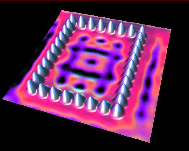
3 2D finite potential well =» QUANTUM CORAL To make this image, 48 iron atoms (shown as yellow peaks) were placed in a circle on a copper surface. The elevation at each point inside the circle indicates the electron density within the circle. The standing wave pattern is very similar to the probability distribution function for a particle in a one dimensional finite potential well: e ( x, y) 2 IBM M.F. Crommie, C.P. Lutz, D.M. Eigler, Science 262, (1993).

4 Quantum corrals

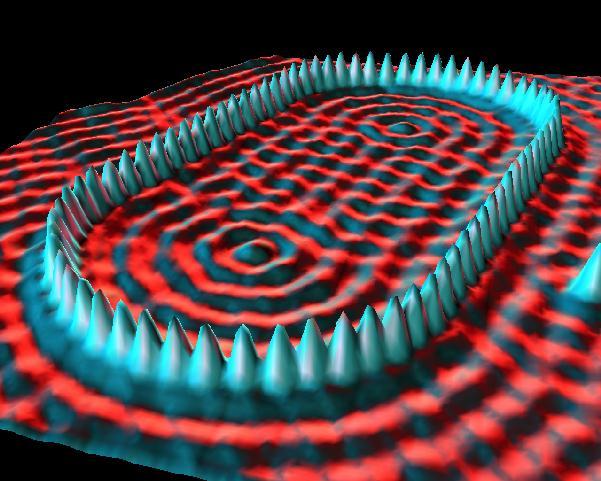
5 Reminiscent of formal Japanese rock gardens, here we see ripples surrounding features on the copper (111) surface. The artists' fortunes took a major turn upward when they determined that the ripples were due to "surface state electrons." These electrons are free to roam about the surface but not to penetrate into the solid. When one of these electrons encounters an obstacle like a step edge, it is partially reflected. The ripples extending away from the step edges and the various defects in the crystal surface are just the standing waves that are created whenever a wave scatters off of something. The standing waves are about 15 Angstroms (roughly 10 atomic diameters) from crest to crest. The amplitude is largest adjacent to the step edge where it is about 0.04 Angstroms from crest to trough.

6 Quantum mirage 36 cobalt atoms in an elliptical structure known as a "quantum corral." Electron waves moving in the copper substrate interact both with a magnetic cobalt atom carefully positioned at one of the foci of the ellipse and apparently with a "mirage" of another cobalt atom (that isn't really there) at the other focus. Donald Eigler IBM Almaden
 U() r 2 e 4 r 0 Legatura coordonate")
 2m 2 2 2 2 2 2 x y z Operatorul Laplace (x,y,z) se poate transforma/scrie in coordonate sferice (r,, ) 2 1 2 1 1")
7 ATOMUL DE HIDROGEN Energia potentiala a electronului care se misca in jurul nucleului are simetrie sferica, depinzand doar de distanta: r x y z Coordonate sferice: (r,, ) U() r 2 e 4 r 0 Legatura coordonate cartezienecoordonate sferice x rcos sin y rsin sin z rcos Ecuatia Schrodinger 3D Hˆ (r,, ) E (r,, ) 2 ˆ H U( x, y, z) 2m x y z Operatorul Laplace (x,y,z) se poate transforma/scrie in coordonate sferice (r,, ) r sin 2 2 r r r sin sin
.")

8 Ecuatia lui Schrödinger pentru atomul de hidrogen Hˆ (r,, ) E (r,, ) Stari stationare ale electronului in atomul de hidrogen Intr o dimensiune, cuantificarea anergiei apare ca si o consecinta a conditiilor la limita a functiei de unda (restrangerii spatiale). Aceasta implica faptul ca doar pentru anumite valori discrete ale energiei, caracterizate de numarul cuantic n, solutiile ecuatie Schodinger satisfac conditiile la limita. In 3 Dimensiuni, functia de unda trebuie sa satisfaca 3 conditii limita diferite. In consecinta, solutia ecuatiei lui Schrodinger 3D va fi caracterizata de 3 numere cuantice care fiecare va cuantifica o marime fizica distincta. Numar cuantic principal Numar cuantic orbital Numar cuantic magnetic
 Trebuie sa fie finita in in 0 si Modulul momentului cinetic orbital 3.")
9 1. Cuantificarea energiei totale n = Numar cuantic principal Nivele de energie ale H 2. Cuantificarea momentului cinetic orbital Origind: conditia la limita l numar cuantic orbital ( ) Trebuie sa fie finita in in 0 si Modulul momentului cinetic orbital 3. Cuantificarea componentei momentului cinetic orbital pe o anumita directie (ex. L z directia aplicarii unui camp magnetic) Origine: conditie limita periodica m l = numar cuantic magnetic ( ) ( 2 ) Componenta z a momentului cinetic orbital
 l 2 Distributii de probabilitate 3D pentru cateva stari cuantice ale atomului de")
10 Stari cuantice ale atomului de Hidrogen Notatie spectroscopica Stratul etc Distributia de probabilitate a prezentei electcronului/orbitali,, (, r nlm, ) l 2 Distributii de probabilitate 3D pentru cateva stari cuantice ale atomului de H
11 Spinul electronului Efectul Zeeman consta in despicarea nivelelor de energie atomice si a liniilor spectrale asociate cand atomul este plasat intr un camp magnetic extern. Momentul magnetic orbital al electronului Cand un dipol magnetic de moment este plasat intr un camp magnetic B energia potentiala de interactiune va fi: Daca B este orientat de a lungul axei oz Energie de interactiune magnetica orbitala

12 Despicarea Zeeman Campul magnetic decaleaza energia fiecarei stari orbitale cu o cantitate U. Energia de interactiune U depinde de valoarea lui m l deoarece m l determina orientarea momentului magnetic orbital relativa la campul magnetic. Valorile lui m l sunt cuprinse intre l to l in pasi de unu, deci un nivel de energie cu o valoare particulara a numarului cuantic orbital contine (2l+1) stari orbitale diferite. In absenta unui camp magnetic extern aceste stari au toate aceasi energie (degenerate). Campul magnetic ridica degenerarea: in prezenta campului magnetic fiecare nivel de energie degenerat este separat in (2l+1) nivele distincte; l=1 despicat in 2X1+1=3 l=0 nu este despicat

13 Experimentul Stern Gerlach La inceputul anilor 1920, fizicienii germani Otto Stern si Walter Gerlach dezvolta o tehnica pentru masurarea momentului magnetic al atomilor. Dispozitivul lor prepara un fascicul atomic evaporand atomi intr un cuptor din care pot iesi printr un orificiu ingust. Acesti atom se deplaseaza in vid traversand un sector de camp magnetic neuniform (gradient de camp obtinut prin forma polilor magnetilor). Reducand marimea polului superior conduce la un cam magnetic mai puternic la polul superior. Ecran colector Atomi cu polul nord in sus in sus sunt deflectati in sus Fascicul atomic colimat Cuptor Colimator B crescator F z B z z Campul magnetic neuniform este mai puternic la polul Sud al magnetului. Extremitatea dipolului magnetic mai aporoape de polul sud simte o forta mai mare. Atomi cu polul sud in sus sunt deflectati in jos


14 Forta Fz B z e L B e z ml B z 2m z 2m z Observatie experimentala: Ecran colector Magnet oprit: camp magnetiz zero, toti atomii cu l=0 ajung in centru Magnet pornit: camp magnetic diferit de zero, atomii cu l=1 au trei valori Lz conduc la 3 spoturi In 1927, odata dezvoltata teoria cuantica a lui Schrödinger, tehnica Stern Gerlach a fost folosita pentru masurarea momentului magnetic al atomilor de hidrogen. Starea fundamentala a atomului de hidrogen este 1s, cu l = 0, astfel incat atomul nu ar trebui sa aiba mamoment magnetic deci nu ar trebui sa se observe deflectie deloc. Centru ecranului colector In realitate experimentul demostreaza o despicare in doua a fascicolului.

15 O explicare a acestor observatii a fost sugerata si apoi confirmata ulterior: electronul are un moment magnetic intrinsec. In consecinta el are si un moment cinetic intrinsec. Acest moment cinetic propriu intrinsec este numit spin S Experimentul Stern Gerlach ne spune ca componenta z a momentului cinetic de spin poate lua doar doua valori: m s = numar cuantic magnetic de spin Starea ms 1 2 cu 1 Sz Se numeste stare SPIN UP 2 Starea 1 ms 2 cu 1 Sz Se numeste stare SPIN DOWN 2 Analog cuantificarii modului momentului cinetic orbital, avem si aici: S s( s 1) cu s =1/2 numar cuantic de spin Moment cinetic de spin
16 Spinul electronului are implicatii semnificative pentru structura atomului. Solutiile ecuatiei Schrödinger pot fi descrise de trei numere cuantice n, l, sim, insa experimentul Stern Gerlach ne arata faptul ca aceasta nu este o descrierer completa a atomului. In realitate avem nevoie de patru numere cuantice (n, l, m l, m s ) pentru a caracteriza o stare stationara a atomului. Orientarea spinului nu afecteaza energia atomului, astfel incat in starea fundamentala electronul poate fi ori in stare spin up (1,0,0,+1/2) or in stare spin down (1,0,0, 1/2). Recapitulare Numar cuantic Simbol Valori permise Descrie/cuantifica Principal n 1,2,3, Distanta fata de nucleu/energia totala Orbital l 0,1,2,(n 1) Momentul cinetic orbital Magnetic orbital m l 0, 1, 2,, l Componenta z a momentului cinetic orbital Spin s 1/2 Momentul cinetic de spin Magnetic de spin m s 1/2 Componenta z a momentului cinetic de spin


17 SPINTRONICS Electron S Electron = charge + spin e spin electronics magnetism Charge Purpose of spin-electronics: combine electronics and magnetism in order to make new devices in which both the charge and the spin of the electron play an active role ``Teaching electrons new tricks by manipulating the electron spin in solid state electronic devices

 in")


18 SPINTRONICS: excellence research area Nobel Prize Physics : The giant magnetorezistance (GMR) in magnetic multilayers Baibich et al. Phys. Rev. Lett. 61 (1988) 2472 G. Binash et al., Phys. Rev. B, 39, 4828 (1989) Race track
")

 10,4 10,2")

, 0 60 120 180")

 0 8-300 0 300 Magnetic")

19 SPINTRONIC DEVICES CIP Sensors : field, position (compass, ABS, ) Read heads HDD Nonvolatile memories HF oscillators Logic elements CPP Current I=f( ) spin valve effect R (ohms) 10,4 10,2 10,0 9,8 9,6 9,4 Si/SiO2//Ta/NiFe/CoFe/Cu/CoFe/IrMn Theta (deg) R R R R R 2 2 θ M, M ) P AP P AP 1 2 cos(θ), Si/SiO2//Ta/Co2FeAl/MgO/CoFe/IrMn Rezistenta (k ) (1) (0) Magnetic field(oe) R 100 TMR(%) SPINTRONIC: POS CCE ID 574 Cod SMIS CSNR: UNIUNEA EUROPEANĂ GUVERNUL ROMÂNIEI Instrumente Structurale
 2 1 0-1 0.")
 Si/SiO 2 //Ta(2nm)/NiFe(2nm)/MgO(2nm)")

20 SPINTRONICS at TUC N AHE in perpendicular magnetization films Hall effect geometry R_HALL ( ) mA-para U(xy) and R H ~ perpendicular component of magnetization H (Oe) Si/SiO 2 //Ta(2nm)/NiFe(2nm)/MgO(2nm) U xy ( V) Liniar region UNIUNEA EUROPEANĂ GUVERNUL ROMÂNIEI Instrumente Structurale SPINTRONIC: POS CCE ID 574, Cod SMIS CSNR: H (Oe)
")
 Ion Beam Etching assisted")

21 TOP DOWN Micro and Nanotechnologies Clean room facilities (100 class) Optical lithography (MBJ4 SUSS mask aligner) Ion Beam Etching assisted by Auger spectroscopy Nanolithography facilities available in the chemistry lab

 reducing of")


22 TOP DOWN From continuous thin films to micro and nanostructures 3D (x, y, z) reducing of dimensionality > 1 m MICRO LITHOGRAPHY < 1 m NANO LITHOGRAPHY Magnetic structures with tailored magnetic properties via shape and dimensionality Atomic/Magnetic Force Microscopy 100nm Spintronic devices Co nano dots Nano engineering of magnetic properties nonvolatile data storage nano oscilators with adjustable frequency Nano centers for vortex pinning in superconducting films
23 Atomii cu mai multi electroni. Principiul lui Pauli. Modul de asezare al electronilor intr un atom poarta poarta numele de configuratie electronica Configuratia electronica se poate determina daca se tine seama de urmatoarele doua principii: 1. principiul lui Pauli intr un atom sau sistem atomic nu poate exista decat un singur electron caracterizat de acelasi grup de 4 numere cuantice n, l, m, si ms. 2. Un sistem de particule este stabil atunci cand energia sa este minima. Regulile lui Hund: 1. electronii tind sa evite situarea pe acelasi orbital 2. doi electroni situati pe orbitali diferiti dar echivalenti au spiniparaleli in starea fundamentala, starea cu cea mai joasa energie.prin urmare ordinea de ocupare a subpaturilor electronice este urmatoarea 1s,2s,2p,3s,3p,4s,3d,4p,5s,4d,,5p,6s,4f,5d,6p.

24 Sistemul periodic al elementelor( Mendeleev in 1869) sucesiune a elementelor dupa masa atomica si asemanarile chimice. Mendeleev a aratat ca atunci cand aranjam elementele in numarului atomic Z proprietatile lor fizice si chimice se repeta periodic. Periodicitatea in proprietatile elementelor se explica prin faptul ca electronii se dispun in paturi si subpaturi de un anumit fel.

25 De la atom la molecula si corp solid Atom Apropiere => Interactiune Molecula diatomica: Nivelele atomice se despica in doua Orbital de legatura Orbital de antilegatura


 2")
26 De la macromolecule la cristale Cristal: structura periodica Atomi in interactiune Electroni in potential periodic U In apropierea nucleului Ur () 2 e 4 r 0 a x U(x)=U(x+a)
27 Originea benzilor de energie in solide Cand distanta r 0 dintre atomi descreste si apare interactiunea nivelele de energie se largesc in benzi. Lina punctata verticala indica distanta interatomica in cristal. Cand doi atomi sunt apropiati nivelele 1s si 2s se descpica in doua componente Cand cinci atomi sunt apropiati nivelele 1s si 2s se descpica in cinci componente Cand un numar mare de atomi sunt apropiati nivelele 1s si 2s se descpica in benzi de energie
28 U Electroni liberi Electroni legati BENZI DE VALENTA Benzile din gropile de potential de simetrie sferica din jucrul atomului contin electroni legati de nuclee care nu participa la conductie (nu se pot deplasa intre atomi), nu raspund la un stimul extern si nu confera proprietatile cristalului. BENZI DE CONDUCTIE Benzile aproape de varful gropilor de potential participa la conductie (se pot deplasa intre atomi) si raspund la stimuli externi. Intre benzile de energie permise intr un cristal exista benzi interzise.
29 Clasificarea solidelor in metale, semiconductoare, izolatoare Energie Suprapunere benzi Banda de conductie goala E F nivel Fermi Banda interzisa Eg Plina cu e legati CONDUCTOR BC, BV se suprapun Electroni liberi disponibili pentru conductie SEMICONDUCTOR Eg<2 ev BC, BV separate de banda interzisa e pot fi activati termic din BV in BC si participa la conductie IZOLATOR Eg=2 9eV BC, BV separate de banda interzisa larga E NU pot fi activati termic din BV in BC


")


30 Dependenta rezistivitatii electrice cu temperatura Semiconductor Metal n ne 0 E g 2kT Numarul de purtatori din BC creste exponential cu temperatura (activare termica) => conductivitatea creste (rezistivitatea scade) exponential cu cresterea T B Numarul de purtatori din BC este constant cu T => conductivitatea scade liniar cu T datorita cresterii probabilitatii de ciocnire a electronilor cu reteaua cristalina (scaderea liberului parcurs mediu)
 in BV insa intr un SC intrinsec densitatea de purtatori este")
31 Clasificarea semiconductorilor Intrinseci (puri) Conductia se face prin electroni in BC si absenta electronilor (goluri) in BV insa intr un SC intrinsec densitatea de purtatori este mica
32 Extrinseci (dopati cu impuritati) Donoare => Tip n e purtatori majoritari Acceptoare => Tip p goluri purtatori majoritari As > extraelectron Ga > un e in minus
 in banda interzisa Astfel, prin")
 se controleaza proprietatile electrice ale")
33 Prin dopare se adauga nivele de energie donoare (tip n) sau acceptoare (tip p) in banda interzisa Astfel, prin dopaj/modularea numarului de purtatori (electroni sau goluri) se controleaza proprietatile electrice ale semiconductorului.
.")
34 Dispozitive electronice semiconductoare Sunt dispozitive care realizeaza anumite dependente functionale intre marimile electrice, curenti si tensiuni, prin mecanismul conductiei electrice in medii semiconductoare, adecvat dopate cu impuritati (diode, tranzistori, etc ). Fotocelula Realizata ditr un strat subtire semiconductor La iluminare, cand energia fotonilor incidenti devinse superioara Eg dintre BV si BC in BC se activeaza electroni care duc la aparitia unui curent electric (efect fotoelectric extern) Jonctiunea pn Caracteristica de redresare
, N D and N A are the impurity concentrations and n i is the intrinsic concentration.")
35 Depletion region built in potential difference This electric field created by the diffusion process has created a built in potential difference across the junction with an open circuit (zero bias) potential of: E o is the zero bias junction voltage, V T the thermal voltage of 26mV at room temperature (k B T), N D and N A are the impurity concentrations and n i is the intrinsic concentration.
36 Typically at room temperature the voltage across the depletion layer for: silicon is about volts germanium is about volts. This potential barrier will always exist even if the device is not connected to any external power source. The significance of this built in potential across the junction, is that it opposes both the flow of holes and electrons across the junction and is why it is called the potential barrier. In practice, a PN junction is formed within a single crystal of material rather than just simply joining or fusing together two separate pieces. The result of this process is that the PN junction has rectifying current voltage (IV or I V) characteristics. Electrical contacts are fused onto either side of the semiconductor to enable an electrical connection to be made to an external circuit. The resulting electronic device that has been made is commonly called a PN junction Diode or simply Signal Diode.

, the potential barriers opposition will be overcome and current will start to flow.")


37 Forward Biased PN Junction Diode Negative voltage is applied to the N type material and a positive voltage is applied to the P type material. If this external voltage becomes greater than the value of the potential barrier, (Si: 0.7 V, Ge: 0.3 V), the potential barriers opposition will be overcome and current will start to flow. because the negative voltage pushes or repels electrons towards the junction giving them the energy to cross over and combine with the holes being pushed in the opposite direction towards the junction by the positive voltage. This results in a characteristics curve of zero current flowing up to this voltage point, called the knee on the static curves and then a high current flow through the diode with little increase in the external voltage as shown below. Reduction in the Depletion Layer due to Forward Bias


38 Reverse Biased PN Junction Diode A positive voltage is applied to the N type material and a negative voltage is applied to the P type material. The positive voltage applied to the N type material attracts electrons towards the positive electrode and away from the junction, while the holes in the P type end are also attracted away from the junction towards the negative electrode. The net result is that the depletion layer grows wider due to a lack of electrons and holes and presents a high impedance path, almost an insulator. The result is that a high potential barrier is created thus preventing current from flowing through the semiconductor material. Increase in the Depletion Layer
Nanomagnetism and spintronics at TUCN
 Nanomagnetism and spintronics at TUCN Tailoring the magnetism by dimensionality for spintronics applications http://www.c4s.utcluj.ro Growth of thin films : e = several nm Ulytra High vacuum 10-11 mbar
Cristalul cu N atomi = un sistem de N oscilatori de amplitudini mici;
 Curs 8 Caldura specifica a retelei Cristalul cu N atomi = un sistem de N oscilatori de amplitudini mici; pentru tratarea cuantica, se inlocuieste tratamentul clasic al oscilatorilor cuplati, cu cel cuantic
Scanning Tunneling Microscopy
 Scanning Tunneling Microscopy References: 1. G. Binnig, H. Rohrer, C. Gerber, and Weibel, Phys. Rev. Lett. 49, 57 (1982); and ibid 50, 120 (1983). 2. J. Chen, Introduction to Scanning Tunneling Microscopy,
Chapter 5 Nanomanipulation. Chapter 5 Nanomanipulation. 5.1: With a nanotube. Cutting a nanotube. Moving a nanotube
 Objective: learn about nano-manipulation techniques with a STM or an AFM. 5.1: With a nanotube Moving a nanotube Cutting a nanotube Images at large distance At small distance : push the NT Voltage pulse
ON THE QUATERNARY QUADRATIC DIOPHANTINE EQUATIONS (II) NICOLAE BRATU 1 ADINA CRETAN 2
 NICOLAE BRATU 1 ADINA CRETAN 2") ON THE QUATERNARY QUADRATIC DIOPHANTINE EQUATIONS (II) NICOLAE BRATU 1 ADINA CRETAN ABSTRACT This paper has been updated and completed thanks to suggestions and critics coming from Dr. Mike Hirschhorn,
ON THE QUATERNARY QUADRATIC DIOPHANTINE EQUATIONS (II) NICOLAE BRATU 1 ADINA CRETAN ABSTRACT This paper has been updated and completed thanks to suggestions and critics coming from Dr. Mike Hirschhorn,
Teorema Reziduurilor şi Bucuria Integralelor Reale Prezentare de Alexandru Negrescu
 Teorema Reiduurilor şi Bucuria Integralelor Reale Preentare de Alexandru Negrescu Integrale cu funcţii raţionale ce depind de sint şi cost u notaţia e it, avem: cost sint i ( + ( dt d i, iar integrarea
STM spectroscopy (STS)
") STM spectroscopy (STS) di dv 4 e ( E ev, r) ( E ) M S F T F Basic concepts of STS. With the feedback circuit open the variation of the tunneling current due to the application of a small oscillating voltage
STM spectroscopy (STS) di dv 4 e ( E ev, r) ( E ) M S F T F Basic concepts of STS. With the feedback circuit open the variation of the tunneling current due to the application of a small oscillating voltage
From nanophysics research labs to cell phones. Dr. András Halbritter Department of Physics associate professor
 From nanophysics research labs to cell phones Dr. András Halbritter Department of Physics associate professor Curriculum Vitae Birth: 1976. High-school graduation: 1994. Master degree: 1999. PhD: 2003.
From Hall Effect to TMR
 From Hall Effect to TMR 1 Abstract This paper compares the century old Hall effect technology to xmr technologies, specifically TMR (Tunnel Magneto-Resistance) from Crocus Technology. It covers the various
Sisteme cu logica fuzzy
 Sisteme cu logica fuzzy 1/15 Sisteme cu logica fuzzy Mamdani Fie un sistem cu logică fuzzy Mamdani două intrări x şi y ieşire z x y SLF Structura z 2/15 Sisteme cu logica fuzzy Mamdani Baza de reguli R
1.3. OPERAŢII CU NUMERE NEZECIMALE
 1.3. OPERAŢII CU NUMERE NEZECIMALE 1.3.1 OPERAŢII CU NUMERE BINARE A. ADUNAREA NUMERELOR BINARE Reguli de bază: 0 + 0 = 0 transport 0 0 + 1 = 1 transport 0 1 + 0 = 1 transport 0 1 + 1 = 0 transport 1 Pentru
Quantum Condensed Matter Physics Lecture 12
 Quantum Condensed Matter Physics Lecture 12 David Ritchie QCMP Lent/Easter 2016 http://www.sp.phy.cam.ac.uk/drp2/home 12.1 QCMP Course Contents 1. Classical models for electrons in solids 2. Sommerfeld
Soluţii juniori., unde 1, 2
 Soluţii juniori Problema 1 Se consideră suma S x1x x3x4... x015 x016 Este posibil să avem S 016? Răspuns: Da., unde 1,,..., 016 3, 3 Termenii sumei sunt de forma 3 3 1, x x x. 3 5 6 sau Cristian Lazăr
Divizibilitate în mulțimea numerelor naturale/întregi
 Divizibilitate în mulțimea numerelor naturale/întregi Teorema îmărţirii cu rest în mulțimea numerelor naturale Fie a, b, b 0. Atunci există q, r astfel încât a=bq+r, cu 0 r < b. În lus, q şi r sunt unic
Electro - Principles I
 Electro - Principles I Page 10-1 Atomic Theory It is necessary to know what goes on at the atomic level of a semiconductor so the characteristics of the semiconductor can be understood. In many cases a
Ferromagnetism and Electronic Transport. Ordinary magnetoresistance (OMR)
") Ferromagnetism and Electronic Transport There are a number of effects that couple magnetization to electrical resistance. These include: Ordinary magnetoresistance (OMR) Anisotropic magnetoresistance (AMR)
Ferromagnetism and Electronic Transport There are a number of effects that couple magnetization to electrical resistance. These include: Ordinary magnetoresistance (OMR) Anisotropic magnetoresistance (AMR)
Electronic PRINCIPLES
 MALVINO & BATES Electronic PRINCIPLES SEVENTH EDITION Chapter 2 Semiconductors Topics Covered in Chapter 2 Conductors Semiconductors Silicon crystals Intrinsic semiconductors Two types of flow Doping a
n N D n p = n i p N A
 Summary of electron and hole concentration in semiconductors Intrinsic semiconductor: E G n kt i = pi = N e 2 0 Donor-doped semiconductor: n N D where N D is the concentration of donor impurity Acceptor-doped
2) Atom manipulation. Xe / Ni(110) Model: Experiment:
 Atom manipulation. Xe / Ni(110) Model: Experiment:") 2) Atom manipulation D. Eigler & E. Schweizer, Nature 344, 524 (1990) Xe / Ni(110) Model: Experiment: G.Meyer, et al. Applied Physics A 68, 125 (1999) First the tip is approached close to the adsorbate
2) Atom manipulation D. Eigler & E. Schweizer, Nature 344, 524 (1990) Xe / Ni(110) Model: Experiment: G.Meyer, et al. Applied Physics A 68, 125 (1999) First the tip is approached close to the adsorbate
electronics fundamentals
 electronics fundamentals circuits, devices, and applications THOMAS L. FLOYD DAVID M. BUCHLA Lesson 1: Diodes and Applications Semiconductors Figure 1-1 The Bohr model of an atom showing electrons in orbits
Reactoare chimice cu curgere piston (ideala) cu amestecare completa de tip batch (autoclava)
 cu amestecare completa de tip batch (autoclava)") Reactoare chimice cu curgere piston (ideala) cu amestecare completa de tip batch (autoclava) Reactorul cu curgere ideala Toate particulele se deplaseaza intr-o directie de-a lungul reactorului, precum
Reactoare chimice cu curgere piston (ideala) cu amestecare completa de tip batch (autoclava) Reactorul cu curgere ideala Toate particulele se deplaseaza intr-o directie de-a lungul reactorului, precum
Modern physics. 4. Barriers and wells. Lectures in Physics, summer
 Modern physics 4. Barriers and wells Lectures in Physics, summer 016 1 Outline 4.1. Particle motion in the presence of a potential barrier 4.. Wave functions in the presence of a potential barrier 4.3.
Scanning Tunneling Microscopy. how does STM work? the quantum mechanical picture example of images how can we understand what we see?
 Scanning Tunneling Microscopy how does STM work? the quantum mechanical picture example of images how can we understand what we see? Observation of adatom diffusion with a field ion microscope Scanning
Spectroscopy at nanometer scale
 Spectroscopy at nanometer scale 1. Physics of the spectroscopies 2. Spectroscopies for the bulk materials 3. Experimental setups for the spectroscopies 4. Physics and Chemistry of nanomaterials Various
Chapter 7. The pn Junction
 Chapter 7 The pn Junction Chapter 7 PN Junction PN junction can be fabricated by implanting or diffusing donors into a P-type substrate such that a layer of semiconductor is converted into N type. Converting
L03: pn Junctions, Diodes
 8/30/2012 Page 1 of 5 Reference:C:\Users\Bernhard Boser\Documents\Files\Lib\MathCAD\Default\defaults.mcd L03: pn Junctions, Diodes Intrinsic Si Q: What are n, p? Q: Is the Si charged? Q: How could we make
Semiconductor Detectors
 Semiconductor Detectors Summary of Last Lecture Band structure in Solids: Conduction band Conduction band thermal conductivity: E g > 5 ev Valence band Insulator Charge carrier in conductor: e - Charge
Semiconductor Physics and Devices
 The pn Junction 1) Charge carriers crossing the junction. 3) Barrier potential Semiconductor Physics and Devices Chapter 8. The pn Junction Diode 2) Formation of positive and negative ions. 4) Formation
TRANSVERSE SPIN TRANSPORT IN GRAPHENE
 International Journal of Modern Physics B Vol. 23, Nos. 12 & 13 (2009) 2641 2646 World Scientific Publishing Company TRANSVERSE SPIN TRANSPORT IN GRAPHENE TARIQ M. G. MOHIUDDIN, A. A. ZHUKOV, D. C. ELIAS,
Probing Molecular Electronics with Scanning Probe Microscopy
 Probing Molecular Electronics with Scanning Probe Microscopy Mark C. Hersam Assistant Professor Department of Materials Science and Engineering, Northwestern University, Evanston, IL 60208-3108 Ph: 847-491-2696,
Electronic Circuits for Mechatronics ELCT 609 Lecture 2: PN Junctions (1)
") Electronic Circuits for Mechatronics ELCT 609 Lecture 2: PN Junctions (1) Assistant Professor Office: C3.315 E-mail: eman.azab@guc.edu.eg 1 Electronic (Semiconductor) Devices P-N Junctions (Diodes): Physical
Electronic Circuits for Mechatronics ELCT 609 Lecture 2: PN Junctions (1) Assistant Professor Office: C3.315 E-mail: eman.azab@guc.edu.eg 1 Electronic (Semiconductor) Devices P-N Junctions (Diodes): Physical
Current mechanisms Exam January 27, 2012
 Current mechanisms Exam January 27, 2012 There are four mechanisms that typically cause currents to flow: thermionic emission, diffusion, drift, and tunneling. Explain briefly which kind of current mechanisms
3. Two-dimensional systems
 3. Two-dimensional systems Image from IBM-Almaden 1 Introduction Type I: natural layered structures, e.g., graphite (with C nanostructures) Type II: artificial structures, heterojunctions Great technological
Scanning Probe Microscopy (SPM)
") http://ww2.sljus.lu.se/staff/rainer/spm.htm Scanning Probe Microscopy (FYST42 / FAFN30) Scanning Probe Microscopy (SPM) overview & general principles March 23 th, 2018 Jan Knudsen, room K522, jan.knudsen@sljus.lu.se
http://ww2.sljus.lu.se/staff/rainer/spm.htm Scanning Probe Microscopy (FYST42 / FAFN30) Scanning Probe Microscopy (SPM) overview & general principles March 23 th, 2018 Jan Knudsen, room K522, jan.knudsen@sljus.lu.se
Physics of Semiconductors
 Physics of Semiconductors 13 th 2016.7.11 Shingo Katsumoto Department of Physics and Institute for Solid State Physics University of Tokyo Outline today Laughlin s justification Spintronics Two current
Review Energy Bands Carrier Density & Mobility Carrier Transport Generation and Recombination
 Review Energy Bands Carrier Density & Mobility Carrier Transport Generation and Recombination The Metal-Semiconductor Junction: Review Energy band diagram of the metal and the semiconductor before (a)
Scanning Tunneling Microscopy
 Scanning Tunneling Microscopy Scanning Direction References: Classical Tunneling Quantum Mechanics Tunneling current Tunneling current I t I t (V/d)exp(-Aφ 1/2 d) A = 1.025 (ev) -1/2 Å -1 I t = 10 pa~10na
introduction: what is spin-electronics?
 Spin-dependent transport in layered magnetic metals Patrick Bruno Max-Planck-Institut für Mikrostrukturphysik, Halle, Germany Summary: introduction: what is spin-electronics giant magnetoresistance (GMR)
Effective masses in semiconductors
 Effective masses in semiconductors The effective mass is defined as: In a solid, the electron (hole) effective mass represents how electrons move in an applied field. The effective mass reflects the inverse
UNIVERSITATEA "POLITEHNICA" DIN BUCUREŞTI DEPARTAMENTUL DE FIZICĂ LABORATORUL DE TERMODINAMICA SI FIZICA STATISTICA
 UNIVERSITATEA "POLITEHNICA" DIN BUCUREŞTI DEPARTAMENTUL DE FIZICĂ LABORATORUL DE TERMODINAMICA SI FIZICA STATISTICA BN 2 TERMISTORUL TERMISTORUL. Scopul lucrării a. Verificarea legii dependenţei rezistenţei
Nanoelectronics 09. Atsufumi Hirohata Department of Electronics. Quick Review over the Last Lecture
 Nanoelectronics 09 Atsufumi Hirohata Department of Electronics 13:00 Monday, 12/February/2018 (P/T 006) Quick Review over the Last Lecture ( Field effect transistor (FET) ): ( Drain ) current increases
Lecture 2. Introduction to semiconductors Structures and characteristics in semiconductors. Fabrication of semiconductor sensor
 Lecture 2 Introduction to semiconductors Structures and characteristics in semiconductors Semiconductor p-n junction Metal Oxide Silicon structure Semiconductor contact Fabrication of semiconductor sensor
Metal Semiconductor Contacts
 Metal Semiconductor Contacts The investigation of rectification in metal-semiconductor contacts was first described by Braun [33-35], who discovered in 1874 the asymmetric nature of electrical conduction
Legi de distribuţie (principalele distribuţii de probabilitate) Tudor Drugan
 Tudor Drugan") Legi de distribuţie (principalele distribuţii de probabilitate) Tudor Drugan Introducere In general distribuţiile variabilelor aleatoare definite pe o populaţie, care face obiectul unui studiu, nu se cunosc.
Legi de distribuţie (principalele distribuţii de probabilitate) Tudor Drugan Introducere In general distribuţiile variabilelor aleatoare definite pe o populaţie, care face obiectul unui studiu, nu se cunosc.
Program Operacyjny Kapitał Ludzki SCANNING PROBE TECHNIQUES - INTRODUCTION
 Program Operacyjny Kapitał Ludzki SCANNING PROBE TECHNIQUES - INTRODUCTION Peter Liljeroth Department of Applied Physics, Aalto University School of Science peter.liljeroth@aalto.fi Projekt współfinansowany
ISSUES TO ADDRESS...
 Chapter 12: Electrical Properties School of Mechanical Engineering Choi, Hae-Jin Materials Science - Prof. Choi, Hae-Jin Chapter 12-1 ISSUES TO ADDRESS... How are electrical conductance and resistance
Semiconductors and Optoelectronics. Today Semiconductors Acoustics. Tomorrow Come to CH325 Exercises Tours
 Semiconductors and Optoelectronics Advanced Physics Lab, PHYS 3600 Don Heiman, Northeastern University, 2017 Today Semiconductors Acoustics Tomorrow Come to CH325 Exercises Tours Semiconductors and Optoelectronics
FREQUENTLY ASKED QUESTIONS February 21, 2017
 FREQUENTLY ASKED QUESTIONS February 21, 2017 Content Questions How do you place a single arsenic atom with the ratio 1 in 100 million? Sounds difficult to get evenly spread throughout. Yes, techniques
Saroj P. Dash. Chalmers University of Technology. Göteborg, Sweden. Microtechnology and Nanoscience-MC2
 Silicon Spintronics Saroj P. Dash Chalmers University of Technology Microtechnology and Nanoscience-MC2 Göteborg, Sweden Acknowledgement Nth Netherlands University of Technology Sweden Mr. A. Dankert Dr.
Cautand originea masei (Cautand bosonul Higgs) Adrian Buzatu. Departmentul de Fizica & Astronomie Universitatea din Glagsow, Regatul Unit
 Adrian Buzatu. Departmentul de Fizica & Astronomie Universitatea din Glagsow, Regatul Unit") Cautand originea masei (Cautand bosonul Higgs) Adrian Buzatu Departmentul de Fizica & Astronomie Universitatea din Glagsow, Regatul Unit De la mare la mic 2 Universul ca o prajitura Tava: spatiu-timp Ingrediente:
Cautand originea masei (Cautand bosonul Higgs) Adrian Buzatu Departmentul de Fizica & Astronomie Universitatea din Glagsow, Regatul Unit De la mare la mic 2 Universul ca o prajitura Tava: spatiu-timp Ingrediente:
12/10/09. Chapter 18: Electrical Properties. View of an Integrated Circuit. Electrical Conduction ISSUES TO ADDRESS...
 Chapter 18: Electrical Properties ISSUES TO ADDRESS... How are electrical conductance and resistance characterized? What are the physical phenomena that distinguish? For metals, how is affected by and
SRI VIDYA COLLEGE OF ENGINEERING AND TECHNOLOGY VIRUDHUNAGAR Department of Electronics and Communication Engineering
 SRI VIDYA COLLEGE OF ENGINEERING AND TECHNOLOGY VIRUDHUNAGAR Department of Electronics and Communication Engineering Class/Sem:I ECE/II Question Bank for EC6201-ELECTRONIC DEVICES 1.What do u meant by
Chapter 10. Nanometrology. Oxford University Press All rights reserved.
 Chapter 10 Nanometrology Oxford University Press 2013. All rights reserved. 1 Introduction Nanometrology is the science of measurement at the nanoscale level. Figure illustrates where nanoscale stands
Spins and spin-orbit coupling in semiconductors, metals, and nanostructures
 B. Halperin Spin lecture 1 Spins and spin-orbit coupling in semiconductors, metals, and nanostructures Behavior of non-equilibrium spin populations. Spin relaxation and spin transport. How does one produce
Concept of Core IENGINEERS- CONSULTANTS LECTURE NOTES SERIES ELECTRONICS ENGINEERING 1 YEAR UPTU. Page 1
 Concept of Core Conductivity of conductor and semiconductor can also be explained by concept of Core. Core: Core is a part of an atom other than its valence electrons. Core consists of all inner shells
Conductivity and Semi-Conductors
 Conductivity and Semi-Conductors J = current density = I/A E = Electric field intensity = V/l where l is the distance between two points Metals: Semiconductors: Many Polymers and Glasses 1 Electrical Conduction
SEMICONDUCTORS. Conductivity lies between conductors and insulators. The flow of charge in a metal results from the
 SEMICONDUCTORS Conductivity lies between conductors and insulators The flow of charge in a metal results from the movement of electrons Electros are negatively charged particles (q=1.60x10⁻¹⁹ C ) The outermost
GENERATOARE DE SEMNAL DIGITALE
 Technical University of Iasi, Romania Faculty of Electronics and Telecommunications Signals, Circuits and Systems laboratory Prof. Victor Grigoras Cuprins Clasificarea generatoarelor Filtre reursive la
Lecture 26 MNS 102: Techniques for Materials and Nano Sciences
 Lecture 26 MNS 102: Techniques for Materials and Nano Sciences Reference: #1 C. R. Brundle, C. A. Evans, S. Wilson, "Encyclopedia of Materials Characterization", Butterworth-Heinemann, Toronto (1992),
Diodes. EE223 Digital & Analogue Electronics Derek Molloy 2012/2013.
 Diodes EE223 Digital & Analogue Electronics Derek Molloy 2012/2013 Derek.Molloy@dcu.ie Diodes: A Semiconductor? Conductors Such as copper, aluminium have a cloud of free electrons weak bound valence electrons
CHAPTER 11 Semiconductor Theory and Devices
 CHAPTER 11 Semiconductor Theory and Devices 11.1 Band Theory of Solids 11.2 Semiconductor Theory 11.3 Semiconductor Devices 11.4 Nanotechnology It is evident that many years of research by a great many
ITT Technical Institute ET215 Devices I Unit 1
 ITT Technical Institute ET215 Devices I Unit 1 Chapter 1 Chapter 2, Sections 2.1-2.4 Chapter 1 Basic Concepts of Analog Circuits Recall ET115 & ET145 Ohms Law I = V/R If voltage across a resistor increases
Lecture 2. Introduction to semiconductors Structures and characteristics in semiconductors
 Lecture 2 Introduction to semiconductors Structures and characteristics in semiconductors Semiconductor p-n junction Metal Oxide Silicon structure Semiconductor contact Literature Glen F. Knoll, Radiation
Electron Energy, E E = 0. Free electron. 3s Band 2p Band Overlapping energy bands. 3p 3s 2p 2s. 2s Band. Electrons. 1s ATOM SOLID.
 Electron Energy, E Free electron Vacuum level 3p 3s 2p 2s 2s Band 3s Band 2p Band Overlapping energy bands Electrons E = 0 1s ATOM 1s SOLID In a metal the various energy bands overlap to give a single
MAGNETORESISTANCE PHENOMENA IN MAGNETIC MATERIALS AND DEVICES. J. M. De Teresa
 MAGNETORESISTANCE PHENOMENA IN MAGNETIC MATERIALS AND DEVICES J. M. De Teresa Instituto de Ciencia de Materiales de Aragón, Universidad de Zaragoza-CSIC, Facultad de Ciencias, 50009 Zaragoza, Spain. E-mail:
Barrier Penetration, Radioactivity, and the Scanning Tunneling Microscope
 Physics 5K Lecture Friday April 20, 2012 Barrier Penetration, Radioactivity, and the Scanning Tunneling Microscope Joel Primack Physics Department UCSC Topics to be covered in Physics 5K include the following:
Lecture (02) Introduction to Electronics II, PN Junction and Diodes I
 Introduction to Electronics II, PN Junction and Diodes I") Lecture (02) Introduction to Electronics II, PN Junction and Diodes I By: Dr. Ahmed ElShafee ١ Agenda Current in semiconductors/conductors N type, P type semiconductors N Type Semiconductor P Type Semiconductor
Lecture (02) Introduction to Electronics II, PN Junction and Diodes I By: Dr. Ahmed ElShafee ١ Agenda Current in semiconductors/conductors N type, P type semiconductors N Type Semiconductor P Type Semiconductor
Introduction to Scanning Probe Microscopy Zhe Fei
 Introduction to Scanning Probe Microscopy Zhe Fei Phys 590B, Apr. 2019 1 Outline Part 1 SPM Overview Part 2 Scanning tunneling microscopy Part 3 Atomic force microscopy Part 4 Electric & Magnetic force
Session 0: Review of Solid State Devices. From Atom to Transistor
 Session 0: Review of Solid State Devices From Atom to Transistor 1 Objective To Understand: how Diodes, and Transistors operate! p n p+ n p- n+ n+ p 2 21 Century Alchemy! Ohm s law resistivity Resistivity
Habilitation Thesis. Periodic solutions of differential systems: existence, stability and bifurcations
 UNIVERSITATEA BABEŞ BOLYAI CLUJ-NAPOCA FACULTATEA DE MATEMATICĂ ŞI INFORMATICĂ Habilitation Thesis Mathematics presented by Adriana Buică Periodic solutions of differential systems: existence, stability
ECE PN Junctions and Diodes
 ECE 342 2. PN Junctions and iodes Jose E. Schutt-Aine Electrical & Computer Engineering University of Illinois jschutt@emlab.uiuc.edu ECE 342 Jose Schutt Aine 1 B: material dependent parameter = 5.4 10
PHYS485 Materials Physics
 5/11/017 PHYS485 Materials Physics Dr. Gregory W. Clar Manchester University LET S GO ON A (TEK)ADVENTURE! WHAT? TRIP TO A MAKER S SPACE IN FORT WAYNE WHEN? THURSDAY, MAY 11 TH @ 5PM WHERE? TEKVENTURE
Classification of Solids
 Classification of Solids Classification by conductivity, which is related to the band structure: (Filled bands are shown dark; D(E) = Density of states) Class Electron Density Density of States D(E) Examples
Ecole Franco-Roumaine : Magnétisme des systèmes nanoscopiques et structures hybrides - Brasov, Modern Analytical Microscopic Tools
 1. Introduction Solid Surfaces Analysis Group, Institute of Physics, Chemnitz University of Technology, Germany 2. Limitations of Conventional Optical Microscopy 3. Electron Microscopies Transmission Electron
O V E R V I E W. This study suggests grouping of numbers that do not divide the number
 MSCN(2010) : 11A99 Author : Barar Stelian Liviu Adress : Israel e-mail : stelibarar@yahoo.com O V E R V I E W This study suggests grouping of numbers that do not divide the number 3 and/or 5 in eight collumns.
Demonstration Some simple theoretical models Materials How to make superconductors Some applications
 Superconductivity Demonstration Some simple theoretical models Materials How to make superconductors Some applications How do we show superconductivity? Superconductors 1. have an electrical resistivity
Lecture 4 Scanning Probe Microscopy (SPM)
") Lecture 4 Scanning Probe Microscopy (SPM) General components of SPM; Tip --- the probe; Cantilever --- the indicator of the tip; Tip-sample interaction --- the feedback system; Scanner --- piezoelectric
Lecture 4 Scanning Probe Microscopy (SPM) General components of SPM; Tip --- the probe; Cantilever --- the indicator of the tip; Tip-sample interaction --- the feedback system; Scanner --- piezoelectric
Subiecte geometrie licenta matematica-informatica 4 ani
 Class: Date: Subiecte geometrie licenta matematica-informatica 4 ani Multiple Choice Identify the letter of the choice that best completes the statement or answers the question. 1. Complementara unui subspatiu
UNIT - IV SEMICONDUCTORS AND MAGNETIC MATERIALS
 1. What is intrinsic If a semiconductor is sufficiently pure, then it is known as intrinsic semiconductor. ex:: pure Ge, pure Si 2. Mention the expression for intrinsic carrier concentration of intrinsic
MAGNETIC FORCE MICROSCOPY
 University of Ljubljana Faculty of Mathematics and Physics Department of Physics SEMINAR MAGNETIC FORCE MICROSCOPY Author: Blaž Zupančič Supervisor: dr. Igor Muševič February 2003 Contents 1 Abstract 3
Tunneling transport. Courtesy Prof. S. Sawyer, RPI Also Davies Ch. 5
 unneling transport Courtesy Prof. S. Sawyer, RPI Also Davies Ch. 5 Electron transport properties l e : electronic mean free path l φ : phase coherence length λ F : Fermi wavelength ecture Outline Important
TEST 2. This test is on the final sections of this session's syllabus and. should be attempted by all students.
 5 TEST 2 This test is on the final sections of this session's syllabus and should be attempted by all students. Anything written here will not be marked. Formulae and data E = hc " " = neµ = ne2 # m N
MSE 321 Structural Characterization
 Auger Spectroscopy Auger Electron Spectroscopy (AES) Scanning Auger Microscopy (SAM) Incident Electron Ejected Electron Auger Electron Initial State Intermediate State Final State Physical Electronics
Advanced Lab Course. Tunneling Magneto Resistance
 Advanced Lab Course Tunneling Magneto Resistance M06 As of: 015-04-01 Aim: Measurement of tunneling magnetoresistance for different sample sizes and recording the TMR in dependency on the voltage. Content
Lecture (02) PN Junctions and Diodes
 PN Junctions and Diodes") Lecture (02) PN Junctions and Diodes By: Dr. Ahmed ElShafee ١ I Agenda N type, P type semiconductors N Type Semiconductor P Type Semiconductor PN junction Energy Diagrams of the PN Junction and Depletion
Lecture (02) PN Junctions and Diodes By: Dr. Ahmed ElShafee ١ I Agenda N type, P type semiconductors N Type Semiconductor P Type Semiconductor PN junction Energy Diagrams of the PN Junction and Depletion
Spectroscopy at nanometer scale
 Spectroscopy at nanometer scale 1. Physics of the spectroscopies 2. Spectroscopies for the bulk materials 3. Experimental setups for the spectroscopies 4. Physics and Chemistry of nanomaterials Various
PHOTOVOLTAICS Fundamentals
 PHOTOVOLTAICS Fundamentals PV FUNDAMENTALS Semiconductor basics pn junction Solar cell operation Design of silicon solar cell SEMICONDUCTOR BASICS Allowed energy bands Valence and conduction band Fermi
Mon., Feb. 04 & Wed., Feb. 06, A few more instructive slides related to GMR and GMR sensors
 Mon., Feb. 04 & Wed., Feb. 06, 2013 A few more instructive slides related to GMR and GMR sensors Oscillating sign of Interlayer Exchange Coupling between two FM films separated by Ruthenium spacers of
Bonds and Wavefunctions. Module α-1: Visualizing Electron Wavefunctions Using Scanning Tunneling Microscopy Instructor: Silvija Gradečak
 3.014 Materials Laboratory December 8 th 13 th, 2006 Lab week 4 Bonds and Wavefunctions Module α-1: Visualizing Electron Wavefunctions Using Scanning Tunneling Microscopy Instructor: Silvija Gradečak OBJECTIVES
Spectroscopies for Unoccupied States = Electrons
 Spectroscopies for Unoccupied States = Electrons Photoemission 1 Hole Inverse Photoemission 1 Electron Tunneling Spectroscopy 1 Electron/Hole Emission 1 Hole Absorption Will be discussed with core levels
Mat E 272 Lecture 25: Electrical properties of materials
 Mat E 272 Lecture 25: Electrical properties of materials December 6, 2001 Introduction: Calcium and copper are both metals; Ca has a valence of +2 (2 electrons per atom) while Cu has a valence of +1 (1
ECE 305 Exam 3: Spring 2015 March 6, 2015 Mark Lundstrom Purdue University
 NAME: PUID: : ECE 305 Exam 3: March 6, 2015 Mark Lundstrom Purdue University This is a closed book exam You may use a calculator and the formula sheet at the end of this exam Following the ECE policy,
Nanotechnology. Yung Liou P601 Institute of Physics Academia Sinica
 Nanotechnology Yung Liou P601 yung@phys.sinica.edu.tw Institute of Physics Academia Sinica 1 1st week Definition of Nanotechnology The Interagency Subcommittee on Nanoscale Science, Engineering and Technology
SPINTRONICS. Waltraud Buchenberg. Faculty of Physics Albert-Ludwigs-University Freiburg
 SPINTRONICS Waltraud Buchenberg Faculty of Physics Albert-Ludwigs-University Freiburg July 14, 2010 TABLE OF CONTENTS 1 WHAT IS SPINTRONICS? 2 MAGNETO-RESISTANCE STONER MODEL ANISOTROPIC MAGNETO-RESISTANCE
MSE 321 Structural Characterization
 Auger Spectroscopy Auger Electron Spectroscopy (AES) Scanning Auger Microscopy (SAM) Incident Electron Ejected Electron Auger Electron Initial State Intermediate State Final State Physical Electronics
SUPPLEMENTARY INFORMATION
 Dirac electron states formed at the heterointerface between a topological insulator and a conventional semiconductor 1. Surface morphology of InP substrate and the device Figure S1(a) shows a 10-μm-square
Lectures: Condensed Matter II 1 Electronic Transport in Quantum dots 2 Kondo effect: Intro/theory. 3 Kondo effect in nanostructures
 Lectures: Condensed Matter II 1 Electronic Transport in Quantum dots 2 Kondo effect: Intro/theory. 3 Kondo effect in nanostructures Luis Dias UT/ORNL Lectures: Condensed Matter II 1 Electronic Transport
Introduction to Semiconductor Physics. Prof.P. Ravindran, Department of Physics, Central University of Tamil Nadu, India
 Introduction to Semiconductor Physics 1 Prof.P. Ravindran, Department of Physics, Central University of Tamil Nadu, India http://folk.uio.no/ravi/cmp2013 Review of Semiconductor Physics Semiconductor fundamentals
Semiconductor Physics Problems 2015
 Semiconductor Physics Problems 2015 Page and figure numbers refer to Semiconductor Devices Physics and Technology, 3rd edition, by SM Sze and M-K Lee 1. The purest semiconductor crystals it is possible
Lecture 2. Introduction to semiconductors Structures and characteristics in semiconductors
 Lecture 2 Introduction to semiconductors Structures and characteristics in semiconductors Semiconductor p-n junction Metal Oxide Silicon structure Semiconductor contact Literature Glen F. Knoll, Radiation