Etching. Etching Terminology. Etching Considerations for ICs. Wet Etching. Reactive Ion Etching (plasma etching) Professor N Cheung, U.C.
|
|
|
- Eileen Johnson
- 5 years ago
- Views:
Transcription
1 Etching Etching Terminology Etching Considerations or ICs Wet Etching Reactie Ion Etching (plasma etching) 1
2 Etch Process - Figures o Merit Etch rate Etch rate uniormity Selectiity Anisotropy 2
3 (1) Bias d m etching mask h ilm substrate d Bias B d d m B can be > 0 or < 0. d m substrate d 3
4 Complete Isotropic Etching Vertical Etching = Lateral Etching Rate B = 2 h Complete Anisotropic Etching Lateral Etching rate = 0 B = 0 4
5 (2) Degree o Anisotropy A 1 B 2 h 0 A 1 isotropic anisotropic B = 2 B = 0 h 5
6 Etching o Steps with a Slope θ t θ t start inal ilm x = t 1 x = t 2 l cotθ substrate Let etching time x 1 x 2 = ertical etch rate l = lateral etch rate To minimize x make θ large x= x + x 1 2 = cotθ + t ( ) = t l cot θ = 1/ tan θ = b / a 6
7 Example θ = 90 o l t t ilm start inal sub θ = 0 o ilm sub 7
8 Worst-Case Design Considerations or Etching step step height ariation ariation o ilm thickness across waer Mask ilm etching mask can be eroded during ilm etching Substrate (a) Film thickness ariation: h h ( ) ( ) = 1+δ max target thickness alue ariation actor 8
9 (b) Film etching rate ariation ( ) ( min) = 1 φ Worst case etching time required to etch the ilm ilm h ( max) h = = ( min) ( 1 + δ ) ( 1 φ ) (c) Oeretching around step ariation step h 2 h 1 h2 Oeretch time (raction) = h + h h
10 total ( 1 + δ ) h tt = 1 ( ) ( + ) 1 φ = h h 1 2 (d) With Mask Erosion beore θ W/2 ater h ilm ilm Let m, m// be the ertical and lateral etching rates o the mask. Let be the ertical etching rate o the ilm. (ignoring lateral ilm rate or simplicity) 10
11 W = ( ) cotθ + // t 2 m m T m = h 1+ δ 1+ ( )( ) ( 1 φ ) cotθ + m// m Goal : Minimize W Small W θ 90 >> ν h small o m 11
12 Etching Selectiity S m between ilm material and mask material S m V V m ( ertical components only) Wet Etching S m is controlled by: chemicals, concentration, temp. RIE S m is controlled by: plasma parameters, plasma chemistry, gas pressure, low rate & temperature. 12
13 Examples HF solution mask SiO 2 /Si etched by HF solution SiO 2 Si S SiO2, Si Selectiity is ery large ( ~ ininity) SiO 2 /Si etched by RIE (e.g. CF 4 ) S SiO2, Si Selectiity is inite ( ~ 10 ) 13
14 For a gien allowable W/2, what is the minimum selectiity required? S m h ( ) ( ) ( 1+ δ )( 1+ ) = min W 2 ( ) cotθ + m// 1 φ m [Note] I m aries rom run-to-run, m S ( ) = ( 1 + φ ) max m (min) = m h W 2 m ( + δ)( + )( + φ ) φ Um = uniormity 1 actor m cot θ + m // m 14
15 Wet Etching Reactant transport to surace Selectie and controlled reaction o etchant with the ilm to be etched Transport o by-products away rom surace 15
16 Wet Etching (cont.) Wet etch processes are generally isotropic Wet etch processes can be highly selectie Acids are commonly used or etching: HNO 3 <=> H + + NO - 3 HF <=> H + + F - H + is a strong oxidizing agent => high reactiity o acids 16

17 Si wet etching mechanisms 17
18 Wet Etch Processes (1) Silicon Dioxide To etch SiO 2 ilm on Si, use HF + H 2 O Etch rate (A/min) 6:1 BOE T( o C) SiO 2 + 6HF H 2 + SiF 6 + 2H 2 O Note: HF is usually buered with NH 4 F to maintain [H + ] at a constant leel (or constant etch rate) NH 4 F NH 3 + HF 18
19 Wet Etch Processes (cont.) (2) Silicon Nitride To etch Si 3 N 4 ilm on SiO 2, use H 3 PO 4 (phosphoric acid) (180 o C: ~100 A/min etch rate) Typical selectiities: 10:1 or nitride oer oxide 30:1 or nitride oer Si 19
20 Wet Etch Processes (cont.) (3) Aluminum To etch Al ilm on Si or SiO 2, use H 3 PO 4 + CH 3 COOH + HNO 3 + H 2 O (phosphoric acid) (acetic acid) (nitric acid) (~30 o C) 6H + + 2Al 3H 2 + 2Al 3+ (Al 3+ is water-soluble) 20
21 Wet Etch Processes (cont.) (4) Silicon (i) Isotropic etching Use HF + HNO 3 + H 2 O 3Si + 4HNO 3 3SiO 2 + 4NO + 2H 2 O 3SiO HF 3H 2 SiF 6 + 6H 2 O (ii) Anisotropic etching (e.g. KOH, EDP) 21


22 Eect o Slow {111} Etching with KOH or EDP Mask opening aligned in <110> direction => {111} sidewalls 22
![[110]-Oriented Silicon {111} planes oriented perpendicular to the (110) surace => possible to etch pits with ertical sidewalls!](/docs-images/88/116202620/images/23-0.jpg "Bottom o pits are lat ({110} plane) i KOH is used {100} etches slower than {110} V-shaped ({100} planes) i EDP is used {110} etches slower")
23 [110]-Oriented Silicon {111} planes oriented perpendicular to the (110) surace => possible to etch pits with ertical sidewalls! Bottom o pits are lat ({110} plane) i KOH is used {100} etches slower than {110} V-shaped ({100} planes) i EDP is used {110} etches slower than {100} 23
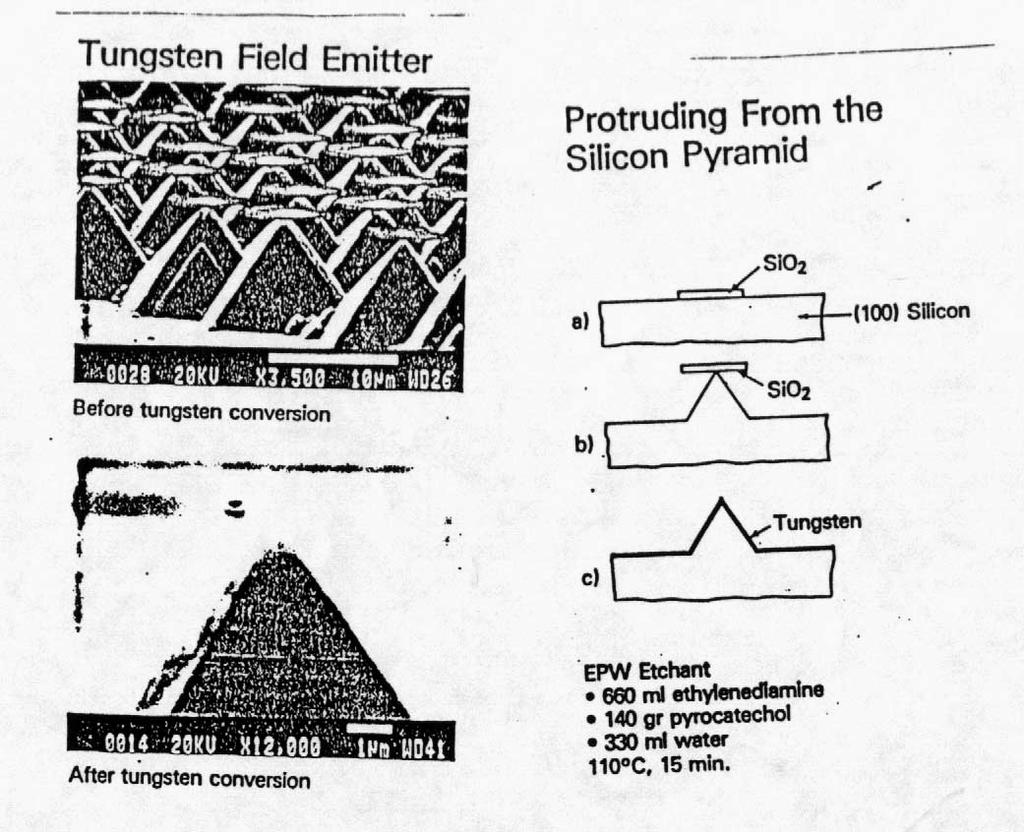
24 (3) Field-Emission Tips 24
25 Drawbacks o Wet Etching Lack o anisotropy Poor process control Excessie particulate contamination => Wet etching used or noncritical eature sizes 25
Section 3: Etching. Jaeger Chapter 2 Reader
 Section 3: Etching Jaeger Chapter 2 Reader Etch rate Etch Process - Figures of Merit Etch rate uniformity Selectivity Anisotropy d m Bias and anisotropy etching mask h f substrate d f d m substrate d f
4FNJDPOEVDUPS 'BCSJDBUJPO &UDI
 2010.5.4 1 Major Fabrication Steps in CMOS Process Flow UV light oxygen Silicon dioxide Silicon substrate Oxidation (Field oxide) photoresist Photoresist Coating Mask exposed photoresist Mask-Wafer Exposed
Lecture 11. Etching Techniques Reading: Chapter 11. ECE Dr. Alan Doolittle
 Lecture 11 Etching Techniques Reading: Chapter 11 Etching Techniques Characterized by: 1.) Etch rate (A/minute) 2.) Selectivity: S=etch rate material 1 / etch rate material 2 is said to have a selectivity
Lecture 15 Etching. Chapters 15 & 16 Wolf and Tauber. ECE611 / CHE611 Electronic Materials Processing Fall John Labram 1/76
 Lecture 15 Etching Chapters 15 & 16 Wolf and Tauber 1/76 Announcements Term Paper: You are expected to produce a 4-5 page term paper on a selected topic (from a list). Term paper contributes 25% of course
Reactive Ion Etching (RIE)
") Reactive Ion Etching (RIE) RF 13.56 ~ MHz plasma Parallel-Plate Reactor wafers Sputtering Plasma generates (1) Ions (2) Activated neutrals Enhance chemical reaction 1 2 Remote Plasma Reactors Plasma Sources
Reactive Ion Etching (RIE) RF 13.56 ~ MHz plasma Parallel-Plate Reactor wafers Sputtering Plasma generates (1) Ions (2) Activated neutrals Enhance chemical reaction 1 2 Remote Plasma Reactors Plasma Sources
CHAPTER 6: Etching. Chapter 6 1
 Chapter 6 1 CHAPTER 6: Etching Different etching processes are selected depending upon the particular material to be removed. As shown in Figure 6.1, wet chemical processes result in isotropic etching
ETCHING Chapter 10. Mask. Photoresist
 ETCHING Chapter 10 Mask Light Deposited Substrate Photoresist Etch mask deposition Photoresist application Exposure Development Etching Resist removal Etching of thin films and sometimes the silicon substrate
Etching: Basic Terminology
 Lecture 7 Etching Etching: Basic Terminology Introduction : Etching of thin films and sometimes the silicon substrate are very common process steps. Usually selectivity, and directionality are the first
Etching terminology. d mask. h film. film substrate. d film. bias B. anisotropy A. etch mask. B d f - d m (i.e., twice the undercut) A film
 A film") Etching terminology h ilm d mask etch mask ilm substrate d mask bias B B d - d m (i.e., twice the undercut) anisotropy A d ilm d ilm A ilm 1 - v l / v v v l lateral etch rate v v vertical etch rate or
Etching terminology h ilm d mask etch mask ilm substrate d mask bias B B d - d m (i.e., twice the undercut) anisotropy A d ilm d ilm A ilm 1 - v l / v v v l lateral etch rate v v vertical etch rate or
Device Fabrication: Etch
 Device Fabrication: Etch 1 Objectives Upon finishing this course, you should able to: Familiar with etch terminology Compare wet and dry etch processes processing and list the main dry etch etchants Become
UNIT 3. By: Ajay Kumar Gautam Asst. Prof. Dev Bhoomi Institute of Technology & Engineering, Dehradun
 UNIT 3 By: Ajay Kumar Gautam Asst. Prof. Dev Bhoomi Institute of Technology & Engineering, Dehradun 1 Syllabus Lithography: photolithography and pattern transfer, Optical and non optical lithography, electron,
課程名稱 : 微製造技術 Microfabrication Technology. 授課教師 : 王東安 Lecture 6 Etching
 課程名稱 : 微製造技術 Microfabrication Technology 授課教師 : 王東安 Lecture 6 Etching 1 Lecture Outline Reading Campbell: Chapter 11 Today s lecture Wet etching Chemical mechanical polishing Plasma etching Ion milling
Lithography and Etching
 Lithography and Etching Victor Ovchinnikov Chapters 8.1, 8.4, 9, 11 Previous lecture Microdevices Main processes: Thin film deposition Patterning (lithography) Doping Materials: Single crystal (monocrystal)
Wet and Dry Etching. Theory
 Wet and Dry Etching Theory 1. Introduction Etching techniques are commonly used in the fabrication processes of semiconductor devices to remove selected layers for the purposes of pattern transfer, wafer
EE 527 MICROFABRICATION. Lecture 24 Tai-Chang Chen University of Washington
 EE 527 MICROFABRICATION Lecture 24 Tai-Chang Chen University of Washington EDP ETCHING OF SILICON - 1 Ethylene Diamine Pyrocatechol Anisotropy: (100):(111) ~ 35:1 EDP is very corrosive, very carcinogenic,
EE 527 MICROFABRICATION. Lecture 25 Tai-Chang Chen University of Washington
 EE 527 MICROFABRICATION Lecture 25 Tai-Chang Chen University of Washington ION MILLING SYSTEM Kaufmann source Use e-beam to strike plasma A magnetic field applied to increase ion density Drawback Low etch
E SC 412 Nanotechnology: Materials, Infrastructure, and Safety Wook Jun Nam
 E SC 412 Nanotechnology: Materials, Infrastructure, and Safety Wook Jun Nam Lecture 10 Outline 1. Wet Etching/Vapor Phase Etching 2. Dry Etching DC/RF Plasma Plasma Reactors Materials/Gases Etching Parameters
LECTURE 5 SUMMARY OF KEY IDEAS
 LECTURE 5 SUMMARY OF KEY IDEAS Etching is a processing step following lithography: it transfers a circuit image from the photoresist to materials form which devices are made or to hard masking or sacrificial
Dry Etching Zheng Yang ERF 3017, MW 5:15-6:00 pm
 Dry Etching Zheng Yang ERF 3017, email: yangzhen@uic.edu, MW 5:15-6:00 pm Page 1 Page 2 Dry Etching Why dry etching? - WE is limited to pattern sizes above 3mm - WE is isotropic causing underetching -
EE C245 ME C218 Introduction to MEMS Design
 EE C245 ME C218 Introduction to MEMS Design Fall 2008 Prof. Clark T.-C. Nguyen Dept. of Electrical Engineering & Computer Sciences University of California at Berkeley Berkeley, CA 94720 Lecture 6: Process
Outline. 1 Introduction. 2 Basic IC fabrication processes. 3 Fabrication techniques for MEMS. 4 Applications. 5 Mechanics issues on MEMS 1 MDL NTHU
 Outline 1 Introduction 2 Basic IC fabrication processes 3 Fabrication techniques for MEMS 4 Applications 5 Mechanics issues on MEMS 1 MDL 2. Basic IC fabrication processes 2.1 Deposition and growth 2.2
UNIVERSITY OF CALIFORNIA College of Engineering Department of Electrical Engineering and Computer Sciences. Fall Exam 1
 UNIVERSITY OF CALIFORNIA College of Engineering Department of Electrical Engineering and Computer Sciences EECS 143 Fall 2008 Exam 1 Professor Ali Javey Answer Key Name: SID: 1337 Closed book. One sheet
Lecture 6 Plasmas. Chapters 10 &16 Wolf and Tauber. ECE611 / CHE611 Electronic Materials Processing Fall John Labram 1/68
 Lecture 6 Plasmas Chapters 10 &16 Wolf and Tauber 1/68 Announcements Homework: Homework will be returned to you on Thursday (12 th October). Solutions will be also posted online on Thursday (12 th October)
EE C247B / ME C218 INTRODUCTION TO MEMS DESIGN SPRING 2016 C. NGUYEN PROBLEM SET #4
 Issued: Wednesday, March 4, 2016 PROBLEM SET #4 Due: Monday, March 14, 2016, 8:00 a.m. in the EE C247B homework box near 125 Cory. 1. This problem considers bending of a simple cantilever and several methods
CVD: General considerations.
 CVD: General considerations. PVD: Move material from bulk to thin film form. Limited primarily to metals or simple materials. Limited by thermal stability/vapor pressure considerations. Typically requires
3.155J/6.152J Microelectronic Processing Technology Fall Term, 2004
 3.155J/6.152J Microelectronic Processing Technology Fall Term, 2004 Bob O'Handley Martin Schmidt Quiz Nov. 17, 2004 Ion implantation, diffusion [15] 1. a) Two identical p-type Si wafers (N a = 10 17 cm
Etching Issues - Anisotropy. Dry Etching. Dry Etching Overview. Etching Issues - Selectivity
 Etching Issues - Anisotropy Dry Etching Dr. Bruce K. Gale Fundamentals of Micromachining BIOEN 6421 EL EN 5221 and 6221 ME EN 5960 and 6960 Isotropic etchants etch at the same rate in every direction mask
Chapter 9, Etch. Hong Xiao, Ph. D. www2.austin.cc.tx.us/hongxiao/book.htm
 Chapter 9, Etch Hong Xiao, Ph. D. hxiao89@hotmail.com www2.austin.cc.tx.us/hongxiao/book.htm Hong Xiao, Ph. D. www2.austin.cc.tx.us/hongxiao/book.htm 1 Objectives Upon finishing this course, you should
EE C245 ME C218 Introduction to MEMS Design Fall 2010
 Lecture Outline EE C245 ME C28 Introduction to MEMS Design Fall 200 Prof. Clark T.-C. Nguyen Dept. of Electrical Engineering & Computer Sciences University of California at Berkeley Berkeley, CA 94720
Lecture 150 Basic IC Processes (10/10/01) Page ECE Analog Integrated Circuits and Systems P.E. Allen
 Page ECE Analog Integrated Circuits and Systems P.E. Allen") Lecture 150 Basic IC Processes (10/10/01) Page 1501 LECTURE 150 BASIC IC PROCESSES (READING: TextSec. 2.2) INTRODUCTION Objective The objective of this presentation is: 1.) Introduce the fabrication of
Lecture 150 Basic IC Processes (10/10/01) Page 1501 LECTURE 150 BASIC IC PROCESSES (READING: TextSec. 2.2) INTRODUCTION Objective The objective of this presentation is: 1.) Introduce the fabrication of
 Institute of Physics Publishing Journal of Physics: Conference Series 34 (2006) 1038 1043 doi:10.1088/1742-6596/34/1/172 International MEMS Conference 2006 Characterisation of anisotropic etching in KOH
ELEC 7364 Lecture Notes Summer Etching. by STELLA W. PANG. from The University of Michigan, Ann Arbor, MI, USA
 ELEC 7364 Lecture Notes Summer 2008 Etching by STELLA W. PANG from The University of Michigan, Ann Arbor, MI, USA Visiting Professor at The University of Hong Kong The University of Michigan on Visiting
EE 143 MICROFABRICATION TECHNOLOGY FALL 2014 C. Nguyen PROBLEM SET #7. Due: Friday, Oct. 24, 2014, 8:00 a.m. in the EE 143 homework box near 140 Cory
 Issued: Tuesday, Oct. 14, 2014 PROBLEM SET #7 Due: Friday, Oct. 24, 2014, 8:00 a.m. in the EE 143 homework box near 140 Cory Electroplating 1. Suppose you want to fabricate MEMS clamped-clamped beam structures
The Stanford Nanofabrication Facility. Etch Area Overview. May 21, 2013
 The Stanford Nanofabrication Facility Etch Area Overview May 21, 2013 High Density Plasma Systems Etcher Materials Etched Gases available Wafer Size Applied Materials P5000 MRIE ChA Applied Materials P5000
EE C245 ME C218 Introduction to MEMS Design Fall 2007
 EE C245 ME C218 Introduction to MEMS Design Fall 2007 Prof. Clark T.-C. Nguyen Dept. of Electrical Engineering & Computer Sciences University of California at Berkeley Berkeley, CA 94720 Lecture 11: Bulk
Regents of the University of California
 Deep Reactive-Ion Etching (DRIE) DRIE Issues: Etch Rate Variance The Bosch process: Inductively-coupled plasma Etch Rate: 1.5-4 μm/min Two main cycles in the etch: Etch cycle (5-15 s): SF 6 (SF x+ ) etches
EE C245 ME C218 Introduction to MEMS Design Fall 2007
 EE C245 ME C218 Introduction to MEMS Design Fall 2007 Prof. Clark T.-C. Nguyen Dept. of Electrical Engineering & Computer Sciences University of California at Berkeley Berkeley, CA 94720 Lecture 12: Mechanics
26. N 2 + H 2 NH N 2 + O 2 N 2 O 28. CO 2 + H 2 O C 6 H 12 O 6 + O SiCl 4 + H 2 O H 4 SiO 4 + HCl 30. H 3 PO 4 H 4 P 2 O 7 + H 2 O
 Balance the following chemical equations: (Some may already be balanced.) 1. H 2 + O 2 H 2 O 2. S 8 + O 2 SO 3 3. HgO Hg + O 2 4. Zn + HCl ZnCl 2 + H 2 5. Na + H 2 O NaOH + H 2 6. C 10 H 16 + Cl 2 C +
1. Narrative Overview Questions
 Homework 4 Due Nov. 16, 010 Required Reading: Text and Lecture Slides on Downloadable from Course WEB site: http://courses.washington.edu/overney/nme498.html 1. Narrative Overview Questions Question 1
MICROCHIP MANUFACTURING by S. Wolf
 by S. Wolf Chapter 5: GASES, LIQUID-CHEMICALS, & ULTRAPURE-WATER FOR ULSI Chapter 5: Gases, Liquid-Chemicals & CHAPTER CONTENTS Basic Properties of Materials Temperature Thermal Expasio of Materials Liquid
UNIVERSITY OF CALIFORNIA. College of Engineering. Department of Electrical Engineering and Computer Sciences. Professor Ali Javey.
 UNIVERSITY OF CALIFORNIA College of Engineering Department of Electrical Engineering and Computer Sciences EE 143 Professor Ali Javey Spring 2009 Exam 2 Name: SID: Closed book. One sheet of notes is allowed.
AP Chemistry - Summer Assignment
 AP Chemistry - Summer Assignment NOTE: a. MUST SHOW ALL WORK FOR CREDIT!! b. Where work is required, do on a separate sheet of paper c. These are the foundational things you should be able to do when you
Film Deposition Part 1
 1 Film Deposition Part 1 Chapter 11 : Semiconductor Manufacturing Technology by M. Quirk & J. Serda Spring Semester 2013 Saroj Kumar Patra Semidonductor Manufacturing Technology, Norwegian University of
DQN Positive Photoresist
 UNIVESITY OF CALIFONIA, BEKELEY BEKELEY DAVIS IVINE LOS ANGELES IVESIDE SAN DIEGO SAN FANCISCO SANTA BABAA SANTA CUZ DEPATMENT OF BIOENGINEEING 94720-1762 BioE 121 Midterm #1 Solutions BEKELEY, CALIFONIA
EE143 LAB. Professor N Cheung, U.C. Berkeley
 EE143 LAB 1 1 EE143 Equipment in Cory 218 2 Guidelines for Process Integration * A sequence of Additive and Subtractive steps with lateral patterning Processing Steps Si wafer Watch out for materials compatibility
Plasma etch control by means of physical plasma parameter measurement with HERCULES Sematech AEC/APC Symposium X
 Plasma etch control by means of physical plasma parameter measurement with HERCULES A. Steinbach F. Bell D. Knobloch S. Wurm Ch. Koelbl D. Köhler -1- Contents - Introduction - Motivation - Plasma monitoring
C. Incorrect! These are the correct symbols, but the charges must be balanced. D. Correct! The charges are balanced in this formula.
 SAT Chemistry - Problem Drill 07: Writing Chemical Formulas No. 1 of 10 1. Which of the following is correct for sodium oxide? (A) SO (B) S 2 O (C) NaO (D) Na 2 O (E) NaO 2 Sodium is symbolized with Na.
SILICON DIOXIDE TO POLYSILICON SELECTIVITY OF A C2F6/CHF3 DRY ETCH PROCESS
 SLCON DOXDE TO POLYSLCON SELECTVTY OF A C2F6/CHF3 DRY ETCH PROCESS Craig L. Kuhi 5th Year Microelectronic Engineering Student Rochester nstitute of Technology ABSTRACT The etch rates and selectivity of
Acid/Base Definitions
 Acids and Bases Acid/Base Definitions Arrhenius Model Acids produce hydrogen ions in aqueous solutions Bases produce hydroxide ions in aqueous solutions Bronsted-Lowry Model Acids are proton donors Bases
EE-612: Lecture 22: CMOS Process Steps
 EE-612: Lecture 22: CMOS Process Steps Mark Lundstrom Electrical and Computer Engineering Purdue University West Lafayette, IN USA Fall 2006 NCN www.nanohub.org Lundstrom EE-612 F06 1 outline 1) Unit Process
Chemical Equations. Shorthand way of describing a chemical change or reaction. Reactants Products
 Chemical Equations Shorthand way of describing a chemical change or reaction. Reactants Products All chemical equations MUST be balanced: 1. Material balance - # atoms of each element must be the same
Particle Relative Mass Charge
 ADVANCED CHEMISTRY REVISION THE FIRST 5 WEEKS 1. Define each of the following words so that you can differentiate between them:- ELEMENT and COMPOUND, ATOM and MOLECULE An element is comprised of one type
EE C245 ME C218 Introduction to MEMS Design Fall 2007
 EE C245 ME C218 Introduction to MEMS Design Fall 2007 Prof. Clark T.-C. Nguyen Dept. of Electrical Engineering & Computer Sciences University of California at Berkeley Berkeley, CA 94720 Lecture 4: Film
Nanofabrication of direct positioning atomic force microscope (AFM) probes and a novel method to attain controllable lift-off
 probes and a novel method to attain controllable lift-off") Nanofabrication of direct positioning atomic force microscope (AFM) probes and a novel method to attain controllable lift-off by Shuo Zheng A thesis presented to University of Waterloo in the fulfillment
Nanofabrication of direct positioning atomic force microscope (AFM) probes and a novel method to attain controllable lift-off by Shuo Zheng A thesis presented to University of Waterloo in the fulfillment
Section 1 Introduction to Stoichiometry. Describe the importance of the mole ratio in stoichiometric calculations.
 Section 1 Introduction to Stoichiometry Objective Define stoichiometry. Describe the importance of the mole ratio in stoichiometric calculations. Write a mole ratio relating two substances in a chemical
2.76/2.760 Multiscale Systems Design & Manufacturing
 2.76/2.760 Multiscale Systems Design & Manufacturing Fall 2004 MOEMS Devices for Optical communications system Switches and micromirror for Add/drops Diagrams removed for copyright reasons. MOEMS MEMS
Supplementary Information Our InGaN/GaN multiple quantum wells (MQWs) based one-dimensional (1D) grating structures
 based one-dimensional (1D) grating structures") Polarized white light from hybrid organic/iii-nitrides grating structures M. Athanasiou, R. M. Smith, S. Ghataora and T. Wang* Department of Electronic and Electrical Engineering, University of Sheffield,
Polarized white light from hybrid organic/iii-nitrides grating structures M. Athanasiou, R. M. Smith, S. Ghataora and T. Wang* Department of Electronic and Electrical Engineering, University of Sheffield,
NNCI ETCH WORKSHOP - STANFORD NNCI PLASMA ETCH OVERVIEW. Usha Raghuram Stanford Nanofabrication Facility Stanford, CA May 24, 2016
 NNCI ETCH WORKSHOP - STANFORD NNCI PLASMA ETCH OVERVIEW Usha Raghuram Stanford Nanofabrication Facility Stanford, CA May 24, 2016 NNCI AT STANFORD Four labs under NNCI Umbrella at Stanford SNSF Stanford
Plasma Deposition (Overview) Lecture 1
 Lecture 1") Plasma Deposition (Overview) Lecture 1 Material Processes Plasma Processing Plasma-assisted Deposition Implantation Surface Modification Development of Plasma-based processing Microelectronics needs (fabrication
Plasma Deposition (Overview) Lecture 1 Material Processes Plasma Processing Plasma-assisted Deposition Implantation Surface Modification Development of Plasma-based processing Microelectronics needs (fabrication
Inorganic Nomenclature
 Inorganic Nomenclature A. The Chemical Elements 1. The term INORGANIC NOMENCLATURE refers to the naming of elements and inorganic compounds. Recall that ELEMENTS are the simplest form of matter that cannot
Chapter 7 ACIDS AND BASES. Exercises
 Chapter 7 ACIDS AND BASES Exercises 7.2 (a) A nonpolar solvent because phosphorus pentachloride is a nonpolar covalent compound. (b) A polar protic solvent because cesium chloride is ionic. Ionic compounds
MASSACHUSETTS INSTITUTE OF TECHNOLOGY DEPARTMENT OF MATERIALS SCIENCE AND ENGINEERING CAMBRIDGE, MASSACHUSETTS 02139
 MASSACHUSTTS INSTITUT OF TCHNOLOGY DPARTMNT OF MATRIALS SCINC AND NGINRING CAMBRIDG, MASSACHUSTTS 0239 322 MCHANICAL PROPRTIS OF MATRIALS PROBLM ST 4 SOLUTIONS Consider a 500 nm thick aluminum ilm on a
IC Fabrication Technology
 IC Fabrication Technology * History: 1958-59: J. Kilby, Texas Instruments and R. Noyce, Fairchild * Key Idea: batch fabrication of electronic circuits n entire circuit, say 10 7 transistors and 5 levels
Copyright Warning & Restrictions
 Copyright Warning & Restrictions The copyright law of the United States (Title 17, United States Code) governs the making of photocopies or other reproductions of copyrighted material. Under certain conditions
Aqueous Equilibria, Part 1 AP Chemistry Lecture Outline
 Aqueous Equilibria, Part 1 AP Chemistry Lecture Outline Name: Acids and Bases Arrhenius...acids increase the when dissolved in H 2 O....bases increase the when dissolved in H 2 O. e.g., HCl and NaOH Bronsted-Lowry
Chapter 7 Acids and Bases
 Chapter 7 Acids and Bases 7.1 The Nature of Acids and Bases 7.2 Acid Strength 7.3 The ph Scale 7.4 Calculating the ph of Strong Acid Solutions 7.5 Calculating the ph of Weak Acid Solutions 7.6 Bases 7.7
Self-study problems and questions Processing and Device Technology, FFF110/FYSD13
 Self-study problems and questions Processing and Device Technology, FFF110/FYSD13 Version 2016_01 In addition to the problems discussed at the seminars and at the lectures, you can use this set of problems
Plasma etching. Bibliography
 Plasma etching Bibliography 1. B. Chapman, Glow discharge processes, (Wiley, New York, 1980). - Classical plasma processing of etching and sputtering 2. D. M. Manos and D. L. Flamm, Plasma etching; An
Chemical Formulas & Chemical Compounds. Chemical formula indicates the relative number of atoms of each kind in a chemical compound.
 Unit 6: Chemical Formulas & Chemical Compounds Chemical Names & Formulas Chemical formula indicates the relative number of atoms of each kind in a chemical compound. Molecular compound - it s formula reveals
Chapter 4; Reactions in Aqueous Solutions. Chapter 4; Reactions in Aqueous Solutions. V. Molarity VI. Acid-Base Titrations VII. Dilution of Solutions
 Chapter 4; Reactions in Aqueous Solutions I. Electrolytes vs. NonElectrolytes II. Precipitation Reaction a) Solubility Rules III. Reactions of Acids a) Neutralization b) Acid and Carbonate c) Acid and
Characterization of Post-etch Residue Clean By Chemical Bonding Transformation Mapping
 Characterization of Post-etch Residue Clean By Chemical Bonding Transformation Mapping Muthappan Asokan, Oliver Chyan*, Interfacial Electrochemistry and Materials Research Lab, University of North Texas
2H 2 (g) + O 2 (g) 2H 2 O (g)
 + O 2 (g) 2H 2 O (g)") Mass A AP Chemistry Stoichiometry Review Pages Mass to Mass Stoichiometry Problem (Review) Moles A Moles B Mass B Mass of given Amount of given Amount of unknown Mass of unknown in grams in Moles in moles
Mass A AP Chemistry Stoichiometry Review Pages Mass to Mass Stoichiometry Problem (Review) Moles A Moles B Mass B Mass of given Amount of given Amount of unknown Mass of unknown in grams in Moles in moles
Chapter (3) Motion. in One. Dimension
 Motion. in One. Dimension") Chapter (3) Motion in One Dimension Pro. Mohammad Abu Abdeen Dr. Galal Ramzy Chapter (3) Motion in one Dimension We begin our study o mechanics by studying the motion o an object (which is assumed to be
Chapter (3) Motion in One Dimension Pro. Mohammad Abu Abdeen Dr. Galal Ramzy Chapter (3) Motion in one Dimension We begin our study o mechanics by studying the motion o an object (which is assumed to be
Thin Film Transistors (TFT)
") Thin Film Transistors (TFT) a-si TFT - α-si:h (Hydrogenated amorphous Si) deposited with a PECVD system (low temp. process) replaces the single crystal Si substrate. - Inverted staggered structure with
Thin Film Transistors (TFT) a-si TFT - α-si:h (Hydrogenated amorphous Si) deposited with a PECVD system (low temp. process) replaces the single crystal Si substrate. - Inverted staggered structure with
DO NOT WRITE YOUR NAME OR KAUST ID NUMBER ON THIS PAGE OR ANY OTHER PAGE PUT YOUR EXAM ID NUMBER ON THIS PAGE AND EVERY OTHER PAGE YOU SUBMIT
 DO NOT WRITE YOUR NAME OR KAUST ID NUMBER ON THIS PAGE OR ANY OTHER PAGE PUT YOUR EXAM ID NUMBER ON THIS PAGE AND EVERY OTHER PAGE YOU SUBMIT WRITE YOUR SOLUTIONS ON ONLY ONE SIDE OF EMPTY SOLUTION SHEETS
Funsheet 9.1 [VSEPR] Gu 2015
![Funsheet 9.1 [VSEPR] Gu 2015](/thumbs/95/122549630.jpg "Funsheet 9.1 [VSEPR] Gu 2015") Funsheet 9.1 [VSEPR] Gu 2015 Molecule Lewis Structure # Atoms Bonded to Central Atom # Lone Pairs on Central Atom Name of Shape 3D Lewis Structure NI 3 CF 4 OCl 2 C 2 F 2 HOF Funsheet 9.1 [VSEPR] Gu 2015
Funsheet 9.1 [VSEPR] Gu 2015 Molecule Lewis Structure # Atoms Bonded to Central Atom # Lone Pairs on Central Atom Name of Shape 3D Lewis Structure NI 3 CF 4 OCl 2 C 2 F 2 HOF Funsheet 9.1 [VSEPR] Gu 2015
I. Properties of Aqueous Solutions A) Electrolytes and Non-Electrolytes B) Predicting Solubility* II. Reactions of Ionic Compounds in Solution*
 Electrolytes and Non-Electrolytes B) Predicting Solubility* II. Reactions of Ionic Compounds in Solution*") Chapter 5 Reactions in Aqueous Solutions Titrations Kick Acid!!! 1 I. Properties of Aqueous Solutions A) Electrolytes and Non-Electrolytes B) Predicting Solubility* II. Reactions of Ionic Compounds in
Chapter 5 Reactions in Aqueous Solutions Titrations Kick Acid!!! 1 I. Properties of Aqueous Solutions A) Electrolytes and Non-Electrolytes B) Predicting Solubility* II. Reactions of Ionic Compounds in
Introduction to Photolithography
 http://www.ichaus.de/news/72 Introduction to Photolithography Photolithography The following slides present an outline of the process by which integrated circuits are made, of which photolithography is
Unit 4-1 Provincial Practice Questions Page 1
 Page 1 Page 2 Page 3 Page 4 Page 5 1.00 Page 6 Page 7 Page 8 55. The conjugate base of HAsO 4 2 is A. H 3 O + B. 3 AsO 4 C. H 3 AsO 4 D. H 2 AsO 4 56. Consider the following acidbase equilibrium: HC 6
Stoichiometry: Calculations with Chemical Formulas and Equations (Chapter 3) Past Quiz and Test Questions
 Past Quiz and Test Questions") Stoichiometry: Calculations with Chemical Formulas and Equations (Chapter 3) Past Quiz and Test Questions 1. Balance the following equations Al 2 (SO 4 ) 3 (aq) + Ba(NO 3 ) 2 (aq) ----> Al(NO 3 ) 3 (aq)
Stoichiometry: Calculations with Chemical Formulas and Equations (Chapter 3) Past Quiz and Test Questions 1. Balance the following equations Al 2 (SO 4 ) 3 (aq) + Ba(NO 3 ) 2 (aq) ----> Al(NO 3 ) 3 (aq)
Chapter 9 Stoichiometry
 Chapter 9 Stoichiometry Section 9.1 Intro to Stoichiometry 9.1 Objectives Define stoichiometry. Describe the importance of the mole ratio in stoichiometric calculations. Write a mole ratio relating two
A. Optimizing the growth conditions of large-scale graphene films
 1 A. Optimizing the growth conditions of large-scale graphene films Figure S1. Optical microscope images of graphene films transferred on 300 nm SiO 2 /Si substrates. a, Images of the graphene films grown
FLUID MECHANICS. Lecture 7 Exact solutions
 FLID MECHANICS Lecture 7 Eact solutions 1 Scope o Lecture To present solutions or a ew representative laminar boundary layers where the boundary conditions enable eact analytical solutions to be obtained.
Chapter 11 Collision Theory
 Chapter Collision Theory Introduction. Center o Mass Reerence Frame Consider two particles o masses m and m interacting ia some orce. Figure. Center o Mass o a system o two interacting particles Choose
Chapter 9. Preview. Lesson Starter Objective Stoichiometry Definition Reaction Stoichiometry Problems Mole Ratio Stoichiometry Calculations
 Preview Lesson Starter Objective Stoichiometry Definition Reaction Stoichiometry Problems Mole Ratio Stoichiometry Section 1 Introduction to Stoichiometry Lesson Starter Mg(s) + 2HCl(aq) MgCl 2 (aq) +
Inorganic Nomenclature
 Inorganic Nomenclature http://www.msu.edu/user/dynicrai/physics/h2o.htm A. The Chemical Elements 1. The term INORGANIC NOMENCLATURE refers to the naming of elements and inorganic compounds. Recall that
Chapter 2: Review of Microbolometer
 Chapter 2: Review of Microbolometer In this chapter, the basics of microbolometer theory and micromachining are covered. The theory of microbolometer detectors is discussed in detail, as well as their
CHM 1046 Test #4 April 24, 2001
 CHM 1046 Test #4 April 24, 2001 1. Which one of the following is a strong acid? a. H 2 CO 3 b. H 2 SO 3 c. H 2 SO 4 d. H 3 PO 4 e. CH 3 COOH 2. The substance (CH 3 CH 2 ) 2 NH is considered a. a weak acid
Name: Date: M O L A R M A S S & P E R C E N T C O M P O S I T I O N
 Name: Date: M O L A R M A S S & P E R C E N T C O M P O S I T I O N I. Molar Masses Given a periodic table, you should be able to calculate the molecular mass (in amu s) or the molar mass (in grams) for
The Major Classes of Chemical Reactions
 Chapter 4 The Major Classes of Chemical Reactions 5.1 Properties of compounds in Aqueous Solution 5.2 Precipitation Reaction 5.3 Acids and Bases 5.4 Reactions of Acid and Bases 5.5 Gas-forming Reactions
Chapter 3: Acid Base Equilibria. HCl + KOH KCl + H 2 O acid + base salt + water
 Chapter 3: Acid Base Equilibria HCl + KOH KCl + H 2 O acid + base salt + water What is an acid? The Arrhenius concept proposed that acids are substances that produce hydrogen ions (H + ) in aqueous solutions.
In-situ Monitoring of Thin-Film Formation Processes by Spectroscopic Ellipsometry
 In-situ Monitoring of Thin-Film Formation Processes by Spectroscopic Ellipsometry Alexey Kovalgin Chair of Semiconductor Components MESA+ Institute for Nanotechnology Motivation Advantages of in-situ over
Chapter 7 Plasma Basic
 Chapter 7 Plasma Basic Hong Xiao, Ph. D. hxiao89@hotmail.com www2.austin.cc.tx.us/hongxiao/book.htm Hong Xiao, Ph. D. www2.austin.cc.tx.us/hongxiao/book.htm 1 Objectives List at least three IC processes
Chapter 7: Stoichiometry in Chemical Reactions
 Chapter 7: Stoichiometry in Chemical Reactions Mini Investigation: Precipitating Ratios, page 315 A. ZnCl 2 (aq) + Na 2 CO 3 (aq) ZnCO 3 (s) + 2 NaCl(aq) 3 AgNO 3 (aq) + Na 3 PO 4 (aq) Ag 3 PO 4 (s) +
Characteristics of Neutral Beam Generated by a Low Angle Reflection and Its Etch Characteristics by Halogen-Based Gases
 Characteristics of Neutral Beam Generated by a Low Angle Reflection and Its Etch Characteristics by Halogen-Based Gases Geun-Young Yeom SungKyunKwan University Problems of Current Etch Technology Scaling
BCB WAFER BONDING COMPATIBLE WITH BULK MICRO MACHINING TAE-JOO HWANG
 Proceedings of IPACK03 International Electronic Packaging Technical Conference and Exhibition July 6 11, 2003, Maui, Hawaii, USA InterPack2003-35011 WAFER BONDING COMPATIBLE WITH BULK MICRO MACHINING TAE-JOO
Free-Space MEMS Tunable Optical Filter in (110) Silicon
 Silicon") Free-Space MEMS Tunable Optical Filter in (110) Silicon Ariel Lipson & Eric M. Yeatman Optical & Semiconductor Group Outline Device - Optical Filter Optical analysis Fabrication Schematic Fabricated 2
Free-Space MEMS Tunable Optical Filter in (110) Silicon Ariel Lipson & Eric M. Yeatman Optical & Semiconductor Group Outline Device - Optical Filter Optical analysis Fabrication Schematic Fabricated 2
ACID-BASE REACTIONS & THE ph SCALE
 Introduction ACID-BASE REACTIONS & THE ph SCALE In acid-base reactions in aqueous solution, the active agents are commonly the hydronium ion H 3 0 + or the hydroxide ion OH. The range of concentrations
Acids and Bases. Reading Assignments: Acids. Bases. Chapter 15 in R. Chang, Chemistry, 8th Ed., McGraw-Hill, 2005
 Reading Assignments: Chapter 15 in R. Chang, Chemistry, 8th Ed., McGraw-Hill, 2005 Or Related topics in other textbooks. Acids and Bases Consultation outside lecture room: Office Hours: Tuesday & Thursday
Chapter 14. Objectives
 Section 1 Properties of Acids and Bases Objectives List five general properties of aqueous acids and bases. Name common binary acids and oxyacids, given their chemical formulas. List five acids commonly