Stop Watch (System Controller Approach)
|
|
|
- Cathleen Hunt
- 5 years ago
- Views:
Transcription
1 Stop Watch (System Controller Approach)
2 Problem Design a stop watch that can measure times taken for two events Inputs CLK = 6 Hz RESET: Asynchronously reset everything X: comes from push button First Push: Start timer Second Push: Store the time taken for the first event Third Push: Store the time taken for the second event SEL: select output (High: first event time, Low: second event time) Outputs Two decimal digits to be connected to two seven segment displays Can display ~ 99
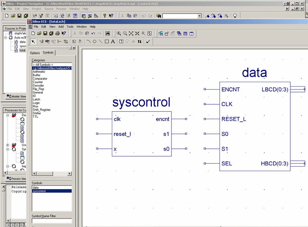
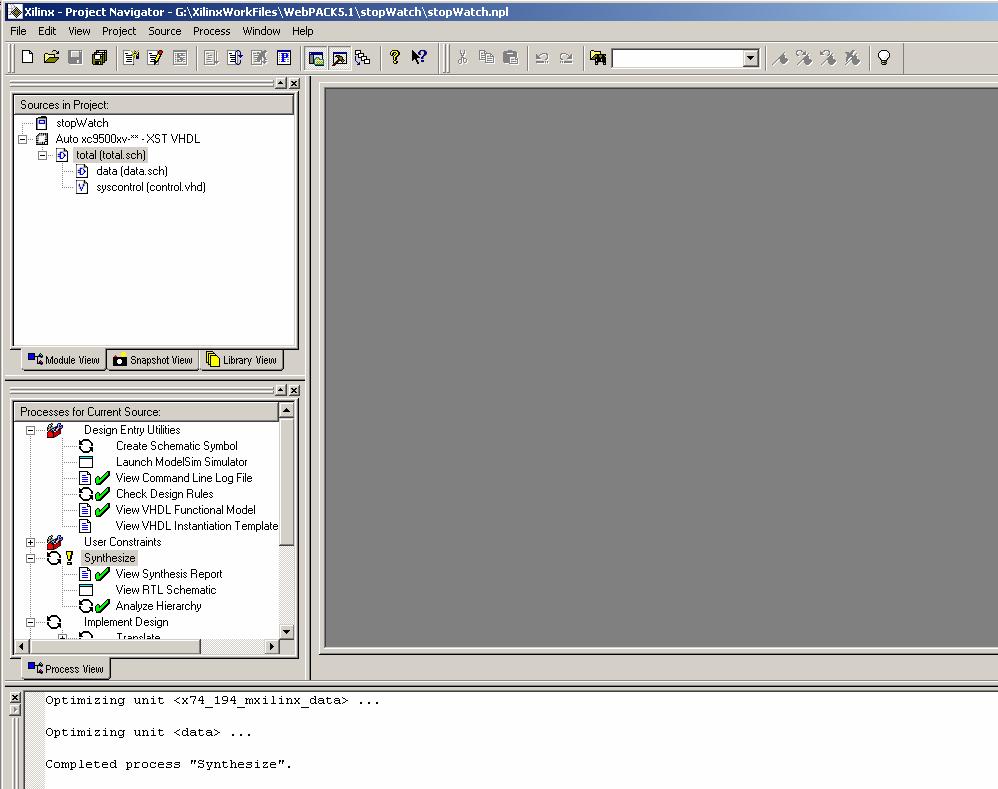
3 Overall Architecture Design CLK TENSEC SEC RESET X SEL Which LBB (among those we learn in the class) and how many? How to decompose the whole system into data part and control part?
4 Design System Architecture First step: divide the system into a control unit and data unit Data unit stores, routes, combines, and generally process data Control unit starting & stopping the process, testing conditions, and deciding what to do next
5
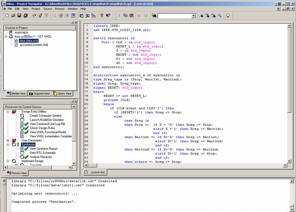
6 System controller design
7 Table (Variable Entered Table) P.S. N.S. Output State symbol Q Q D D S S ENCNT A B C unused
8 Excitation Eqs, Output Eqs Q Q D= D= Q Q Q S= S= ENCNT=
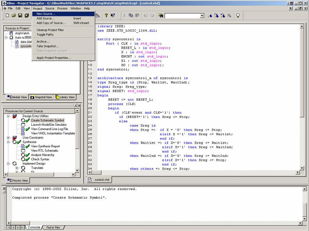
9 Alternative (VHDL program)
10
11
12
13
14
15 4-bit Serial Adder (Decomposing state machines, synchronous design methodology, system controller design)
16 Review of combinational adders -bit full adder and 4-bit ripple adder
17 Binary serial adder Serial input feed (two data streams A and B) Generate serial output CLR clear the previous carry synchronously A i CLR HOLD S i HOLD hold the previous value of the carry B i Carry
18 Binary serial adder implementation LS83: dual bit full adders carry A B Q(Carry) S
19 Problem Statement Design a 4-bit adder based on a serial approach Parallel feed of X and X2 Parallel out of Y comes out after few cycles Final carry available X X START may be long (External guy will negate START only after detecting DONE) START CONTROL 4-bit adder 4 DONE if CONTROL=, X plus X 2 Y if CONTROL=, X plus Y Y CARRY Y
20 Start from LBB Here, we have some basic building blocks in mind 4-bit shift registers, binary serial adder, etc Tie these elements together and make them controllable from the outside world We want to take maximum advantage of common building blocks (MSI chips that are available)
21 Design System Architecture First step: divide the system into a control unit and data unit Data unit stores, routes, combines, and generally process data Control unit starting & stopping the process, testing conditions, and deciding what to do next
22 Data unit & Control unit X X START Shift register Shift register 4 Y CONTROL Binary serial adder Carry Control unit Data unit DONE
23 Architecture X RIN A B C D S S LIN SYSCLK CLR Q A Q B Q C Q D 74LS94 CLR HOLD X2 Ai Bi Binary Serial Adder Si RIN A B C D S S LIN SYSCLK CARRY SYSCLK CLR Q A Q B Q C Q D 74LS94 CARRY Y START Control Unit DONE CONTROL
24 Decomposing state machine Second step: the state machine part (control unit) can be decomposed into several parts Main machine (system controller) provides the primary inputs and outputs and does top level control Submachines perform lower-level steps under control of main machine Typical submachine counter Saves 2 n states in main machine Easier to follow the control 2 bit counter to count # of bits added Our system controller
25 Architecture X S S RIN A B C D S S LIN CLR_L HOLD_L SYSCLK CLR Q A Q B Q C Q D 74LS94 CLR HOLD X 2 S 2 S 2 SYSCLK Ai Bi Binary Serial Adder Si RIN A B C D S S LIN SYSCLK CLR Q A Q B Q C Q D 74LS94 CARRY Y 3 Y 2 Y Y C4 START CONTROL System Controller DONE CLRCNTR CLRCNTR_L SYSCLK D C B A CLR 74LS63 RCO Q D Q C Q B Q A LOAD EnP EnT S S S 2 S 2 CLR HOLD C4
26 System controller design a b c d START CLRCNTR HOLD DONE,, START CLR X CONTROL S S X S S else Hold),, Load (if ), (Load ), (Shift ), (Shift X S S X S S C4 C4 START (?),, CLRCNT HOLD DONE START
27 Example results (5) + () (6) Sate Carry Reg Reg 2 Counter a b c c 2 c 3 c 4 d 5
28 State assignment and Transition Table QQ QQ (DD) DONE CLRCNTR CLR HOLD S S S2 S2 a ST x x b x CONT CONT c C4 d ST x x x
29 Excitation and Output Eqs. ST ST C4 D = Q + ST Q D = QQ + Q ST + Q C 4 x x DONE = CLRCNTR = CLR = HOLD = x x c c x x S = S = S 2 = Q Q CONTROL S + 2 = Q CONTROL QQ
30 Logic Diagram
31 Asynchronous Inputs and Output Glitches Things to watch out for in synchronous design Clock skew Gating the clock Asynchronous inputs Output glitches
32 Example Binary counting order for our previous state SS(Load X), assignment DONE, HOLD, CLRCNTR START START CLR a b S S (if CONTROL Load X, else Hold), START DONE, HOLD d c S S (Shift X ), S S (Shift X ), START C4 C4 QQ QQ (DD) DONE CLRCNTR CLR HOLD S S S2 S2 a ST x x b x CONT CONT c C4 d ST ST x x x
33 Focus on part of solution ST - ST C4 ST - D = Q Q + QQ + ST Q D = ST Q Q + ST QQ + C4 Q Q DONE = Q Q + QQ S = Q ST SYSCLK D DONE ST D S ST SYSCLK C4
34 Asynchronous START Is START synchronous or asynchronous? Could be either Assume asynchronous (comes from another system not using same SYSCLK) Look at transition from to by negating START What happens if t s, t h of D f/fs are not satisfied due to asynchronous START? Usually stay at or go to Problem? early change to START= => late change to START= => Problem: unexpected results can happen Delays not equal, f/fs different Generally could do either if t s, t h not satisfied on occasion
35 Synchronize START (Synchronizer) START D START _ SYNC SYSCLK Change right after SYSCLK edge, so START_SYNC will satisfy t s, t h of f/fs ST Q SYSCLK D DONE ST D S ST SYSCLK C4
36 Additional Problem? What else besides START_SYNC= or? Metastable stuck in middle for a while What happen if START does not satisfy t s, t h of Synchronizer D f/f START_SYNC not or not for a while Metastability real problem (early versions of several microprocessor chips had this problem!) Synchronizer Failure and Metastability Solutions?
37 Output Glitch on DONE Look at transition between b= and c= One f/f change at a time because slightly different delay s For a moment in the transition from to = or DONE= between states b ( ) and c ( ) SYSCLK DONE Problem? May or may not. DONE is used for synchronous inputs of other parts not likely the problem What if DONE is used for asynchronous CLR of other parts?
38 START Put a register (Stabilizer) on output One D f/f on DONE START _ SYNC DONE _ REG D D SYSCLK SYSCLK ST Q SYSCLK D DONE ST D S ST SYSCLK C4
39 Work? DONE_REG delayed usually no problem SYSCLK DONE DONE_REG Register output not always needed Good state assignment (compare this with our first state assignment) Some good output logics (e.g., S)
40 Synchronous Design Methodology (Summary) All LBBs and f/fs are clocked by the same common clock signal We use guaranteed LBBs and f/fs by the manufacturer (critical race free!!) Glitches on combinational circuits connecting LBBs and f/fs have no effect, since the control inputs are sampled only after the glitches have had a chance to settle out Three tasks to ensure reliable system operation Minimize and determine the amount of clock skew Ensure that f/fs have positive setup- and hold-time margins Identifying asynchronous inputs, synchronize them with the clock Filter any problematic output glitches with output stabilizers
King Fahd University of Petroleum and Minerals College of Computer Science and Engineering Computer Engineering Department
 King Fahd University of Petroleum and Minerals College of Computer Science and Engineering Computer Engineering Department Page 1 of 13 COE 202: Digital Logic Design (3-0-3) Term 112 (Spring 2012) Final
CHW 261: Logic Design
 CHW 26: Logic Design Instructors: Prof. Hala Zayed Dr. Ahmed Shalaby http://www.bu.edu.eg/staff/halazayed4 http://bu.edu.eg/staff/ahmedshalaby4# Slide Digital Fundamentals CHAPTER 8 Counters Slide 2 Counting
EXPERIMENT Bit Binary Sequential Multiplier
 12.1 Objectives EXPERIMENT 12 12. -Bit Binary Sequential Multiplier Introduction of large digital system design, i.e. data path and control path. To apply the above concepts to the design of a sequential
COE 202: Digital Logic Design Sequential Circuits Part 4. Dr. Ahmad Almulhem ahmadsm AT kfupm Phone: Office:
 COE 202: Digital Logic Design Sequential Circuits Part 4 Dr. Ahmad Almulhem Email: ahmadsm AT kfupm Phone: 860-7554 Office: 22-324 Objectives Registers Counters Registers 0 1 n-1 A register is a group
Sequential Logic Design: Controllers
 Sequential Logic Design: Controllers Controller Design, Flip Flop Timing Copyright (c) 2012 Sean Key Standard Controller Architecture Controller A circuit that implements a FSM is referred to as a controller
King Fahd University of Petroleum and Minerals College of Computer Science and Engineering Computer Engineering Department
 King Fahd University of Petroleum and Minerals College of Computer Science and Engineering Computer Engineering Department Page of COE 22: Digital Logic Design (3--3) Term (Fall 22) Final Exam Sunday January
Counters. We ll look at different kinds of counters and discuss how to build them
 Counters We ll look at different kinds of counters and discuss how to build them These are not only examples of sequential analysis and design, but also real devices used in larger circuits 1 Introducing
Introduction EE 224: INTRODUCTION TO DIGITAL CIRCUITS & COMPUTER DESIGN. Lecture 6: Sequential Logic 3 Registers & Counters 5/9/2010
 EE 224: INTROUCTION TO IGITAL CIRCUITS & COMPUTER ESIGN Lecture 6: Sequential Logic 3 Registers & Counters 05/10/2010 Avinash Kodi, kodi@ohio.edu Introduction 2 A Flip-Flop stores one bit of information
Digital Fundamentals
 Digital Fundamentals Tenth Edition Floyd Chapter 9 Sections 9-1 thru 9-5 2009 Pearson Education, Upper 2008 Pearson Saddle River, Education NJ 07458. All Rights Reserved ET285 Agenda Week 2 Quiz 0: Covered
ECE/Comp Sci 352 Digital Systems Fundamentals. Charles R. Kime Section 2 Fall Logic and Computer Design Fundamentals
 University of Wisconsin - Madison ECE/Comp Sci 352 Digital Systems Fundamentals Charles R. Kime Section 2 Fall 2001 Lecture 5 Registers & Counters Part 2 Charles Kime Counters Counters are sequential circuits
Roger L. Tokheim. Chapter 8 Counters Glencoe/McGraw-Hill
 Digital Electronics Principles & Applications Sixth Edition Roger L. Tokheim Chapter 8 Counters 2003 Glencoe/McGraw-Hill INTRODUCTION Overview of Counters Characteristics of Counters Ripple Up Counter
ALU, Latches and Flip-Flops
 CSE14: Components and Design Techniques for Digital Systems ALU, Latches and Flip-Flops Tajana Simunic Rosing Where we are. Last time: ALUs Plan for today: ALU example, latches and flip flops Exam #1 grades
ECEN 248: INTRODUCTION TO DIGITAL SYSTEMS DESIGN. Week 9 Dr. Srinivas Shakkottai Dept. of Electrical and Computer Engineering
 ECEN 248: INTRODUCTION TO DIGITAL SYSTEMS DESIGN Week 9 Dr. Srinivas Shakkottai Dept. of Electrical and Computer Engineering TIMING ANALYSIS Overview Circuits do not respond instantaneously to input changes
Lab 3 Revisited. Zener diodes IAP 2008 Lecture 4 1
 Lab 3 Revisited Zener diodes R C 6.091 IAP 2008 Lecture 4 1 Lab 3 Revisited +15 Voltage regulators 555 timers 270 1N758 0.1uf 5K pot V+ V- 2N2222 0.1uf V o. V CC V Vin s = 5 V Vc V c Vs 1 e t = RC Threshold
Vidyalankar S.E. Sem. III [ETRX] Digital Circuits and Design Prelim Question Paper Solution
![Vidyalankar S.E. Sem. III [ETRX] Digital Circuits and Design Prelim Question Paper Solution](/thumbs/79/79145081.jpg "Vidyalankar S.E. Sem. III [ETRX] Digital Circuits and Design Prelim Question Paper Solution") S.E. Sem. III [ETRX] Digital Circuits and Design Prelim uestion Paper Solution. (a) Static Hazard Static hazards have two cases: static and static. static- hazard exists when the output variable should
S.E. Sem. III [ETRX] Digital Circuits and Design Prelim uestion Paper Solution. (a) Static Hazard Static hazards have two cases: static and static. static- hazard exists when the output variable should
Metastability. Introduction. Metastability. in Altera Devices
 in Altera Devices May 1999, ver. 4 Application Note 42 Introduction The output of an edge-triggered flipflop has two valid states: high and low. To ensure reliable operation, designs must meet the flipflop
CSE140: Design of Sequential Logic
 CSE4: Design of Sequential Logic Instructor: Mohsen Imani Flip Flops 2 Counter 3 Up counter 4 Up counter 5 FSM with JK-Flip Flop 6 State Table 7 State Table 8 Circuit Minimization 9 Circuit Timing Constraints
10/12/2016. An FSM with No Inputs Moves from State to State. ECE 120: Introduction to Computing. Eventually, the States Form a Loop
 University of Illinois at Urbana-Champaign Dept. of Electrical and Computer Engineering An FSM with No Inputs Moves from State to State What happens if an FSM has no inputs? ECE 120: Introduction to Computing
EET 310 Flip-Flops 11/17/2011 1
 EET 310 Flip-Flops 11/17/2011 1 FF s and some Definitions Clock Input: FF s are controlled by a trigger or Clock signal. All FF s have a clock input. If a device which attempts to do a FF s task does not
Lecture 10: Synchronous Sequential Circuits Design
 Lecture 0: Synchronous Sequential Circuits Design. General Form Input Combinational Flip-flops Combinational Output Circuit Circuit Clock.. Moore type has outputs dependent only on the state, e.g. ripple
Exercise booklet - Logic
 Name: Class: Date:......... Exercise booklet Logic BCD Counter Worksheet with excercises and repetitive tasks for students and learners Find the seven logic gates in the puzzle. The words can be hidden
Preparation of Examination Questions and Exercises: Solutions
 Questions Preparation of Examination Questions and Exercises: Solutions. -bit Subtraction: DIF = B - BI B BI BO DIF 2 DIF: B BI 4 6 BI 5 BO: BI BI 4 5 7 3 2 6 7 3 B B B B B DIF = B BI ; B = ( B) BI ( B),
CS221: Digital Design. Dr. A. Sahu. Indian Institute of Technology Guwahati
 CS221: Digital Design Counter&Registers Dr. A. Sahu DeptofComp.Sc.&Engg. Indian Institute of Technology Guwahati Outline Counter : Synchronous Vs Asynchronous Counter: Finite it State t Machine Mhi A register
Digital Electronics Final Examination. Part A
 Digital Electronics Final Examination Part A Spring 2009 Student Name: Date: Class Period: Total Points: /50 Converted Score: /40 Page 1 of 13 Directions: This is a CLOSED BOOK/CLOSED NOTES exam. Select
Review: Designing with FSM. EECS Components and Design Techniques for Digital Systems. Lec 09 Counters Outline.
 Review: esigning with FSM EECS 150 - Components and esign Techniques for igital Systems Lec 09 Counters 9-28-0 avid Culler Electrical Engineering and Computer Sciences University of California, Berkeley
EECS150 - Digital Design Lecture 23 - FSMs & Counters
 EECS150 - Digital Design Lecture 23 - FSMs & Counters April 8, 2010 John Wawrzynek Spring 2010 EECS150 - Lec22-counters Page 1 One-hot encoding of states. One FF per state. State Encoding Why one-hot encoding?
Sequential Logic Worksheet
 Sequential Logic Worksheet Concept Inventory: Notes: D-latch & the Dynamic Discipline D-register Timing constraints for sequential circuits Set-up and hold times for sequential circuits 6.004 Worksheet
ELCT201: DIGITAL LOGIC DESIGN
 ELCT201: DIGITAL LOGIC DESIGN Dr. Eng. Haitham Omran, haitham.omran@guc.edu.eg Dr. Eng. Wassim Alexan, wassim.joseph@guc.edu.eg Following the slides of Dr. Ahmed H. Madian Lecture 10 محرم 1439 ه Winter
Appendix B. Review of Digital Logic. Baback Izadi Division of Engineering Programs
 Appendix B Review of Digital Logic Baback Izadi Division of Engineering Programs bai@engr.newpaltz.edu Elect. & Comp. Eng. 2 DeMorgan Symbols NAND (A.B) = A +B NOR (A+B) = A.B AND A.B = A.B = (A +B ) OR
EEE2135 Digital Logic Design
 EEE2135 Digital Logic Design Chapter 7. Sequential Circuits Design 서강대학교 전자공학과 1. Model of Sequential Circuits 1) Sequential vs. Combinational Circuits a. Sequential circuits: Outputs depend on both the
Digital Fundamentals
 Digital Fundamentals Tenth Edition Floyd hapter 8 Modified by Yuttapong Jiraraksopakun Floyd, Digital Fundamentals, 10 th 2008 Pearson Education ENE, KMUTT ed 2009 ounting in Binary As you know, the binary
L4: Sequential Building Blocks (Flip-flops, Latches and Registers)
") L4: Sequential Building Blocks (Flip-flops, Latches and Registers) Acknowledgements: Lecture material adapted from R. Katz, G. Borriello, Contemporary Logic esign (second edition), Prentice-Hall/Pearson
L4: Sequential Building Blocks (Flip-flops, Latches and Registers) Acknowledgements: Lecture material adapted from R. Katz, G. Borriello, Contemporary Logic esign (second edition), Prentice-Hall/Pearson
Digital Circuits ECS 371
 Digital Circuits ECS 371 Dr. Prapun Suksompong prapun@siit.tu.ac.th Lecture 18 Office Hours: BKD 3601-7 Monday 9:00-10:30, 1:30-3:30 Tuesday 10:30-11:30 1 Announcement Reading Assignment: Chapter 7: 7-1,
Digital Electronics Circuits 2017
 JSS SCIENCE AND TECHNOLOGY UNIVERSITY Digital Electronics Circuits (EC37L) Lab in-charge: Dr. Shankraiah Course outcomes: After the completion of laboratory the student will be able to, 1. Simplify, design
Digital Electronics. Part A
 Digital Electronics Final Examination Part A Winter 2004-05 Student Name: Date: lass Period: Total Points: Multiple hoice Directions: Select the letter of the response which best completes the item or
Review: Designing with FSM. EECS Components and Design Techniques for Digital Systems. Lec09 Counters Outline.
 Review: Designing with FSM EECS 150 - Components and Design Techniques for Digital Systems Lec09 Counters 9-28-04 David Culler Electrical Engineering and Computer Sciences University of California, Berkeley
Ch 7. Finite State Machines. VII - Finite State Machines Contemporary Logic Design 1
 Ch 7. Finite State Machines VII - Finite State Machines Contemporary Logic esign 1 Finite State Machines Sequential circuits primitive sequential elements combinational logic Models for representing sequential
Models for representing sequential circuits
 Sequential Circuits Models for representing sequential circuits Finite-state machines (Moore and Mealy) Representation of memory (states) Changes in state (transitions) Design procedure State diagrams
Chapter 5. Digital Design and Computer Architecture, 2 nd Edition. David Money Harris and Sarah L. Harris. Chapter 5 <1>
 Chapter 5 Digital Design and Computer Architecture, 2 nd Edition David Money Harris and Sarah L. Harris Chapter 5 Chapter 5 :: Topics Introduction Arithmetic Circuits umber Systems Sequential Building
3. Complete the following table of equivalent values. Use binary numbers with a sign bit and 7 bits for the value
 EGC22 Digital Logic Fundamental Additional Practice Problems. Complete the following table of equivalent values. Binary. Octal 35.77 33.23.875 29.99 27 9 64 Hexadecimal B.3 D.FD B.4C 2. Calculate the following
Chapter 7. Sequential Circuits Registers, Counters, RAM
 Chapter 7. Sequential Circuits Registers, Counters, RAM Register - a group of binary storage elements suitable for holding binary info A group of FFs constitutes a register Commonly used as temporary storage
Chapter 3. Digital Design and Computer Architecture, 2 nd Edition. David Money Harris and Sarah L. Harris. Chapter 3 <1>
 Chapter 3 Digital Design and Computer Architecture, 2 nd Edition David Money Harris and Sarah L. Harris Chapter 3 Chapter 3 :: Topics Introduction Latches and Flip-Flops Synchronous Logic Design Finite
Q: Examine the relationship between X and the Next state. How would you describe this circuit? A: An inverter which is synched with a clock signal.
 /2/2 OF 7 Next, let s reverse engineer a T-Flip flop Prob. (Pg 529) Note that whenever T is equal to, there is a state change, otherwise, there isn t. In this circuit, (x) determines whether the output
L4: Sequential Building Blocks (Flip-flops, Latches and Registers)
") L4: Sequential Building Blocks (Flip-flops, Latches and Registers) Acknowledgements:., Materials in this lecture are courtesy of the following people and used with permission. - Randy H. Katz (University
L4: Sequential Building Blocks (Flip-flops, Latches and Registers) Acknowledgements:., Materials in this lecture are courtesy of the following people and used with permission. - Randy H. Katz (University
Topics for Lecture #9. Button input processor
 opics for Lecture # Reminder: midterm examination # next uesday starting at :0am. Examples of small state machines simultaneous button push detector (continued) button push processor pulse stretcher General
S.Y. Diploma : Sem. III [CO/CM/IF/CD/CW] Digital Techniques
![S.Y. Diploma : Sem. III [CO/CM/IF/CD/CW] Digital Techniques](/thumbs/90/103932933.jpg "S.Y. Diploma : Sem. III [CO/CM/IF/CD/CW] Digital Techniques") S.Y. Diploma : Sem. III [CO/CM/IF/CD/CW] Digital Techniques Time: 3 Hrs.] Prelim Question Paper Solution [Marks : 100 Q.1(a) Attempt any SIX of the following : [12] Q.1(a) (i) Derive AND gate and OR gate
S.Y. Diploma : Sem. III [CO/CM/IF/CD/CW] Digital Techniques Time: 3 Hrs.] Prelim Question Paper Solution [Marks : 100 Q.1(a) Attempt any SIX of the following : [12] Q.1(a) (i) Derive AND gate and OR gate
Synchronous Sequential Circuit Design. Dr. Ehab A. H. AL-Hialy Page 1
 Synchronous Sequential Circuit Design Dr. Ehab A. H. AL-Hialy Page Motivation Analysis of a few simple circuits Generalizes to Synchronous Sequential Circuits (SSC) Outputs are Function of State (and Inputs)
Synchronous Sequential Circuit Design. Digital Computer Design
 Synchronous Sequential Circuit Design Digital Computer Design Races and Instability Combinational logic has no cyclic paths and no races If inputs are applied to combinational logic, the outputs will always
7 Multipliers and their VHDL representation
 7 Multipliers and their VHDL representation 7.1 Introduction to arithmetic algorithms If a is a number, then a vector of digits A n 1:0 = [a n 1... a 1 a 0 ] is a numeral representing the number in the
5. Sequential Logic x Computation Structures Part 1 Digital Circuits. Copyright 2015 MIT EECS
 5. Sequential Logic 6.004x Computation Structures Part 1 igital Circuits Copyright 2015 MIT EECS 6.004 Computation Structures L5: Sequential Logic, Slide #1 Something We Can t Build (Yet) What if you were
LOGIC CIRCUITS. Basic Experiment and Design of Electronics. Ho Kyung Kim, Ph.D.
 Basic Experiment and Design of Electronics LOGIC CIRCUITS Ho Kyung Kim, Ph.D. hokyung@pusan.ac.kr School of Mechanical Engineering Pusan National University Digital IC packages TTL (transistor-transistor
LOGIC CIRCUITS. Basic Experiment and Design of Electronics
 Basic Experiment and Design of Electronics LOGIC CIRCUITS Ho Kyung Kim, Ph.D. hokyung@pusan.ac.kr School of Mechanical Engineering Pusan National University Outline Combinational logic circuits Output
Digital Electronics Sequential Logic
 /5/27 igital Electronics Sequential Logic r. I. J. Wassell Sequential Logic The logic circuits discussed previously are known as combinational, in that the output depends only on the condition of the latest
Topic 8: Sequential Circuits
 Topic 8: Sequential Circuits Readings : Patterson & Hennesy, Appendix B.4 - B.6 Goals Basic Principles behind Memory Elements Clocks Applications of sequential circuits Introduction to the concept of the
Adders, subtractors comparators, multipliers and other ALU elements
 CSE4: Components and Design Techniques for Digital Systems Adders, subtractors comparators, multipliers and other ALU elements Instructor: Mohsen Imani UC San Diego Slides from: Prof.Tajana Simunic Rosing
Review Problem 1. should be on. door state, false if light should be on when a door is open. v Describe when the dome/interior light of the car
 Review Problem 1 v Describe when the dome/interior light of the car should be on. v DriverDoorOpen = true if lefthand door open v PassDoorOpen = true if righthand door open v LightSwitch = true if light
Menu. Excitation Tables (Bonus Slide) EEL3701 EEL3701. Registers, RALU, Asynch, Synch
 EEL3701 EEL3701. Registers, RALU, Asynch, Synch") Menu Registers >Storage Registers >Shift Registers More LSI Components >Arithmetic-Logic Units (ALUs) > Carry-Look-Ahead Circuitry (skip this) Asynchronous versus Synchronous Look into my... 1 Excitation
Menu Registers >Storage Registers >Shift Registers More LSI Components >Arithmetic-Logic Units (ALUs) > Carry-Look-Ahead Circuitry (skip this) Asynchronous versus Synchronous Look into my... 1 Excitation
Vidyalankar S.E. Sem. III [CMPN] Digital Logic Design and Analysis Prelim Question Paper Solution
![Vidyalankar S.E. Sem. III [CMPN] Digital Logic Design and Analysis Prelim Question Paper Solution](/thumbs/90/103673562.jpg "Vidyalankar S.E. Sem. III [CMPN] Digital Logic Design and Analysis Prelim Question Paper Solution") . (a) (i) ( B C 5) H (A 2 B D) H S.E. Sem. III [CMPN] Digital Logic Design and Analysis Prelim Question Paper Solution ( B C 5) H (A 2 B D) H = (FFFF 698) H (ii) (2.3) 4 + (22.3) 4 2 2. 3 2. 3 2 3. 2 (2.3)
. (a) (i) ( B C 5) H (A 2 B D) H S.E. Sem. III [CMPN] Digital Logic Design and Analysis Prelim Question Paper Solution ( B C 5) H (A 2 B D) H = (FFFF 698) H (ii) (2.3) 4 + (22.3) 4 2 2. 3 2. 3 2 3. 2 (2.3)
ELEC Digital Logic Circuits Fall 2014 Sequential Circuits (Chapter 6) Finite State Machines (Ch. 7-10)
 Finite State Machines (Ch. 7-10)") ELEC 2200-002 Digital Logic Circuits Fall 2014 Sequential Circuits (Chapter 6) Finite State Machines (Ch. 7-10) Vishwani D. Agrawal James J. Danaher Professor Department of Electrical and Computer Engineering
ELEC 2200-002 Digital Logic Circuits Fall 2014 Sequential Circuits (Chapter 6) Finite State Machines (Ch. 7-10) Vishwani D. Agrawal James J. Danaher Professor Department of Electrical and Computer Engineering
UNIVERSITY OF CALIFORNIA
 UNIVERSITY OF CALIFORNIA College of Engineering Department of Electrical Engineering and Computer Sciences Last modified on April 14, 2004 by Brian Leibowitz (bsl@eecs.berkeley.edu) Jan Rabaey Homework
Fundamentals of Digital Design
 Fundamentals of Digital Design Digital Radiation Measurement and Spectroscopy NE/RHP 537 1 Binary Number System The binary numeral system, or base-2 number system, is a numeral system that represents numeric
Chapter 3. Chapter 3 :: Topics. Introduction. Sequential Circuits
 Chapter 3 Chapter 3 :: Topics igital esign and Computer Architecture, 2 nd Edition avid Money Harris and Sarah L. Harris Introduction Latches and Flip Flops Synchronous Logic esign Finite State Machines
EECS Components and Design Techniques for Digital Systems. FSMs 9/11/2007
 EECS 150 - Components and Design Techniques for Digital Systems FSMs 9/11/2007 Sarah Bird Electrical Engineering and Computer Sciences University of California, Berkeley Slides borrowed from David Culler
Digital Logic Design - Chapter 5
 Digital Logic Design - Chapter 5 S. Design a 2-bit binary up counter a) using positive-edge-triggered D flip-flops. b) using positive-edge-triggered T flip-flops. c) using positive-edge-triggered JK flip-flops.
Logic Design II (17.342) Spring Lecture Outline
 Spring Lecture Outline") Logic Design II (17.342) Spring 2012 Lecture Outline Class # 10 April 12, 2012 Dohn Bowden 1 Today s Lecture First half of the class Circuits for Arithmetic Operations Chapter 18 Should finish at least
Logic Design II (17.342) Spring 2012 Lecture Outline Class # 10 April 12, 2012 Dohn Bowden 1 Today s Lecture First half of the class Circuits for Arithmetic Operations Chapter 18 Should finish at least
COEN 312 DIGITAL SYSTEMS DESIGN - LECTURE NOTES Concordia University
 1 OEN 312 DIGIAL SYSEMS DESIGN - LEURE NOES oncordia University hapter 6: Registers and ounters NOE: For more examples and detailed description of the material in the lecture notes, please refer to the
EECS150 - Digital Design Lecture 18 - Counters
 EECS150 - Digital Design Lecture 18 - Counters October 24, 2002 John Wawrzynek Fall 2002 EECS150 - Lec18-counters Page 1 Counters Special sequential circuits (FSMs) that sequence though a set outputs.
EECS150 - Digital Design Lecture 18 - Counters
 EECS50 - Digital Design Lecture 8 - Counters October 24, 2002 John Wawrzynek Fall 2002 EECS50 - Lec8-counters Page Counters Special sequential circuits (FSMs) that sequence though a set outputs. Examples:
Adders allow computers to add numbers 2-bit ripple-carry adder
 Lecture 12 Logistics HW was due yesterday HW5 was out yesterday (due next Wednesday) Feedback: thank you! Things to work on: ig picture, ook chapters, Exam comments Last lecture dders Today Clarification
Counters. Clocked sequential circuit whose state diagram contains a single cycle. Modulus number of states in the cycle. Counters with nonpower
 Counters S S S Clocked sequential circuit whose state diagram contains a single cycle. Sm S S Modulus number of states in the cycle. Copyright 000 by Prentice Hall, Inc. igital esign Principles and Practices,
Analysis of clocked sequential networks
 Analysis of clocked sequential networks keywords: Mealy, Moore Consider : a sequential parity checker an 8th bit is added to each group of 7 bits such that the total # of 1 bits is odd for odd parity if
University of Toronto Faculty of Applied Science and Engineering Edward S. Rogers Sr. Department of Electrical and Computer Engineering
 University of Toronto Faculty of Applied Science and Engineering Edward S. Rogers Sr. Department of Electrical and Computer Engineering Final Examination ECE 241F - Digital Systems Examiners: J. Rose and
Chapter 7 Sequential Logic
 Chapter 7 Sequential Logic SKEE2263 Digital Systems Mun im/ismahani/izam {munim@utm.my,e-izam@utm.my,ismahani@fke.utm.my} March 28, 2016 Table of Contents 1 Intro 2 Bistable Circuits 3 FF Characteristics
Adders, subtractors comparators, multipliers and other ALU elements
 CSE4: Components and Design Techniques for Digital Systems Adders, subtractors comparators, multipliers and other ALU elements Adders 2 Circuit Delay Transistors have instrinsic resistance and capacitance
Shift Register Counters
 Shift Register Counters Shift register counter: a shift register with the serial output connected back to the serial input. They are classified as counters because they give a specified sequence of states.
CSE140: Components and Design Techniques for Digital Systems. Midterm Information. Instructor: Mohsen Imani. Sources: TSR, Katz, Boriello & Vahid
 CSE140: Components and Design Techniques for Digital Systems Midterm Information Instructor: Mohsen Imani Midterm Topics In general: everything that was covered in homework 1 and 2 and related lectures,
Ch 9. Sequential Logic Technologies. IX - Sequential Logic Technology Contemporary Logic Design 1
 Ch 9. Sequential Logic Technologies Technology Contemporary Logic Design Overview Basic Sequential Logic Components FSM Design with Counters FSM Design with Programmable Logic FSM Design with More Sophisticated
EECS150 - Digital Design Lecture 17 - Sequential Circuits 3 (Counters)
") EECS150 - Digital Design Lecture 17 - Sequential Circuits 3 (Counters) March 19&21, 2002 John Wawrzynek Spring 2002 EECS150 - Lec13-seq3 version 2 Page 1 Counters Special sequential circuits (FSMs) that
EECS150 - Digital Design Lecture 17 - Sequential Circuits 3 (Counters) March 19&21, 2002 John Wawrzynek Spring 2002 EECS150 - Lec13-seq3 version 2 Page 1 Counters Special sequential circuits (FSMs) that
CHAPTER 9: SEQUENTIAL CIRCUITS
 CHAPTER 9: ASYNCHRONOUS SEUENTIAL CIRCUITS Chapter Objectives 2 Sequential circuits that are not snchronized b a clock Asnchronous circuits Analsis of Asnchronous circuits Snthesis of Asnchronous circuits
Experiment 9 Sequential Circuits
 Introduction to Counters Experiment 9 Sequential Circuits The aim of this experiment is to familiarize you, frst with the basic sequential circuit device called a fip fop, and then, with the design and
SIR C.R.REDDY COLLEGE OF ENGINEERING ELURU DIGITAL INTEGRATED CIRCUITS (DIC) LABORATORY MANUAL III / IV B.E. (ECE) : I - SEMESTER
 LABORATORY MANUAL III / IV B.E. (ECE) : I - SEMESTER") SIR C.R.REDDY COLLEGE OF ENGINEERING ELURU 534 007 DIGITAL INTEGRATED CIRCUITS (DIC) LABORATORY MANUAL III / IV B.E. (ECE) : I - SEMESTER DEPARTMENT OF ELECTRONICS AND COMMUNICATION ENGINEERING DIGITAL
SIR C.R.REDDY COLLEGE OF ENGINEERING ELURU 534 007 DIGITAL INTEGRATED CIRCUITS (DIC) LABORATORY MANUAL III / IV B.E. (ECE) : I - SEMESTER DEPARTMENT OF ELECTRONICS AND COMMUNICATION ENGINEERING DIGITAL
Decoding A Counter. svbitec.wordpress.com 1
 ecoding A ounter ecoding a counter involves determining which state in the sequence the counter is in. ifferentiate between active-high and active-low decoding. Active-HIGH decoding: output HIGH if the
 vidyarthiplus.com vidyarthiplus.com vidyarthiplus.com ANNA UNIVERSITY- COMBATORE B.E./ B.TECH. DEGREE EXAMINATION - JUNE 2009. ELECTRICAL & ELECTONICS ENGG. - FOURTH SEMESTER DIGITAL LOGIC CIRCUITS PART-A
State Graphs FSMs. Page 1
 State Graphs FSMs Page 1 Binary Counter State Graph 00 Q1 Q0 N1 N0 0 0 0 1 0 1 1 0 1 0 1 1 1 1 0 0 11 01 State graphs are graphical representations of TT s They contain the same information: no more, no
CDA 3200 Digital Systems. Instructor: Dr. Janusz Zalewski Developed by: Dr. Dahai Guo Spring 2012
 CDA 3200 Digital Systems Instructor: Dr. Janusz Zalewski Developed by: Dr. Dahai Guo Spring 2012 Outline Registers and Register Transfers Shift Registers Design of Binary Counters Counters for Other Sequences
6 Synchronous State Machine Design
 Design of synchronous counters. Based on the description of the problem, determine the required number n of the FFs - the smallest value of n is such that the number of states N 2 n and the desired counting
Issues on Timing and Clocking
 ECE152B TC 1 Issues on Timing and Clocking X Combinational Logic Z... clock clock clock period ECE152B TC 2 Latch and Flip-Flop L CK CK 1 L1 1 L2 2 CK CK CK ECE152B TC 3 Clocking X Combinational Logic...
EECS150 - Digital Design Lecture 11 - Shifters & Counters. Register Summary
 EECS50 - Digital Design Lecture - Shifters & Counters February 24, 2003 John Wawrzynek Spring 2005 EECS50 - Lec-counters Page Register Summary All registers (this semester) based on Flip-flops: q 3 q 2
Clock Strategy. VLSI System Design NCKUEE-KJLEE
 Clock Strategy Clocked Systems Latch and Flip-flops System timing Clock skew High speed latch design Phase locked loop ynamic logic Multiple phase Clock distribution Clocked Systems Most VLSI systems are
PAST EXAM PAPER & MEMO N3 ABOUT THE QUESTION PAPERS:
 EKURHULENI TECH COLLEGE. No. 3 Mogale Square, Krugersdorp. Website: www. ekurhulenitech.co.za Email: info@ekurhulenitech.co.za TEL: 011 040 7343 CELL: 073 770 3028/060 715 4529 PAST EXAM PAPER & MEMO N3
Chapter 6. Synchronous Sequential Circuits
 Chapter 6 Synchronous Sequential Circuits In a combinational circuit, the values of the outputs are determined solely by the present values of its inputs. In a sequential circuit, the values of the outputs
Sample Test Paper - I
 Scheme G Sample Test Paper - I Course Name : Computer Engineering Group Marks : 25 Hours: 1 Hrs. Q.1) Attempt any THREE: 09 Marks a) Define i) Propagation delay ii) Fan-in iii) Fan-out b) Convert the following:
Spiral 2-1. Datapath Components: Counters Adders Design Example: Crosswalk Controller
 2-. piral 2- Datapath Components: Counters s Design Example: Crosswalk Controller 2-.2 piral Content Mapping piral Theory Combinational Design equential Design ystem Level Design Implementation and Tools
Digital Logic Design - Chapter 4
 Digital Logic Design - Chapter 4 1. Analyze the latch circuit shown below by obtaining timing diagram for the circuit; include propagation delays. Y This circuit has two external input and one feedback
ECEN 248: INTRODUCTION TO DIGITAL SYSTEMS DESIGN. Week 7 Dr. Srinivas Shakkottai Dept. of Electrical and Computer Engineering
 ECEN 248: INTRODUCTION TO DIGITAL SYSTEMS DESIGN Week 7 Dr. Srinivas Shakkottai Dept. of Electrical and Computer Engineering SEQUENTIAL CIRCUITS: LATCHES Overview Circuits require memory to store intermediate
MAHARASHTRA STATE BOARD OF TECHNICAL EDUCATION (Autonomous) (ISO/IEC Certified) State any two Boolean laws. (Any 2 laws 1 mark each)
 (ISO/IEC Certified) State any two Boolean laws. (Any 2 laws 1 mark each)") Subject Code: 17333 Model Answer Page 1/ 27 Important Instructions to examiners: 1) The answers should be examined by key words and not as word-to-word as given in the model answer scheme. 2) The model
Subject Code: 17333 Model Answer Page 1/ 27 Important Instructions to examiners: 1) The answers should be examined by key words and not as word-to-word as given in the model answer scheme. 2) The model
Timing Issues. Digital Integrated Circuits A Design Perspective. Jan M. Rabaey Anantha Chandrakasan Borivoje Nikolić. January 2003
 Digital Integrated Circuits A Design Perspective Jan M. Rabaey Anantha Chandrakasan Borivoje Nikolić Timing Issues January 2003 1 Synchronous Timing CLK In R Combinational 1 R Logic 2 C in C out Out 2
EE201l Homework #8. Datapath Design
 EE20l Homework #8 Datapath Design Instructor: G. Puvvada. Datapath and control design: You are given two 4-bit unsigned numbers, P and Q. You need to compare them and deposit the smaller in SMALL_REG and
Sequential vs. Combinational
 Sequential Circuits Sequential vs. Combinational Combinational Logic: Output depends only on current input TV channel selector (-9) inputs system outputs Sequential Logic: Output depends not only on current
State and Finite State Machines
 State and Finite State Machines See P&H Appendix C.7. C.8, C.10, C.11 Hakim Weatherspoon CS 3410, Spring 2013 Computer Science Cornell University Big Picture: Building a Processor memory inst register