Junction Bipolar Transistor. Characteristics Models Datasheet
|
|
|
- Madeline James
- 5 years ago
- Views:
Transcription
1 Junction Bipolar Transistor Characteristics Models Datasheet
.")
2 Characteristics (1) The BJT is a threeterminal device, terminals are named emitter, base and collector. Small signals, applied to the base, determine strong variations of the current flowing through the device (colectore emitter). The properties indicated above makes this essential element to achieve switching circuits, control circuits of current or voltage, amplifiers, oscillators. Physically, the bipolar transistor is constituted by two pn junctions connected in series, consequently two types of transistors can be realized. Transistor npn Transistor pnp Collector Base Emitter Collector Base Emitter
3 Characteristics (2) Circuit symbols and conventions considered for the currents and bias voltages. I B Base npn V BE I C I E Collector V CE Emitter I B Base pnp V BE I C I E Collector V CE Emitter Depending on the bias of the junctions the following operation modes of the BJT are obtained. Junc. BE Junc. CB Operation. Properties Forw. Bias Rev. Bias Active Region DI C ~ DI B Forw. Bias Forw. Bias Saturation V CE = V Rev. Bias Rev. Bias Cutoff I E = 0 A Signs of the currents and voltages when BJT works in the active region. I C I B I E V BE V CE npn >0 >0 <0 >0 >0 pnp <0 <0 >0 <0 <0
4 Characteristics (3) From figure, it is clear that the input of the transistor is similar to a forwardbiased pn junction and the input characteristics are similar to the characteristics of a semiconductor diode. Input characteristics of a typical silicon device. V BE I B (V BE,V CE ) I B is function of V BE and V CE, as V CE increases, the value of V BE required to produce a given base current also increases. On the other hand V BE can be considered function of I B and V CE ; V BE (I B,V CE ).
5 Characteristics (4) Active region Figure shows the relationship between the collector current IC and collector voltage VCE, for a npn device for various values of the base current I B. In the active region the transistor output can be described by controlled current source I C (I B,V CE ) I C (I B,V CE ) V CE
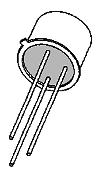
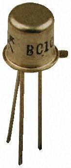
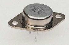
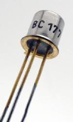
6 Characteristics (5) Depending on the constructor and application type for which transistor is made, it may present different shapes and sizes. C E B C B E
7
8 Models (1) To describe the behavior of these devices several equivalent circuits can be used, suitable for: different operating conditions (continuous, large signal and small signal) and different configurations (CB, CE and CC). Equivalent circuits can be simplified considering the desired degree of approximation. For DC (or for large lowfrequency signal by replacing h FE with b) the following model can be considered : V I V hfe h FE 0 1 CE CE B I I h I h V BE I C h FE I B V CE In this model the Early effect is considered Where I C is function of two independent variables I B and V CE. C B FE B FE 0 1 I C V CE 0 V A I C V A Taking into account that I B is a function of V BE V A V CE (dependence on V CE is neglected): I B I h S FE0 e V V BE T V I 1 CE C IS e VA V V BE T
9 Models (2) Assuming constant h FE, you get a simplification where the effect Early is neglected and characteristics (in the active region) are horizontal therefore independent from V CE. Therefore, only the independent variable I B remains. It determines the distribution of characteristics. I C V BE I B I C h FE I B I I h ; h h C B FE FE FE0 I B I h S FE e V V BE T I B V CE Further simplification, V BE is assumed constant and equal to V BEon, consequently the characteristics are uniformly distributed. This model will be used for the synthesis of the proposed stages. I C I B V BEon h FE I B h FE h FE0 I I h C B FE I B V CE
10 Models (3) For small signal the device can be described by a linear model, in which its elements have constant values depending on the bias point (V CE,V BE, I C ). The most utilized model is the Hparameter model, which is obtained through linear approximation (first order) of electric quantities which characterize its behaviour as a two port network. In particular, considering the common emitter configuration, i b and v ce are selected as independent variables and i c and v be are the dependent variables. If the condition of small variation around the quiescent point is verified. The functions i c (i b, v ce ) and v be (i b, v ce ) can be developed in the Taylor series assuming only the terms of first order : v h i h v be ie b re ce i h i h v h fe i b c fe b oe ce v be i b h ie h re v ce h oe v ce
11 Models (4) CEC h parameters I B I B DV CE V CEQ DI B DV BE h ie DV D I BE B V V CE CEQ I BQ V CE1 V CE2 DV BE h re DV D V BE CE I B I BQ V BE V BE I C DIC I B2 I B1 h fe DI B DI D I C B V CE V CEQ DI C I C I BQ I B h oe DI D V C CE I B I BQ V CEQ V CE DV CE V CE
12 Models (5) For small signal the following models are available: v be i b h ie h fe i b h oe h rev ce h parameter model v ce v be i b h ie h fe i b h oe v ce R i b v be h ie h fe i b vce Simplified model Se 1/h oe >10R C b c r bb r b c r bb BB v be v b e C b e g m v b e r b e r ce v ce v be v b e g m v b e r b e r ce v ce v b e g m v b e r b e r ce Hybridp model Simplified hybridp model h parameter model of CBC where h rb is neglected. E i e v eb h fb i e v eb h ib h o B b C E i e h ib B h fb i e C
13 Models (6) Relations between the h parameters of the CEC and the hybrid modelp parameters [1]. v ic ic h r r h r ' r ' g i v be ie bb' b' e ib v 0 ce fe b e b e m b v 0 b' e v 0 ce ce h oe i c c ce i 0 ce v 0 ce b i v v r b ' e 1 h parameters of the CBC. h ib v i eb c cb rb ' e hfb ' ob ie i ic v e ie 0 cb0 vcb0 h v r c Parameters in terms of bias current [1]. g m ic Ic 1 v V r b' e v 0 T e ce i 1 C VCE c 0 ce vce v 0 A A CEQ be ' I I CQ r v V V V r be ' V I T E [1] Electronics: a systems approach by N. Storey

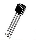
14 Datasheet (1) The BJT operation is described by a number of parameters collected and supplied by producers in datasheets. Datasheets contain several descriptive sections including: General informations: which describe the essential characteristics of the component. Pin connection: that specify the connections of the connectors Absolute maximum ratings: operating limits beyond which the IC may be damaged. Thermal data: thermal resistance. Electrical charatteristics: electrical properties of the device allow to predict the operation of the device.
15 Datasheet (2) Absolute maximum ratings Thermal data
16 Datasheet (3) Electrical charatteristics (1)
17 Datasheet (4) Sometimes a graph of V BEON values function of the current I C is given.
18 Datasheet (3) Electrical charatteristics (1)

19 Datasheet (4) Typically, for a given biasing (I C, V CE ) in the datasheet the following values of h FE may be supplied : 1. h FEmin the minimum possible value of h FE 2. h FEtyp typical value of h FE 3. h FEmax the maximum possible value of h FE During the analysis or synthesis the typical value of h FE should be used. If this value is not provided it can be estimated by the geometric mean of h FEmin and h FEmax : h h h FE FE min FE max h FE depends on the V CE (for Early effect) and by I C. The relationship between I C and h FE, in the datasheet, is described by the Normalized DC Current Gain (h FEN ) shown in the figure. h FEN hfe h ( I 2 ma) FE C h h ( I 2 ma) h FE FE C FEN

20 Datasheet (6) Sometimes a graph of the h FE values function of the current is provided.
21 Datasheet (4) Electrical charatteristics (2) If the typical values of the h parameters are not provided in the datasheet, they can be estimated by geometric mean between the minimum and maximum values. In addition, using the minimum or maximum values of the h parameters the worst or highest performance can be estimated.
22
Bipolar Junction Transistor (BJT) - Introduction
 - Introduction") Bipolar Junction Transistor (BJT) - Introduction It was found in 1948 at the Bell Telephone Laboratories. It is a three terminal device and has three semiconductor regions. It can be used in signal amplification
Bipolar Junction Transistor (BJT) - Introduction It was found in 1948 at the Bell Telephone Laboratories. It is a three terminal device and has three semiconductor regions. It can be used in signal amplification
CHAPTER.4: Transistor at low frequencies
 CHAPTER.4: Transistor at low frequencies Introduction Amplification in the AC domain BJT transistor modeling The re Transistor Model The Hybrid equivalent Model Introduction There are three models commonly
DC Biasing. Dr. U. Sezen & Dr. D. Gökçen (Hacettepe Uni.) ELE230 Electronics I 15-Mar / 59
 ELE230 Electronics I 15-Mar / 59") Contents Three States of Operation BJT DC Analysis Fixed-Bias Circuit Emitter-Stabilized Bias Circuit Voltage Divider Bias Circuit DC Bias with Voltage Feedback Various Dierent Bias Circuits pnp Transistors
Contents Three States of Operation BJT DC Analysis Fixed-Bias Circuit Emitter-Stabilized Bias Circuit Voltage Divider Bias Circuit DC Bias with Voltage Feedback Various Dierent Bias Circuits pnp Transistors
Chapter 2. - DC Biasing - BJTs
 Chapter 2. - DC Biasing - BJTs Objectives To Understand : Concept of Operating point and stability Analyzing Various biasing circuits and their comparison with respect to stability BJT A Review Invented
Electronic Circuits. Bipolar Junction Transistors. Manar Mohaisen Office: F208 Department of EECE
 Electronic Circuits Bipolar Junction Transistors Manar Mohaisen Office: F208 Email: manar.subhi@kut.ac.kr Department of EECE Review of Precedent Class Explain the Operation of the Zener Diode Explain Applications
Chapter 2 - DC Biasing - BJTs
 Objectives Chapter 2 - DC Biasing - BJTs To Understand: Concept of Operating point and stability Analyzing Various biasing circuits and their comparison with respect to stability BJT A Review Invented
KOM2751 Analog Electronics :: Dr. Muharrem Mercimek :: YTU - Control and Automation Dept. 1 4 DC BIASING BJTS (CONT D II )
") KOM2751 Analog Electronics :: Dr. Muharrem Mercimek :: YTU - Control and Automation Dept. 1 4 DC BIASING BJTS (CONT D II ) Most of the content is from the textbook: Electronic devices and circuit theory,
KOM2751 Analog Electronics :: Dr. Muharrem Mercimek :: YTU - Control and Automation Dept. 1 4 DC BIASING BJTS (CONT D II ) Most of the content is from the textbook: Electronic devices and circuit theory,
(e V BC/V T. α F I SE = α R I SC = I S (3)
") Experiment #8 BJT witching Characteristics Introduction pring 2015 Be sure to print a copy of Experiment #8 and bring it with you to lab. There will not be any experiment copies available in the lab. Also
Experiment #8 BJT witching Characteristics Introduction pring 2015 Be sure to print a copy of Experiment #8 and bring it with you to lab. There will not be any experiment copies available in the lab. Also
Device Physics: The Bipolar Transistor
 Monolithic Amplifier Circuits: Device Physics: The Bipolar Transistor Chapter 4 Jón Tómas Guðmundsson tumi@hi.is 2. Week Fall 2010 1 Introduction In analog design the transistors are not simply switches
Figure 1 Basic epitaxial planar structure of NPN. Figure 2 The 3 regions of NPN (left) and PNP (right) type of transistors
 and PNP (right) type of transistors") Figure 1 Basic epitaxial planar structure of NPN Figure 2 The 3 regions of NPN (left) and PNP (right) type of transistors Lecture Notes: 2304154 Physics and Electronics Lecture 6 (2 nd Half), Year: 2007
Figure 1 Basic epitaxial planar structure of NPN Figure 2 The 3 regions of NPN (left) and PNP (right) type of transistors Lecture Notes: 2304154 Physics and Electronics Lecture 6 (2 nd Half), Year: 2007
figure shows a pnp transistor biased to operate in the active mode
 Lecture 10b EE-215 Electronic Devices and Circuits Asst Prof Muhammad Anis Chaudhary BJT: Device Structure and Physical Operation The pnp Transistor figure shows a pnp transistor biased to operate in the
Electronic Circuits 1. Transistor Devices. Contents BJT and FET Characteristics Operations. Prof. C.K. Tse: Transistor devices
 Electronic Circuits 1 Transistor Devices Contents BJT and FET Characteristics Operations 1 What is a transistor? Three-terminal device whose voltage-current relationship is controlled by a third voltage
Prof. Paolo Colantonio a.a
 Prof. Paolo olantonio a.a. 2011 12 The D bias point is affected by thermal issue due to the active device parameter variations with temperature I 1 I I 0 I [ma] V R } I 5 } I 4 } I 3 Q 2 } I 2 Q 1 } I
University of Pittsburgh
 University of Pittsburgh Experiment #8 Lab Report The Bipolar Junction Transistor: Characteristics and Models Submission Date: 11/6/2017 Instructors: Dr. Minhee Yun John Erickson Yanhao Du Submitted By:
Biasing BJTs CHAPTER OBJECTIVES 4.1 INTRODUCTION
 4 DC Biasing BJTs CHAPTER OBJECTIVES Be able to determine the dc levels for the variety of important BJT configurations. Understand how to measure the important voltage levels of a BJT transistor configuration
Chapter 5. BJT AC Analysis
 Chapter 5. Outline: The r e transistor model CB, CE & CC AC analysis through r e model common-emitter fixed-bias voltage-divider bias emitter-bias & emitter-follower common-base configuration Transistor
Transistor Characteristics and A simple BJT Current Mirror
 Transistor Characteristics and A simple BJT Current Mirror Current-oltage (I-) Characteristics Device Under Test DUT i v T T 1 R X R X T for test Independent variable on horizontal axis Could force current
MP6901 MP6901. High Power Switching Applications. Hammer Drive, Pulse Motor Drive and Inductive Load Switching. Maximum Ratings (Ta = 25 C)
") TOSHIBA Power Transistor Module Silicon Epitaxial Type (Darlington power transistor in ) High Power Switching Applications. Hammer Drive, Pulse Motor Drive and Inductive Load Switching. Industrial Applications
TOSHIBA Power Transistor Module Silicon Epitaxial Type (Darlington power transistor in ) High Power Switching Applications. Hammer Drive, Pulse Motor Drive and Inductive Load Switching. Industrial Applications
Final Examination EE 130 December 16, 1997 Time allotted: 180 minutes
 Final Examination EE 130 December 16, 1997 Time allotted: 180 minutes Problem 1: Semiconductor Fundamentals [30 points] A uniformly doped silicon sample of length 100µm and cross-sectional area 100µm 2
UNIVERSITY OF CALIFORNIA, BERKELEY College of Engineering Department of Electrical Engineering and Computer Sciences
 UNIVERSITY OF CALIFORNIA, BERKELEY College of Engineering Department of Electrical Engineering and Computer Sciences EE 105: Microelectronic Devices and Circuits Spring 2008 MIDTERM EXAMINATION #1 Time
Chapter 13 Small-Signal Modeling and Linear Amplification
 Chapter 13 Small-Signal Modeling and Linear Amplification Microelectronic Circuit Design Richard C. Jaeger Travis N. Blalock 1/4/12 Chap 13-1 Chapter Goals Understanding of concepts related to: Transistors
General Purpose Transistors
 General Purpose Transistors NPN and PNP Silicon These transistors are designed for general purpose amplifier applications. They are housed in the SOT 33/SC which is designed for low power surface mount
Basic Electronics Prof. Dr. Chitralekha Mahanta Department of Electronics and Communication Engineering Indian Institute of Technology, Guwahati
 Basic Electronics Prof. Dr. Chitralekha Mahanta Department of Electronics and Communication Engineering Indian Institute of Technology, Guwahati Module: 2 Bipolar Junction Transistors Lecture-4 Biasing
Electronic Circuits. Transistor Bias Circuits. Manar Mohaisen Office: F208 Department of EECE
 lectronic ircuits Transistor Bias ircuits Manar Mohaisen Office: F208 mail: manar.subhi@kut.ac.kr Department of Review of the Precedent Lecture Bipolar Junction Transistor (BJT) BJT haracteristics and
Homework Assignment 08
 Homework Assignment 08 Question 1 (Short Takes) Two points each unless otherwise indicated. 1. Give one phrase/sentence that describes the primary advantage of an active load. Answer: Large effective resistance
Whereas the diode was a 1-junction device, the transistor contains two junctions. This leads to two possibilities:
 Part Recall: two types of charge carriers in semiconductors: electrons & holes two types of doped semiconductors: n-type (favor e-), p-type (favor holes) for conduction Whereas the diode was a -junction
EE105 - Fall 2006 Microelectronic Devices and Circuits
 EE105 - Fall 2006 Microelectronic Devices and Circuits Prof. Jan M. Rabaey (jan@eecs) Lecture 21: Bipolar Junction Transistor Administrative Midterm Th 6:30-8pm in Sibley Auditorium Covering everything
EE 230 Lecture 31. THE MOS TRANSISTOR Model Simplifcations THE Bipolar Junction TRANSISTOR
 EE 23 Lecture 3 THE MOS TRANSISTOR Model Simplifcations THE Bipolar Junction TRANSISTOR Quiz 3 Determine I X. Assume W=u, L=2u, V T =V, uc OX = - 4 A/V 2, λ= And the number is? 3 8 5 2? 6 4 9 7 Quiz 3
Introduction to Transistors. Semiconductors Diodes Transistors
 Introduction to Transistors Semiconductors Diodes Transistors 1 Semiconductors Typical semiconductors, like silicon and germanium, have four valence electrons which form atomic bonds with neighboring atoms
The Common-Emitter Amplifier
 c Copyright 2009. W. Marshall Leach, Jr., Professor, Georgia Institute of Technology, School of Electrical and Computer Engineering. The Common-Emitter Amplifier Basic Circuit Fig. shows the circuit diagram
Biasing the CE Amplifier
 Biasing the CE Amplifier Graphical approach: plot I C as a function of the DC base-emitter voltage (note: normally plot vs. base current, so we must return to Ebers-Moll): I C I S e V BE V th I S e V th
COMPLEMENTARY NPN/PNP TRANSISTOR
 SEMICONDUCTOR DATA SHEET COMPLEMENTARY NPN/PNP TRANSISTOR FEATURES Complementary Pair One 3904-Type NPN, One 3906-Type PNP Epitaxial Planar Die Construction Ideal for Low Power Amplification and Switching
Chapter 9 Bipolar Junction Transistor
 hapter 9 ipolar Junction Transistor hapter 9 - JT ipolar Junction Transistor JT haracteristics NPN, PNP JT D iasing ollector haracteristic and Load Line ipolar Junction Transistor (JT) JT is a three-terminal
Mod. Sim. Dyn. Sys. Amplifiers page 1
 AMPLIFIERS A circuit containing only capacitors, amplifiers (transistors) and resistors may resonate. A circuit containing only capacitors and resistors may not. Why does amplification permit resonance
55:041 Electronic Circuits The University of Iowa Fall Exam 2
 Exam 2 Name: Score /60 Question 1 One point unless indicated otherwise. 1. An engineer measures the (step response) rise time of an amplifier as t r = 0.35 μs. Estimate the 3 db bandwidth of the amplifier.
ECE-305: Spring 2018 Final Exam Review
 C-305: Spring 2018 Final xam Review Pierret, Semiconductor Device Fundamentals (SDF) Chapters 10 and 11 (pp. 371-385, 389-403) Professor Peter Bermel lectrical and Computer ngineering Purdue University,
EE 230 Lecture 33. Nonlinear Circuits and Nonlinear Devices. Diode BJT MOSFET
 EE 230 Lecture 33 Nonlinear Circuits and Nonlinear Devices Diode BJT MOSFET Review from Last Time: n-channel MOSFET Source Gate L Drain W L EFF Poly Gate oxide n-active p-sub depletion region (electrically
Bipolar junction transistors
 Bipolar junction transistors Find parameters of te BJT in CE configuration at BQ 40 µa and CBQ V. nput caracteristic B / µa 40 0 00 80 60 40 0 0 0, 0,5 0,3 0,35 0,4 BE / V Output caracteristics C / ma
ECE-342 Test 2 Solutions, Nov 4, :00-8:00pm, Closed Book (one page of notes allowed)
") ECE-342 Test 2 Solutions, Nov 4, 2008 6:00-8:00pm, Closed Book (one page of notes allowed) Please use the following physical constants in your calculations: Boltzmann s Constant: Electron Charge: Free
ECE-342 Test 2 Solutions, Nov 4, 2008 6:00-8:00pm, Closed Book (one page of notes allowed) Please use the following physical constants in your calculations: Boltzmann s Constant: Electron Charge: Free
Homework Assignment 09
 Homework Assignment 09 Question 1 (Short Takes) Two points each unless otherwise indicated. 1. What is the 3-dB bandwidth of the amplifier shown below if r π = 2.5K, r o = 100K, g m = 40 ms, and C L =
BCR191.../SEMB1 BCR191/F/L3 BCR191T/W BCR191S SEMB1. Type Marking Pin Configuration Package BCR191 BCR191F BCR191L3 2=E 2=E 2=E =C 3=C 3=C
 PNP Silicon Digital Transistor Switching circuit, inverter, interface circuit, driver circuit Built in bias resistor (R = kω, R = kω ) For 6PIN packages: two (galvanic) internal isolated transistors with
ESE319 Introduction to Microelectronics. BJT Biasing Cont.
 BJT Biasing Cont. Biasing for DC Operating Point Stability BJT Bias Using Emitter Negative Feedback Single Supply BJT Bias Scheme Constant Current BJT Bias Scheme Rule of Thumb BJT Bias Design 1 Simple
2SC5748 2SC5748. Horizontal Deflection Output for HDTV&Digital TV. Maximum Ratings (Tc 25 C) Electrical Characteristics (Tc 25 C)
 Electrical Characteristics (Tc 25 C)") TOSHIBA Transistor Silicon NPN Triple Diffused Mesa Type Horizontal Deflection Output for HDTV&Digital TV. Unit: mm High voltage: VCBO = V Low saturation voltage: VCE (sat) = V (max) High speed: tf =.
TOSHIBA Transistor Silicon NPN Triple Diffused Mesa Type Horizontal Deflection Output for HDTV&Digital TV. Unit: mm High voltage: VCBO = V Low saturation voltage: VCE (sat) = V (max) High speed: tf =.
1. (50 points, BJT curves & equivalent) For the 2N3904 =(npn) and the 2N3906 =(pnp)
 For the 2N3904 =(npn) and the 2N3906 =(pnp)") HW 3 1. (50 points, BJT curves & equivalent) For the 2N3904 =(npn) and the 2N3906 =(pnp) a) Obtain in Spice the transistor curves given on the course web page except do in separate plots, one for the npn
HW 3 1. (50 points, BJT curves & equivalent) For the 2N3904 =(npn) and the 2N3906 =(pnp) a) Obtain in Spice the transistor curves given on the course web page except do in separate plots, one for the npn
Mod. Sim. Dyn. Sys. Amplifiers page 1
 AMPLIFIERS A circuit containing only capacitors, amplifiers (transistors) and resistors may resonate. A circuit containing only capacitors and resistors may not. Why does amplification permit resonance
Semiconductor Physics fall 2012 problems
 Semiconductor Physics fall 2012 problems 1. An n-type sample of silicon has a uniform density N D = 10 16 atoms cm -3 of arsenic, and a p-type silicon sample has N A = 10 15 atoms cm -3 of boron. For each
6.012 Electronic Devices and Circuits
 Page 1 of 12 YOUR NAME Department of Electrical Engineering and Computer Science Massachusetts Institute of Technology 6.012 Electronic Devices and Circuits FINAL EXAMINATION Open book. Notes: 1. Unless
SOME USEFUL NETWORK THEOREMS
 APPENDIX D SOME USEFUL NETWORK THEOREMS Introduction In this appendix we review three network theorems that are useful in simplifying the analysis of electronic circuits: Thévenin s theorem Norton s theorem
2SC4203 2SC4203. Video Output for High Definition VDT High Speed Switching Applications. Maximum Ratings (Ta = 25 C)
") TOSHIBA Transistor Silicon Epitaxial Planar Type 2SC42 Video Output for High Definition VDT High Speed Switching Applications Unit: mm High transition frequency: ft = 4 MHz (typ.) (VCE = V, IC = 7 ma)
TOSHIBA Transistor Silicon Epitaxial Planar Type 2SC42 Video Output for High Definition VDT High Speed Switching Applications Unit: mm High transition frequency: ft = 4 MHz (typ.) (VCE = V, IC = 7 ma)
Lecture 35 - Bipolar Junction Transistor (cont.) November 27, Current-voltage characteristics of ideal BJT (cont.)
 November 27, Current-voltage characteristics of ideal BJT (cont.)") 6.720J/3.43J - Integrated Microelectronic Devices - Fall 2002 Lecture 35-1 Lecture 35 - Bipolar Junction Transistor (cont.) November 27, 2002 Contents: 1. Current-voltage characteristics of ideal BJT (cont.)
6.720J/3.43J - Integrated Microelectronic Devices - Fall 2002 Lecture 35-1 Lecture 35 - Bipolar Junction Transistor (cont.) November 27, 2002 Contents: 1. Current-voltage characteristics of ideal BJT (cont.)
2SC3074 2SC3074. High Current Switching Applications. Maximum Ratings (Ta = 25 C)
") SC7 TOSHIBA Transistor Silicon NPN Epitaxial Type (PCT process) SC7 High Current Switching Applications Unit: mm Low collector saturation voltage: VCE (sat) =. V (max) (IC = A) High speed switching time:
SC7 TOSHIBA Transistor Silicon NPN Epitaxial Type (PCT process) SC7 High Current Switching Applications Unit: mm Low collector saturation voltage: VCE (sat) =. V (max) (IC = A) High speed switching time:
Silicon Diffused Power Transistor
 GENERAL DESCRIPTION High voltage, high-speed switching npn transistors in a fully isolated SOT99 envelope, primarily for use in horizontal deflection circuits of colour television receivers. QUICK REFERENCE
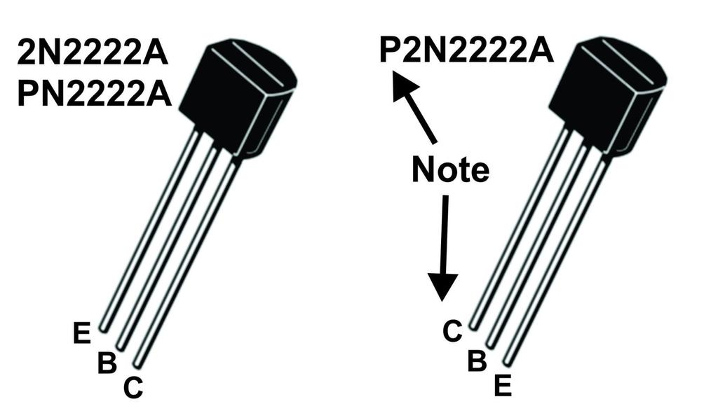
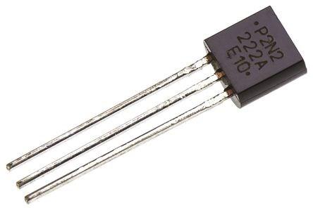
PN2222, PN2222A. General Purpose Transistors. NPN Silicon. Pb Free Packages are Available* Features MAXIMUM RATINGS MARKING DIAGRAM
 , is a Preferred Device General Purpose Transistors NPN Silicon Features PbFree Packages are Available* COLLECTOR 3 MAXIMUM RATINGS Collector-Emitter Voltage Collector-Base Voltage Rating Symbol Value
DATA SHEET. BC556; BC557 PNP general purpose transistors DISCRETE SEMICONDUCTORS. Product specification Supersedes data of 1997 Mar 27.
 DISCRETE SEMICONDUCTORS DATA SHEET book, halfpage M3D186 Supersedes data of 1997 Mar 27 FEATURES Low current (max. 100 ma) Low voltage (max. 65 V). APPLICATIONS General purpose switching and amplification.
7. DESIGN OF AC-COUPLED BJT AMPLIFIERS FOR MAXIMUM UNDISTORTED VOLTAGE SWING
 à 7. DESIGN OF AC-COUPLED BJT AMPLIFIERS FOR MAXIMUM UNDISTORTED VOLTAGE SWING Figure. AC coupled common emitter amplifier circuit ü The DC Load Line V CC = I CQ + V CEQ + R E I EQ I EQ = I CQ + I BQ I
Vidyalankar S.E. Sem. III [EXTC] Analog Electronics - I Prelim Question Paper Solution
![Vidyalankar S.E. Sem. III [EXTC] Analog Electronics - I Prelim Question Paper Solution](/thumbs/90/101612294.jpg "Vidyalankar S.E. Sem. III [EXTC] Analog Electronics - I Prelim Question Paper Solution") . (a) S.E. Sem. [EXTC] Analog Electronics - Prelim Question Paper Solution Comparison between BJT and JFET BJT JFET ) BJT is a bipolar device, both majority JFET is an unipolar device, electron and minority
. (a) S.E. Sem. [EXTC] Analog Electronics - Prelim Question Paper Solution Comparison between BJT and JFET BJT JFET ) BJT is a bipolar device, both majority JFET is an unipolar device, electron and minority
EE 330 Lecture 22. Small Signal Modelling Operating Points for Amplifier Applications Amplification with Transistor Circuits
 EE 330 Lecture 22 Small Signal Modelling Operating Points for Amplifier Applications Amplification with Transistor Circuits Exam 2 Friday March 9 Exam 3 Friday April 13 Review Session for Exam 2: 6:00
BJT Biasing Cont. & Small Signal Model
 BJT Biasing Cont. & Small Signal Model Conservative Bias Design (1/3, 1/3, 1/3 Rule) Bias Design Example Small-Signal BJT Models Small-Signal Analysis 1 Emitter Feedback Bias Design R B R C V CC R 1 R
Engineering 1620 Spring 2011 Answers to Homework # 4 Biasing and Small Signal Properties
 Engineering 60 Spring 0 Answers to Homework # 4 Biasing and Small Signal Properties.).) The in-band Thevenin equivalent source impedance is the parallel combination of R, R, and R3. ( In-band implies the
BJT Biasing Cont. & Small Signal Model
 BJT Biasing Cont. & Small Signal Model Conservative Bias Design Bias Design Example Small Signal BJT Models Small Signal Analysis 1 Emitter Feedback Bias Design Voltage bias circuit Single power supply
Digital Integrated CircuitDesign
 Digital Integrated CircuitDesign Lecture 5a Bipolar Transistor Dep. Region Neutral Base n(0) b B C n b0 P C0 P e0 P C xn 0 xp 0 x n(w) b W B Adib Abrishamifar EE Department IUST Contents Bipolar Transistor
ELEC 3908, Physical Electronics, Lecture 17. Bipolar Transistor Injection Models
 LC 3908, Physical lectronics, Lecture 17 Bipolar Transistor njection Models Lecture Outline Last lecture looked at qualitative operation of the BJT, now want to develop a quantitative model to predict
Lecture 17. The Bipolar Junction Transistor (II) Regimes of Operation. Outline
 Regimes of Operation. Outline") Lecture 17 The Bipolar Junction Transistor (II) Regimes of Operation Outline Regimes of operation Large-signal equivalent circuit model Output characteristics Reading Assignment: Howe and Sodini; Chapter
Lecture 17 The Bipolar Junction Transistor (II) Regimes of Operation Outline Regimes of operation Large-signal equivalent circuit model Output characteristics Reading Assignment: Howe and Sodini; Chapter
Circle the one best answer for each question. Five points per question.
 ID # NAME EE-255 EXAM 3 November 8, 2001 Instructor (circle one) Talavage Gray This exam consists of 16 multiple choice questions and one workout problem. Record all answers to the multiple choice questions
Capacitors Diodes Transistors. PC200 Lectures. Terry Sturtevant. Wilfrid Laurier University. June 4, 2009
 Wilfrid Laurier University June 4, 2009 Capacitor an electronic device which consists of two conductive plates separated by an insulator Capacitor an electronic device which consists of two conductive
FYSE400 ANALOG ELECTRONICS
 YSE400 ANALOG ELECTONCS LECTUE 3 Bipolar Sub Circuits 1 BPOLA SUB CCUTS Bipolar Current Sinks and -Sources Transistor operates in forwardactive region. < < sat CE CN max CE < < + BN CN BN max CE N N N
2N4918-2N4920 Series. Medium-Power Plastic PNP Silicon Transistors 3.0 A, V, 30 W GENERAL PURPOSE POWER TRANSISTORS
 2N4918-2N492 Series Medium-Power Plastic PNP Silicon Transistors These mediumpower, highperformance plastic devices are designed for driver circuits, switching, and amplifier applications. Features Low
Introduction to Power Semiconductor Devices
 ECE442 Power Semiconductor Devices and Integrated Circuits Introduction to Power Semiconductor Devices Zheng Yang (ERF 3017, email: yangzhen@uic.edu) Power Semiconductor Devices Applications System Ratings
2SC3457. isc Silicon NPN Power Transistor. isc Product Specification. INCHANGE Semiconductor. isc Website:
 INCHANGE Semiconductor isc Silicon NPN Power Transistor isc Product Specification DESCRIPTION High Breakdown oltage- : (BR)CBO = 1100(Min) Fast Switching Speed Wide Area of Safe Operation APPLICATIONS
ELEC 3908, Physical Electronics, Lecture 19. BJT Base Resistance and Small Signal Modelling
 ELEC 3908, Physical Electronics, Lecture 19 BJT Base Resistance and Small Signal Modelling Lecture Outline Lecture 17 derived static (dc) injection model to predict dc currents from terminal voltages This
DISCRETE SEMICONDUCTORS DATA SHEET. BFQ19 NPN 5 GHz wideband transistor. Product specification File under Discrete Semiconductors, SC14
 DISCRETE SEMICONDUCTORS DATA SHEET File under Discrete Semiconductors, SC14 September 1995 DESCRIPTION PINNING NPN transistor in a SOT89 plastic envelope intended for application in thick and thin-film
Silicon Diffused Power Transistor
 PHE139 GENERAL DESCRIPTION The PHE139 is a silicon npn power switching transistor in the TO22AB envelope intended for use in high frequency electronic lighting ballast applications, converters, inverters,
2N4921, 2N4922, 2N4923. Medium Power Plastic NPN Silicon Transistors 1.0 AMPERE GENERAL PURPOSE POWER TRANSISTORS VOLTS, 30 WATTS
 2N4923 is a Preferred Device MediumPower Plastic NPN Silicon Transistors These highperformance plastic devices are designed for driver circuits, switching, and amplifier applications. Features Low Saturation
Small-Signal Midfrequency BJT Amplifiers
 Small-Signal Midfrequency JT Amplifiers 6.. INTRODUTION For sufficiently small emitter-collector voltage and current excursions about the quiescent point (small signals), the JT is considered linear; it
ACADAMIC CHAPTER OF SWECHA September- 2010
 Swecha Documents SF-SAC/ ECE / II-II/LM/2010 /ver. 1.0 LABMANAUALS DEPARTMENT : ECE ELECTRONIC CIRCUITS ANALYSIS LABORATORY MANUAL ACADAMIC CHAPTER OF SWECHA September- 2010 INDEX S.NO NAME OF THE EXPERIMENT
absolute maximum ratings at 25 C case temperature (unless otherwise noted)
") ,, B, C, D Designed for Complementary Use with BDW84, BDW84A, BDW84B, BDW84C and BDW84D W at C Case Temperature A Continuous Collector Current Minimum h FE of 70 at 3, 6 A B C E SOT-93 PACKAGE (TOP IEW)
,, B, C, D Designed for Complementary Use with BDW84, BDW84A, BDW84B, BDW84C and BDW84D W at C Case Temperature A Continuous Collector Current Minimum h FE of 70 at 3, 6 A B C E SOT-93 PACKAGE (TOP IEW)
Bipolar junction transistor operation and modeling
 6.01 - Electronic Devices and Circuits Lecture 8 - Bipolar Junction Transistor Basics - Outline Announcements Handout - Lecture Outline and Summary; Old eam 1's on Stellar First Hour Eam - Oct. 8, 7:30-9:30
BC487, BC487B. High Current Transistors. NPN Silicon. Pb Free Packages are Available* Features. MAXIMUM RATINGS MARKING DIAGRAM
 High Current Transistors NPN Silicon Features PbFree Packages are Available* COLLECTOR 1 MAXIMUM RATINGS Rating Symbol alue Unit Collector Emitter oltage CEO 60 dc Collector Base oltage CBO 60 dc Emitter
KSD1621 NPN Epitaxial Silicon Transistor
 KSD62 NPN Epitaxial Silicon Transistor High Current Driver Applications Low Collector-Emitter Saturation Voltage Large Current Capacity and Wide SOA Fast Switching Speed Complement to KSB2 Marking 6 2
Chapter 3 Output stages
 Chapter 3 utput stages 3.. Goals and properties 3.. Goals and properties deliver power into the load with good efficacy and small power dissipate on the final transistors small output impedance maximum
Silicon Diffused Darlington Power Transistor
 GENERAL DESCRIPTION Highvoltage, monolithic npn power Darlington transistor in a SOT93 envelope intended for use in car ignition systems, DC and AC motor controls, solenoid drivers, etc. QUICK REFERENCE
0.016 W/ C to +150 C
 MJF00 (NPN), MJF0 (PNP) Complementary Power Transistors For Isolated Package Applications Designed for general purpose amplifier and switching applications, where the mounting surface of the device is
Experiment Determining the beta where it is stable.(6) Analysis and design of dc-biased transistor configurations (9)
 Analysis and design of dc-biased transistor configurations (9)") Visit http://electronicsclub.cjb.net for more resources DC BIASING BJTs (Analysis & Design) Design Procedure..(3) Limits of operation....(3) BJT modes of operation...(4) The Beta(h FE ).....(5) Experiment
Visit http://electronicsclub.cjb.net for more resources DC BIASING BJTs (Analysis & Design) Design Procedure..(3) Limits of operation....(3) BJT modes of operation...(4) The Beta(h FE ).....(5) Experiment
Semiconductor Physics Problems 2015
 Semiconductor Physics Problems 2015 Page and figure numbers refer to Semiconductor Devices Physics and Technology, 3rd edition, by SM Sze and M-K Lee 1. The purest semiconductor crystals it is possible
The Devices. Jan M. Rabaey
 The Devices Jan M. Rabaey Goal of this chapter Present intuitive understanding of device operation Introduction of basic device equations Introduction of models for manual analysis Introduction of models
13. Bipolar transistors
 Technische Universität Graz Institute of Solid State Physics 13. Bipolar transistors Jan. 16, 2019 Technische Universität Graz Institute of Solid State Physics bipolar transistors npn transistor collector
BC556B, BC557A, B, C, BC558B. Amplifier Transistors. PNP Silicon BC556B PNP AUDIO 100MA 65V 500MW TO92.
 B, A, B, C, B Amplifier Transistors PNP Silicon Features PbFree Packages are Available* B PNP AUDIO 1MA 65 5MW TO92 COLLECTOR 1 MAXIMUM RATINGS Collector - Emitter oltage Collector - Base oltage Rating
Tutorial #4: Bias Point Analysis in Multisim
 SCHOOL OF ENGINEERING AND APPLIED SCIENCE DEPARTMENT OF ELECTRICAL AND COMPUTER ENGINEERING ECE 2115: ENGINEERING ELECTRONICS LABORATORY Tutorial #4: Bias Point Analysis in Multisim INTRODUCTION When BJTs
assess the biasing requirements for transistor amplifiers
 1 INTODUTION In this lesson we examine the properties of the bipolar junction transistor (JT) amd its typical practical characteristics. We then go on to devise circuits in which we can take best advantage
Chapter 1 Introduction to Electronics
 Chapter Introduction to Electronics Section - Atomic Structure. An atom with an atomic number of 6 has 6 electrons and 6 protons.. The third shell of an atom can have n = (3) = 8 electrons. Section - Materials
Class AB Output Stage
 Class AB Output Stage Class AB amplifier Operation Multisim Simulation - VTC Class AB amplifier biasing Widlar current source Multisim Simulation - Biasing 1 Class AB Operation v I V B (set by V B ) Basic
Memories Bipolar Transistors
 Technische Universität Graz nstitute of Solid State Physics Memories Bipolar Transistors Technische Universität Graz nstitute of Solid State Physics Exams February 5 March 7 April 18 June 27 Exam Four
Lecture 7: Transistors and Amplifiers
 Lecture 7: Transistors and Amplifiers Hybrid Transistor Model for small AC : The previous model for a transistor used one parameter (β, the current gain) to describe the transistor. doesn't explain many
DATA SHEET. BC368 NPN medium power transistor; 20 V, 1 A DISCRETE SEMICONDUCTORS. Product specification Supersedes data of 2003 Dec 01.
 DISCRETE SEMICONDUCTORS DATA SHEET book, halfpage M3D86 Supersedes data of 2003 Dec 0 2004 Nov 05 FEATURES High current. APPLICATIONS Linear voltage regulators Low side switch Supply line switch for negative
Electronic Circuits Summary
 Electronic Circuits Summary Andreas Biri, D-ITET 6.06.4 Constants (@300K) ε 0 = 8.854 0 F m m 0 = 9. 0 3 kg k =.38 0 3 J K = 8.67 0 5 ev/k kt q = 0.059 V, q kt = 38.6, kt = 5.9 mev V Small Signal Equivalent
DISCRETE SEMICONDUCTORS DATA SHEET. BFQ149 PNP 5 GHz wideband transistor. Product specification File under Discrete Semiconductors, SC14
 DISCRETE SEMICONDUCTORS DATA SHEET File under Discrete Semiconductors, SC14 September 1995 DESCRIPTION PINNING PNP transistor in a SOT89 envelope. It is intended for use in UHF applications such as broadband
EC/EE DIGITAL ELECTRONICS
 EC/EE 214(R-15) Total No. of Questions :09] [Total No. of Pages : 02 II/IV B.Tech. DEGREE EXAMINATIONS, DECEMBER- 2016 First Semester EC/EE DIGITAL ELECTRONICS Time: Three Hours 1. a) Define Encoder Answer
ID # NAME. EE-255 EXAM 3 April 7, Instructor (circle one) Ogborn Lundstrom
 Ogborn Lundstrom") ID # NAME EE-255 EXAM 3 April 7, 1998 Instructor (circle one) Ogborn Lundstrom This exam consists of 20 multiple choice questions. Record all answers on this page, but you must turn in the entire exam.
ID # NAME EE-255 EXAM 3 April 7, 1998 Instructor (circle one) Ogborn Lundstrom This exam consists of 20 multiple choice questions. Record all answers on this page, but you must turn in the entire exam.
EE 330 Lecture 25. Amplifier Biasing (precursor) Two-Port Amplifier Model
 Two-Port Amplifier Model") EE 330 Lecture 25 Amplifier Biasing (precursor) Two-Port Amplifier Model Review from Last Lecture Exam Schedule Exam 2 Friday March 24 Review from Last Lecture Graphical Analysis and Interpretation 2 OX
EE 330 Lecture 25 Amplifier Biasing (precursor) Two-Port Amplifier Model Review from Last Lecture Exam Schedule Exam 2 Friday March 24 Review from Last Lecture Graphical Analysis and Interpretation 2 OX